EP0012065B1 - Détecteur de radiation d'un appareil de tomographie - Google Patents
Détecteur de radiation d'un appareil de tomographie Download PDFInfo
- Publication number
- EP0012065B1 EP0012065B1 EP79400892A EP79400892A EP0012065B1 EP 0012065 B1 EP0012065 B1 EP 0012065B1 EP 79400892 A EP79400892 A EP 79400892A EP 79400892 A EP79400892 A EP 79400892A EP 0012065 B1 EP0012065 B1 EP 0012065B1
- Authority
- EP
- European Patent Office
- Prior art keywords
- conductors
- chamber
- cover
- radiation detector
- conductive layers
- Prior art date
- Legal status (The legal status is an assumption and is not a legal conclusion. Google has not performed a legal analysis and makes no representation as to the accuracy of the status listed.)
- Expired
Links
- 230000005855 radiation Effects 0.000 title claims description 16
- 239000004020 conductor Substances 0.000 claims description 52
- 238000003325 tomography Methods 0.000 claims description 34
- 238000005259 measurement Methods 0.000 claims description 29
- 238000001514 detection method Methods 0.000 claims description 19
- 230000010287 polarization Effects 0.000 claims description 10
- 239000011810 insulating material Substances 0.000 claims description 5
- 238000007789 sealing Methods 0.000 claims description 3
- 238000005513 bias potential Methods 0.000 description 8
- 210000000056 organ Anatomy 0.000 description 6
- 239000011324 bead Substances 0.000 description 4
- RYGMFSIKBFXOCR-UHFFFAOYSA-N Copper Chemical compound [Cu] RYGMFSIKBFXOCR-UHFFFAOYSA-N 0.000 description 3
- 229910052802 copper Inorganic materials 0.000 description 3
- 239000010949 copper Substances 0.000 description 3
- 229920000297 Rayon Polymers 0.000 description 2
- 239000003990 capacitor Substances 0.000 description 2
- 239000012212 insulator Substances 0.000 description 2
- 239000002964 rayon Substances 0.000 description 2
- 238000012800 visualization Methods 0.000 description 2
- 239000004593 Epoxy Substances 0.000 description 1
- 239000004952 Polyamide Substances 0.000 description 1
- 239000004809 Teflon Substances 0.000 description 1
- 229920006362 Teflon® Polymers 0.000 description 1
- 238000010586 diagram Methods 0.000 description 1
- 238000005530 etching Methods 0.000 description 1
- 239000011152 fibreglass Substances 0.000 description 1
- 239000011521 glass Substances 0.000 description 1
- 238000009413 insulation Methods 0.000 description 1
- 229920003223 poly(pyromellitimide-1,4-diphenyl ether) Polymers 0.000 description 1
- 229920002647 polyamide Polymers 0.000 description 1
- -1 polytetrafluoroethylene Polymers 0.000 description 1
- 229920001343 polytetrafluoroethylene Polymers 0.000 description 1
- 239000004810 polytetrafluoroethylene Substances 0.000 description 1
- 229910052724 xenon Inorganic materials 0.000 description 1
- FHNFHKCVQCLJFQ-UHFFFAOYSA-N xenon atom Chemical compound [Xe] FHNFHKCVQCLJFQ-UHFFFAOYSA-N 0.000 description 1
Images


Classifications
-
- H—ELECTRICITY
- H01—ELECTRIC ELEMENTS
- H01J—ELECTRIC DISCHARGE TUBES OR DISCHARGE LAMPS
- H01J47/00—Tubes for determining the presence, intensity, density or energy of radiation or particles
- H01J47/02—Ionisation chambers
-
- H—ELECTRICITY
- H01—ELECTRIC ELEMENTS
- H01J—ELECTRIC DISCHARGE TUBES OR DISCHARGE LAMPS
- H01J5/00—Details relating to vessels or to leading-in conductors common to two or more basic types of discharge tubes or lamps
- H01J5/32—Seals for leading-in conductors
- H01J5/44—Annular seals disposed between the ends of the vessel
Definitions
- the present invention relates to a radiation detector of a tomography device which comprises in particular an enclosure closed by a cover, detection electrodes in this enclosure and means of interconnection between these electrodes and conductive terminals external to the enclosure.
- This detector applies more particularly to a tomography device in which it is necessary to provide a large number of connectors between electrodes contained in an enclosure closed by a cover and conductive terminals external to this enclosure and in which it is necessary to '' avoid leakage currents between these connectors and the conductive parts of the enclosure and cover.
- an X-ray tomography device comprises a detector constituted by detection cells delimited by measurement electrodes brought to a polarization potential and housed in a housing one face of which receives X-rays and the bottom of which is closed by a cover.
- this box is filled with pressurized gas, such as xenon for example.
- pressurized gas such as xenon for example.
- the detection cells In order to be able to obtain an image of an organ observed using the apparatus, it is necessary to connect the detection cells to electronic channels for measuring the currents received by each electrode. In order to improve the spatial resolution of the device, it is necessary that the number of detection cells is very large. Currently, this number can reach 500 and even 1000 detection cells.
- the number of electrodes is of course also large and in a device having 500 to 1000 detection cells, 500 to 1000 connections are necessary to connect the tomography device to the different measurement channels. Generally, these connections are made by wire-to-wire wiring, at the outlet of the housing, and, in order to isolate the various wires of the wiring and the housing, these wires exit from the housing through beads soldered or glued to this housing.
- the large number of electrodes required by the increase in spatial resolution makes it difficult, even impossible, the mechanical arrangement of 500 to 1000 glass beads.
- An exemplary embodiment of a tomography device having a very large number of cells is given in European patent application EP-A-10,474 with French priority of October 13, 1978 in the name of the same applicant.
- the flexible flat cable consists of conductors embedded in an insulating sheet inserted between two conductive layers themselves inserted between two insulating layers.
- the detector described in this patent does not make it possible, due to the connection means which it uses, to avoid the leakage currents which appear when passing through the enclosure. It also does not make it possible to connect a large number of electrodes contained in the enclosure, with a large number of conductive terminals outside this enclosure, due to the presence of bulky insulating crosspieces.
- connection means which could possibly make it possible to connect a large number of internal electrodes to an enclosure of a tomography apparatus, with a large number of conductive terminals external to the enclosure, is described in patent FR-A-1 399,458.
- This patent describes an interconnection device by conductors between conductive terminals inside an enclosure closed by a removable cover and conductive terminals outside this enclosure, in which the conductors pass between the enclosure and the cover, these conductors being embedded in a sheet of insulating material which electrically insulates them from each other and from the enclosure and its cover.
- This device makes it possible to connect a large number of internal conductive terminals to an enclosure with a large number of external terminals to this enclosure.
- it is not intended to solve a problem of leakage currents when crossing the enclosure.
- the object of the invention is to remedy the drawbacks of the radiation detector described above and in particular to produce a radiation detector for a tomography device in which it is necessary to provide a large number of conductors between electrodes contained in a closed enclosure. by a cover and conductive terminals outside this enclosure, while avoiding leakage currents between these conductors and the conductive parts of the enclosure and of the cover.
- These aims are achieved by embedding the conductors in an insulating sheet surrounded by conductive layers brought to the same potential as that to which the conductors are borne. These conductive layers are themselves embedded in insulating layers.
- the detector of the invention also makes it possible to avoid the use of insulating beads between the enclosure and its cover.
- the subject of the invention is a radiation detector of a tomography device, comprising an enclosure closed by a removable cover, a plurality of detection electrodes disposed in said closed enclosure, capable of presenting variable potentials to be measured, and means for interconnecting by conductors said internal detection electrodes to said enclosure and conductive terminals outside this enclosure, characterized in that said interconnection means have the form of a ribbon passing between the enclosure and the cover, said tape comprising said conductors embedded in a sheet of insulating material which electrically insulates them from each other and with respect to the enclosure and its cover, said sheet of insulating material being inserted between two conductive layers, themselves inserted between two insulating layers located respectively facing the enclosure and the cover, said electrodes being intended to be worn by means of said conductors at a determined polarization potential, and said conductive layers being intended to be brought to the same polarization potential as said conductors, in order to avoid the appearance of leakage currents in the insulator surrounding these conductors.
- said insulating sheet covers the periphery of the interface between the enclosure and the cover.
- two sealing O-rings are respectively arranged opposite one and the other faces of said insulating sheet.
- the conductors are subdivided into a first and a second group each inserted separately between two conductive layers, the conductors of said first and second groups being intended to be brought respectively to a first and to a second bias potential and said layers conductors being intended to be brought respectively to the same polarization potential as that of the corresponding group of conductors.
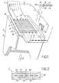
- a radiation detector of a tomography device provided with an interconnection device 1 according to the invention.
- This device allows the interconnection of the detection cells 2 of an X-ray tomography apparatus 3, with measurement channels not shown in this figure. These channels make it possible to view the image of an organ, on the basis of signals received from the detection cells, when the latter are subjected to X-ray radiation represented at R and having passed through the organ to be radiographed.
- the detection cells of the tomography device 3 are housed in a housing 4, one side of which, not shown, receives X-rays and the bottom 5 of which is closed by a cover 6.
- the interconnection device 1 has the form of a ribbon which passes through the housing at the interface 8 which separates the housing from its cover.
- This device 'interconnection comprises conductors 9 which will be described later in detail; -these conductors 9 are isolated from each other and are insulated from the housing, in particular by an insulating sheet 10 in which they may be embedded; this insulating sheet 10 is covered on each of its faces respectively by conductive layers 11, 12, themselves covered with insulating layers 13, 14.
- these conductive layers are brought to the polarization potential of the electrodes, in order to avoid the appearance of leakage currents in the insulation surrounding these conductors.
- These conductive layers act in the same way as a guard ring surrounding a threadlike conductor which would be brought to the same potential as this conductor.
- the interconnection device 1 can have the form shown in the figure, so as to cooperate with O-rings 15, 16 intended to ensure a perfect seal between the cover and the housing. It is obvious that the lateral portions 33 of the interconnection device only comprise, at the level of the housing, the insulating layers and plies and, possibly, only the conductive layers.
- the conductors are connected to the electrodes 7 in the manner shown at 32.
- this device comprises conductors 9 which are isolated from each other and which are isolated from the housing of the tomography apparatus, by virtue of a structure which comprises an insulating sheet 10 containing these conductors; this insulating sheet is covered on each of its faces respectively, by conductive layers 11, 12 themselves covered with insulating layers 13, 14.
- the conductors 9 are preferably parallel tapes made of copper by etching a continuous layer by example; the conductive layers 11, 12 can also be copper layers deposited on the faces of the sheet 10.
- This sheet 10 can consist of two layers 18, 19; layer 18, for example, initially carries the copper layer in which the conductive strips 9 are etched, which join each electrode to each electronic channel.
- the conductive layers 11, 12 are brought to the same polarization potential as that of the electrodes to which the conductors 9 are connected. These conductive layers 11, 12 act as guard rings between the conductive strips and the conductive mass of the housing of the tomography device.
- the insulating layers can be made of polytetrafluoroethylene, better known under the trade name of teflon, polyamide (“Kapton”) or epoxy reinforced with fiberglass.
- Fig. 3 provides a better understanding of the interconnection of the device according to the invention, between the detection cells 2 of an X-ray tomography device 3 and the measurement channels 20 and 27 of an electronic assembly 21 allowing a visualization of the organ radiographed by the tomography apparatus 3.
- This device can be of the same type as that described in the aforementioned patent application. It is assumed in this figure that the tomography apparatus is seen on its rear face and that the radiation R is perpendicular to the plane of the figure.
- This tomography device is of the multicellular type and the detection cells include a plurality of anodes 7 and cathodes 22 arranged alternately on insulating bars represented schematically at 23 and 24.
- the bars and the electrodes are arranged in the box 4, closed by the cover 6 held by screws 30.
- the sealing is ensured by means of the O-rings 15, 16 mentioned above. In this figure, only the seal 15 is visible.
- the insulating bars can be covered on their face opposite the ends of the electrodes which they support, with a conductive layer. These bars will be better described later.
- the electrodes 7 are for example brought to a positive bias potential with respect to a reference potential M, by virtue of an electrical supply 25, and constitute anodes.
- the electrodes such as 22 are brought to a negative bias potential with respect to a reference potential M, thanks to a power supply 26, and constitute cathodes.
- the measurement channels 27 are connected to the anodes 7 by the conductors 9 of the interconnection device 1 according to the invention.
- the interconnection device comprises, for the upper part of the device shown, conductors 9 embedded for example in the insulating layer 19 and covered by the insulating layer 18.
- the layers are also distinguished in the figure. conductors 11 and 12, themselves covered with insulating layers 13, 14.
- the conductive layers 11, 12 are carried by the conductor 42 at the same predetermined positive potential as that of the anodes 7, thanks to the power supply 25.
- the power supply 25 also allows on the one hand to apply this bias potential to the anodes 7 via the measurement channels 27, the circuit 32 and the conductors 9, and on the other hand to apply this potential to the conductive layer which covers the bars 23, which support the electrodes, as will be seen below in detail.
- the conductive layers 11 and 12 of the interconnection device which are continuous and brought to the same potential as the corresponding electrodes, act as a guard ring between the conductors 9 and the reference potential M to which the housing 4 of the tomography device 3.
- the interconnection device 1 makes it possible to connect the cathodes 22 to the measurement channels 20 of the electronic assembly 21, by means of the conductors 28, similar to the conductors 9 via the circuit 33.
- the negative potential of the power supply 26 is applied to the two conductive layers 11, 12 by the circuit 31.
- This negative bias potential is also applied via the measurement channels 20, of the circuit 33 and conductors 28 at each of the cathodes 22, as well as at the conductive layer covering the strip 24 which supports these cathodes, as will be seen below in detail.
- the conductive layers 11 and 12 follow the contour of the bottom of the housing 4, but they are of course interrupted in the middle part 40, 41 of this contour. Indeed, these conductive layers are brought to a positive potential in the upper part of the device (namely left part in the drawing) and to a negative potential in the lower part (right part in the drawing), for example.
- the insulating layers 13, 14, 18 and 19 are however continuous over the entire contour of the bottom of the housing 4.
- the bias potential of the anodes 7 is applied to these anodes by the circuit 32, which also serves to collect the measurement signals to be applied to the channels 27 of the electronic display assembly 21.
- the power supply 25 is connected to the positive inputs of the operational amplifiers 34, the negative inputs of which are connected to the circuit 32.
- the negative input of each operational amplifier is connected to the output of this amplifier via a feedback circuit 35 which can, for example, be a capacitor. These are the outputs 36 of these operational amplifiers which are connected to the display unit 5 of the assembly 21.
- the cathodes 22 are connected to the power supply 26 via the operational amplifiers 37.
- the negative input of each of these amplifiers is also connected to its output via a capacitor 38, by example.
- the outputs 39 of the amplifiers 37 are connected to the display unit 5.
- the overall resolution of the tomography device is double the resolution obtained in the case where only the cathodes are joined to the measurement channels. It is therefore possible, thanks to the interconnection device according to the invention, to use a tomography device which can have two parts; one of these parts can be intended for the visualization of an organ with a high spatial resolution and in this case, the anodes and the cathodes of this part are connected to the measurement channels; the other part can be intended for the display of an organ not requiring a high spatial resolution, in this case, only the cathodes are connected to the measurement channels of the electronic display assembly.
- FIG. 4 With reference to fig. 4, there is shown the tomography apparatus of FIG. 3, in section along a plane IV-IV perpendicular to the plane of FIG. 3. Only the upper part of the tomography apparatus (namely the right side part in the drawing) has been shown in this figure.
- the connection device according to the invention is shown at 1 in this figure.
- the conductors 9 are connected to the anodes 7, but it is obvious that in the lower part of the tomography apparatus, identical conductors 28 are connected to the cathodes.
- These conductors are, moreover, connected by connections 32 to the power supply 25, by means of operational amplifiers described above.
- This supply is that which allows the anodes to be brought to a positive bias voltage.
- the conductors 9 are embedded in the insulating layers 18, 19, themselves covered with the conductive layers 11, 12 connected at 42 to the power supply 25. These conductive layers are themselves covered by the insulating layers 13, 14.
- the layer conductive 12, as indicated above as well as in the aforementioned patent application, is connected at 43 to the conductive layers 45, 46, which cover the insulating bars supporting the anodes 7 which form a guard ring, at the base of these insulating bars .
- An electrical connection 47 makes it possible to bring the conductive layers covering the insulating bars supporting the anodes to the positive high voltage, at the bottom not shown of the tomography apparatus.
- connection device located at the lower part (not shown) of the tomography apparatus makes it possible to bring the cathodes 22 to a negative bias voltage and to apply this voltage via the electrical connection 48, to the conductive layers 49, 50 which cover the base of the bars supporting the cathodes.
- the interconnection device which has just been described has been assumed to be applied to the interconnection of the detection cells and of the measurement channels in an X-ray tomography apparatus in which all the electrodes are measurement electrodes. Therefore, the interconnection device has two symmetrical parts since it has two groups of conductors brought respectively to positive and negative potentials. If only the electrodes polarized by a positive high voltage, for example, serve as measurement electrodes, the device of the invention simply has one of the two symmetrical parts.
Landscapes
- Measurement Of Radiation (AREA)
- Apparatus For Radiation Diagnosis (AREA)
- Multi-Conductor Connections (AREA)
- Insulators (AREA)
- Measuring Leads Or Probes (AREA)
- Electron Tubes For Measurement (AREA)
- Connections Arranged To Contact A Plurality Of Conductors (AREA)
- Analysing Materials By The Use Of Radiation (AREA)
Applications Claiming Priority (2)
| Application Number | Priority Date | Filing Date | Title |
|---|---|---|---|
| FR7833545A FR2443184A1 (fr) | 1978-11-28 | 1978-11-28 | Dispositif d'interconnexion par des conducteurs entre des bornes conductrices situees a l'interieur d'une enceinte fermee demontable et des bornes conductrices exterieures a cette enceinte |
| FR7833545 | 1978-11-28 |
Publications (2)
| Publication Number | Publication Date |
|---|---|
| EP0012065A1 EP0012065A1 (fr) | 1980-06-11 |
| EP0012065B1 true EP0012065B1 (fr) | 1984-04-18 |
Family
ID=9215443
Family Applications (1)
| Application Number | Title | Priority Date | Filing Date |
|---|---|---|---|
| EP79400892A Expired EP0012065B1 (fr) | 1978-11-28 | 1979-11-20 | Détecteur de radiation d'un appareil de tomographie |
Country Status (5)
| Country | Link |
|---|---|
| US (1) | US4297576A (enExample) |
| EP (1) | EP0012065B1 (enExample) |
| JP (1) | JPS5581474A (enExample) |
| DE (1) | DE2966929D1 (enExample) |
| FR (1) | FR2443184A1 (enExample) |
Families Citing this family (12)
| Publication number | Priority date | Publication date | Assignee | Title |
|---|---|---|---|---|
| JPS57161677A (en) * | 1981-03-31 | 1982-10-05 | Toshiba Corp | Radiation detector |
| DE3114692A1 (de) * | 1981-04-10 | 1982-10-28 | Siemens AG, 1000 Berlin und 8000 München | Strahlendetektor |
| FR2505492B1 (enExample) * | 1981-05-06 | 1985-11-08 | Commissariat Energie Atomique | |
| US4490614A (en) * | 1982-04-30 | 1984-12-25 | Interad Systems, Inc. | Housing for an ionization detector array in a tomographic scanner |
| NL8202258A (nl) * | 1982-06-04 | 1984-01-02 | Philips Nv | Inrichting met meervoudige electrische doorvoering. |
| US4528449A (en) * | 1982-12-27 | 1985-07-09 | Honeywell Inc. | Detector dewar assembly |
| JPH081797B2 (ja) * | 1983-07-30 | 1996-01-10 | 株式会社日立製作所 | 放射線検出器 |
| US4763008A (en) * | 1983-12-27 | 1988-08-09 | General Electric Company | Ionization detector with conductive signal and ground traces |
| US4570071A (en) * | 1983-12-27 | 1986-02-11 | General Electric Company | Ionization detector |
| US5010252A (en) * | 1983-12-27 | 1991-04-23 | General Electric Company | Ionization detector |
| GB2179784B (en) * | 1985-08-30 | 1989-12-06 | Philips Electronic Associated | Cathode ray tubes |
| FR2626379B1 (fr) * | 1988-01-26 | 1990-05-11 | Commissariat Energie Atomique | Detecteur pour tomographie a rayons x |
Citations (1)
| Publication number | Priority date | Publication date | Assignee | Title |
|---|---|---|---|---|
| US4119853A (en) * | 1977-06-09 | 1978-10-10 | General Electric Company | Multicell X-ray detector |
Family Cites Families (6)
| Publication number | Priority date | Publication date | Assignee | Title |
|---|---|---|---|---|
| FR1399458A (fr) * | 1964-06-25 | 1965-05-14 | Burndy Corp | Connecteur avec contact replié |
| US3774232A (en) * | 1971-11-11 | 1973-11-20 | Circuit Stik Inc | Package for integrated circuit chip |
| JPS5137899B2 (enExample) * | 1973-05-25 | 1976-10-19 | ||
| US4217498A (en) * | 1976-09-13 | 1980-08-12 | General Electric Company | Tomographic scanning apparatus with ionization detector means |
| US4161655A (en) * | 1977-11-28 | 1979-07-17 | General Electric Company | Multi-cell detector using printed circuit board |
| FR2438848A1 (fr) | 1978-10-13 | 1980-05-09 | Commissariat Energie Atomique | Detecteur pour tomographie par rayonnement |
-
1978
- 1978-11-28 FR FR7833545A patent/FR2443184A1/fr active Granted
-
1979
- 1979-11-20 DE DE7979400892T patent/DE2966929D1/de not_active Expired
- 1979-11-20 EP EP79400892A patent/EP0012065B1/fr not_active Expired
- 1979-11-23 US US06/097,051 patent/US4297576A/en not_active Expired - Lifetime
- 1979-11-28 JP JP15414679A patent/JPS5581474A/ja active Granted
Patent Citations (1)
| Publication number | Priority date | Publication date | Assignee | Title |
|---|---|---|---|---|
| US4119853A (en) * | 1977-06-09 | 1978-10-10 | General Electric Company | Multicell X-ray detector |
Also Published As
| Publication number | Publication date |
|---|---|
| US4297576A (en) | 1981-10-27 |
| JPS649709B2 (enExample) | 1989-02-20 |
| EP0012065A1 (fr) | 1980-06-11 |
| JPS5581474A (en) | 1980-06-19 |
| FR2443184B1 (enExample) | 1982-07-09 |
| DE2966929D1 (en) | 1984-05-24 |
| FR2443184A1 (fr) | 1980-06-27 |
Similar Documents
| Publication | Publication Date | Title |
|---|---|---|
| EP0012065B1 (fr) | Détecteur de radiation d'un appareil de tomographie | |
| CA1171161A (fr) | Afficheur bidimensionnel a couche fluide commandee electriquement et son procede de fabrication | |
| EP0695139A1 (fr) | Dispositif capteur pour electrocardiogramme | |
| FR2681444A1 (fr) | Dispositif electrochrome. | |
| FR2725072A1 (fr) | Protection electrique d'une anode d'ecran plat de visualisation | |
| FR2762453A1 (fr) | Connecteur electrique pour frequences elevees | |
| EP0849799A1 (fr) | Détecteur à photoconducteur bispectral | |
| EP0082035B1 (fr) | Dispositif d'enregistrement et de lecture d'images | |
| EP0269485B1 (fr) | Dispositif de mesure formant un fluxmètre et un capteur de température combinés, constitué d'une structure multicouche, procédé de fabrication d'un tel dispositif et structure multicouche | |
| EP0960441B1 (fr) | Procede de scellement etanche d'un detecteur de rayonnement et detecteur obtenu par ce procede | |
| EP0064913B1 (fr) | Multidétecteur de rayons X | |
| FR2572183A1 (fr) | Procede et appareil pour la verification par mesure d'impedance de la continuite electrique d'un dispositif de matiere electriquement conductrice | |
| FR2638568A1 (fr) | Panneau solaire anti-electricite statique | |
| EP0046125B1 (fr) | Détecteur de rayonnement | |
| FR2509053A1 (fr) | Dispositif de detection des entrees d'eau a l'interieur d'une flute sismique | |
| EP0531190A1 (fr) | Bloc radiogène avec dispositif d'alimentation haute tension intégré dans la gaine | |
| FR2507317A1 (fr) | Detecteur pyroelectrique et procede de fonctionnement | |
| EP0081795A1 (fr) | Connecteur électrique à couplage multiple et son utilisation dans des connecteurs multiples de mesure pour cartes de circuits d'équipement électronique monté dans un châssis | |
| EP2224252B1 (fr) | Dispositif capacitif de mesure de la tension d'un élément haute tension | |
| FR3060241A1 (fr) | Module photovoltaique et panneau de modules photovoltaiques interconnectes | |
| EP0920035A1 (fr) | Câble de transmission de données | |
| EP0326479B1 (fr) | Détecteur pour tomographie à rayons X | |
| FR2848027A1 (fr) | Dispositif de detection photo-electrique et procede pour sa realisation | |
| FR2633730A1 (fr) | Dispositif de visualisation de radiations thermiques et systemes comportant de tels dispositifs | |
| FR2806807A1 (fr) | Detecteur de rayonnement a jonction semi-conductrice pour la mesure de forts debits de dose de rayonnement x ou gamma |
Legal Events
| Date | Code | Title | Description |
|---|---|---|---|
| PUAI | Public reference made under article 153(3) epc to a published international application that has entered the european phase |
Free format text: ORIGINAL CODE: 0009012 |
|
| AK | Designated contracting states |
Designated state(s): DE GB NL |
|
| 17P | Request for examination filed |
Effective date: 19801108 |
|
| GRAA | (expected) grant |
Free format text: ORIGINAL CODE: 0009210 |
|
| AK | Designated contracting states |
Designated state(s): DE GB NL |
|
| REF | Corresponds to: |
Ref document number: 2966929 Country of ref document: DE Date of ref document: 19840524 |
|
| PLBI | Opposition filed |
Free format text: ORIGINAL CODE: 0009260 |
|
| 26 | Opposition filed |
Opponent name: SIEMENS AKTIENGESELLSCHAFT, BERLIN UND MUENCHEN Effective date: 19840720 |
|
| PLBN | Opposition rejected |
Free format text: ORIGINAL CODE: 0009273 |
|
| STAA | Information on the status of an ep patent application or granted ep patent |
Free format text: STATUS: OPPOSITION REJECTED |
|
| 27O | Opposition rejected |
Effective date: 19861120 |
|
| NLR2 | Nl: decision of opposition | ||
| PGFP | Annual fee paid to national office [announced via postgrant information from national office to epo] |
Ref country code: DE Payment date: 19911029 Year of fee payment: 13 |
|
| PGFP | Annual fee paid to national office [announced via postgrant information from national office to epo] |
Ref country code: GB Payment date: 19911119 Year of fee payment: 13 |
|
| PGFP | Annual fee paid to national office [announced via postgrant information from national office to epo] |
Ref country code: NL Payment date: 19911130 Year of fee payment: 13 |
|
| PG25 | Lapsed in a contracting state [announced via postgrant information from national office to epo] |
Ref country code: GB Effective date: 19921120 |
|
| PG25 | Lapsed in a contracting state [announced via postgrant information from national office to epo] |
Ref country code: NL Effective date: 19930601 |
|
| GBPC | Gb: european patent ceased through non-payment of renewal fee |
Effective date: 19921120 |
|
| NLV4 | Nl: lapsed or anulled due to non-payment of the annual fee | ||
| PG25 | Lapsed in a contracting state [announced via postgrant information from national office to epo] |
Ref country code: DE Effective date: 19930803 |