EP0012065B1 - Radiation detector for a tomographic apparatus - Google Patents
Radiation detector for a tomographic apparatus Download PDFInfo
- Publication number
- EP0012065B1 EP0012065B1 EP79400892A EP79400892A EP0012065B1 EP 0012065 B1 EP0012065 B1 EP 0012065B1 EP 79400892 A EP79400892 A EP 79400892A EP 79400892 A EP79400892 A EP 79400892A EP 0012065 B1 EP0012065 B1 EP 0012065B1
- Authority
- EP
- European Patent Office
- Prior art keywords
- conductors
- chamber
- cover
- radiation detector
- conductive layers
- Prior art date
- Legal status (The legal status is an assumption and is not a legal conclusion. Google has not performed a legal analysis and makes no representation as to the accuracy of the status listed.)
- Expired
Links
Images


Classifications
-
- H—ELECTRICITY
- H01—ELECTRIC ELEMENTS
- H01J—ELECTRIC DISCHARGE TUBES OR DISCHARGE LAMPS
- H01J47/00—Tubes for determining the presence, intensity, density or energy of radiation or particles
- H01J47/02—Ionisation chambers
-
- H—ELECTRICITY
- H01—ELECTRIC ELEMENTS
- H01J—ELECTRIC DISCHARGE TUBES OR DISCHARGE LAMPS
- H01J5/00—Details relating to vessels or to leading-in conductors common to two or more basic types of discharge tubes or lamps
- H01J5/32—Seals for leading-in conductors
- H01J5/44—Annular seals disposed between the ends of the vessel
Definitions
- the present invention relates to a radiation detector of a tomography device which comprises in particular an enclosure closed by a cover, detection electrodes in this enclosure and means of interconnection between these electrodes and conductive terminals external to the enclosure.
- This detector applies more particularly to a tomography device in which it is necessary to provide a large number of connectors between electrodes contained in an enclosure closed by a cover and conductive terminals external to this enclosure and in which it is necessary to '' avoid leakage currents between these connectors and the conductive parts of the enclosure and cover.
- an X-ray tomography device comprises a detector constituted by detection cells delimited by measurement electrodes brought to a polarization potential and housed in a housing one face of which receives X-rays and the bottom of which is closed by a cover.
- this box is filled with pressurized gas, such as xenon for example.
- pressurized gas such as xenon for example.
- the detection cells In order to be able to obtain an image of an organ observed using the apparatus, it is necessary to connect the detection cells to electronic channels for measuring the currents received by each electrode. In order to improve the spatial resolution of the device, it is necessary that the number of detection cells is very large. Currently, this number can reach 500 and even 1000 detection cells.
- the number of electrodes is of course also large and in a device having 500 to 1000 detection cells, 500 to 1000 connections are necessary to connect the tomography device to the different measurement channels. Generally, these connections are made by wire-to-wire wiring, at the outlet of the housing, and, in order to isolate the various wires of the wiring and the housing, these wires exit from the housing through beads soldered or glued to this housing.
- the large number of electrodes required by the increase in spatial resolution makes it difficult, even impossible, the mechanical arrangement of 500 to 1000 glass beads.
- An exemplary embodiment of a tomography device having a very large number of cells is given in European patent application EP-A-10,474 with French priority of October 13, 1978 in the name of the same applicant.
- the flexible flat cable consists of conductors embedded in an insulating sheet inserted between two conductive layers themselves inserted between two insulating layers.
- the detector described in this patent does not make it possible, due to the connection means which it uses, to avoid the leakage currents which appear when passing through the enclosure. It also does not make it possible to connect a large number of electrodes contained in the enclosure, with a large number of conductive terminals outside this enclosure, due to the presence of bulky insulating crosspieces.
- connection means which could possibly make it possible to connect a large number of internal electrodes to an enclosure of a tomography apparatus, with a large number of conductive terminals external to the enclosure, is described in patent FR-A-1 399,458.
- This patent describes an interconnection device by conductors between conductive terminals inside an enclosure closed by a removable cover and conductive terminals outside this enclosure, in which the conductors pass between the enclosure and the cover, these conductors being embedded in a sheet of insulating material which electrically insulates them from each other and from the enclosure and its cover.
- This device makes it possible to connect a large number of internal conductive terminals to an enclosure with a large number of external terminals to this enclosure.
- it is not intended to solve a problem of leakage currents when crossing the enclosure.
- the object of the invention is to remedy the drawbacks of the radiation detector described above and in particular to produce a radiation detector for a tomography device in which it is necessary to provide a large number of conductors between electrodes contained in a closed enclosure. by a cover and conductive terminals outside this enclosure, while avoiding leakage currents between these conductors and the conductive parts of the enclosure and of the cover.
- These aims are achieved by embedding the conductors in an insulating sheet surrounded by conductive layers brought to the same potential as that to which the conductors are borne. These conductive layers are themselves embedded in insulating layers.
- the detector of the invention also makes it possible to avoid the use of insulating beads between the enclosure and its cover.
- the subject of the invention is a radiation detector of a tomography device, comprising an enclosure closed by a removable cover, a plurality of detection electrodes disposed in said closed enclosure, capable of presenting variable potentials to be measured, and means for interconnecting by conductors said internal detection electrodes to said enclosure and conductive terminals outside this enclosure, characterized in that said interconnection means have the form of a ribbon passing between the enclosure and the cover, said tape comprising said conductors embedded in a sheet of insulating material which electrically insulates them from each other and with respect to the enclosure and its cover, said sheet of insulating material being inserted between two conductive layers, themselves inserted between two insulating layers located respectively facing the enclosure and the cover, said electrodes being intended to be worn by means of said conductors at a determined polarization potential, and said conductive layers being intended to be brought to the same polarization potential as said conductors, in order to avoid the appearance of leakage currents in the insulator surrounding these conductors.
- said insulating sheet covers the periphery of the interface between the enclosure and the cover.
- two sealing O-rings are respectively arranged opposite one and the other faces of said insulating sheet.
- the conductors are subdivided into a first and a second group each inserted separately between two conductive layers, the conductors of said first and second groups being intended to be brought respectively to a first and to a second bias potential and said layers conductors being intended to be brought respectively to the same polarization potential as that of the corresponding group of conductors.
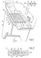
- a radiation detector of a tomography device provided with an interconnection device 1 according to the invention.
- This device allows the interconnection of the detection cells 2 of an X-ray tomography apparatus 3, with measurement channels not shown in this figure. These channels make it possible to view the image of an organ, on the basis of signals received from the detection cells, when the latter are subjected to X-ray radiation represented at R and having passed through the organ to be radiographed.
- the detection cells of the tomography device 3 are housed in a housing 4, one side of which, not shown, receives X-rays and the bottom 5 of which is closed by a cover 6.
- the interconnection device 1 has the form of a ribbon which passes through the housing at the interface 8 which separates the housing from its cover.
- This device 'interconnection comprises conductors 9 which will be described later in detail; -these conductors 9 are isolated from each other and are insulated from the housing, in particular by an insulating sheet 10 in which they may be embedded; this insulating sheet 10 is covered on each of its faces respectively by conductive layers 11, 12, themselves covered with insulating layers 13, 14.
- these conductive layers are brought to the polarization potential of the electrodes, in order to avoid the appearance of leakage currents in the insulation surrounding these conductors.
- These conductive layers act in the same way as a guard ring surrounding a threadlike conductor which would be brought to the same potential as this conductor.
- the interconnection device 1 can have the form shown in the figure, so as to cooperate with O-rings 15, 16 intended to ensure a perfect seal between the cover and the housing. It is obvious that the lateral portions 33 of the interconnection device only comprise, at the level of the housing, the insulating layers and plies and, possibly, only the conductive layers.
- the conductors are connected to the electrodes 7 in the manner shown at 32.
- this device comprises conductors 9 which are isolated from each other and which are isolated from the housing of the tomography apparatus, by virtue of a structure which comprises an insulating sheet 10 containing these conductors; this insulating sheet is covered on each of its faces respectively, by conductive layers 11, 12 themselves covered with insulating layers 13, 14.
- the conductors 9 are preferably parallel tapes made of copper by etching a continuous layer by example; the conductive layers 11, 12 can also be copper layers deposited on the faces of the sheet 10.
- This sheet 10 can consist of two layers 18, 19; layer 18, for example, initially carries the copper layer in which the conductive strips 9 are etched, which join each electrode to each electronic channel.
- the conductive layers 11, 12 are brought to the same polarization potential as that of the electrodes to which the conductors 9 are connected. These conductive layers 11, 12 act as guard rings between the conductive strips and the conductive mass of the housing of the tomography device.
- the insulating layers can be made of polytetrafluoroethylene, better known under the trade name of teflon, polyamide (“Kapton”) or epoxy reinforced with fiberglass.
- Fig. 3 provides a better understanding of the interconnection of the device according to the invention, between the detection cells 2 of an X-ray tomography device 3 and the measurement channels 20 and 27 of an electronic assembly 21 allowing a visualization of the organ radiographed by the tomography apparatus 3.
- This device can be of the same type as that described in the aforementioned patent application. It is assumed in this figure that the tomography apparatus is seen on its rear face and that the radiation R is perpendicular to the plane of the figure.
- This tomography device is of the multicellular type and the detection cells include a plurality of anodes 7 and cathodes 22 arranged alternately on insulating bars represented schematically at 23 and 24.
- the bars and the electrodes are arranged in the box 4, closed by the cover 6 held by screws 30.
- the sealing is ensured by means of the O-rings 15, 16 mentioned above. In this figure, only the seal 15 is visible.
- the insulating bars can be covered on their face opposite the ends of the electrodes which they support, with a conductive layer. These bars will be better described later.
- the electrodes 7 are for example brought to a positive bias potential with respect to a reference potential M, by virtue of an electrical supply 25, and constitute anodes.
- the electrodes such as 22 are brought to a negative bias potential with respect to a reference potential M, thanks to a power supply 26, and constitute cathodes.
- the measurement channels 27 are connected to the anodes 7 by the conductors 9 of the interconnection device 1 according to the invention.
- the interconnection device comprises, for the upper part of the device shown, conductors 9 embedded for example in the insulating layer 19 and covered by the insulating layer 18.
- the layers are also distinguished in the figure. conductors 11 and 12, themselves covered with insulating layers 13, 14.
- the conductive layers 11, 12 are carried by the conductor 42 at the same predetermined positive potential as that of the anodes 7, thanks to the power supply 25.
- the power supply 25 also allows on the one hand to apply this bias potential to the anodes 7 via the measurement channels 27, the circuit 32 and the conductors 9, and on the other hand to apply this potential to the conductive layer which covers the bars 23, which support the electrodes, as will be seen below in detail.
- the conductive layers 11 and 12 of the interconnection device which are continuous and brought to the same potential as the corresponding electrodes, act as a guard ring between the conductors 9 and the reference potential M to which the housing 4 of the tomography device 3.
- the interconnection device 1 makes it possible to connect the cathodes 22 to the measurement channels 20 of the electronic assembly 21, by means of the conductors 28, similar to the conductors 9 via the circuit 33.
- the negative potential of the power supply 26 is applied to the two conductive layers 11, 12 by the circuit 31.
- This negative bias potential is also applied via the measurement channels 20, of the circuit 33 and conductors 28 at each of the cathodes 22, as well as at the conductive layer covering the strip 24 which supports these cathodes, as will be seen below in detail.
- the conductive layers 11 and 12 follow the contour of the bottom of the housing 4, but they are of course interrupted in the middle part 40, 41 of this contour. Indeed, these conductive layers are brought to a positive potential in the upper part of the device (namely left part in the drawing) and to a negative potential in the lower part (right part in the drawing), for example.
- the insulating layers 13, 14, 18 and 19 are however continuous over the entire contour of the bottom of the housing 4.
- the bias potential of the anodes 7 is applied to these anodes by the circuit 32, which also serves to collect the measurement signals to be applied to the channels 27 of the electronic display assembly 21.
- the power supply 25 is connected to the positive inputs of the operational amplifiers 34, the negative inputs of which are connected to the circuit 32.
- the negative input of each operational amplifier is connected to the output of this amplifier via a feedback circuit 35 which can, for example, be a capacitor. These are the outputs 36 of these operational amplifiers which are connected to the display unit 5 of the assembly 21.
- the cathodes 22 are connected to the power supply 26 via the operational amplifiers 37.
- the negative input of each of these amplifiers is also connected to its output via a capacitor 38, by example.
- the outputs 39 of the amplifiers 37 are connected to the display unit 5.
- the overall resolution of the tomography device is double the resolution obtained in the case where only the cathodes are joined to the measurement channels. It is therefore possible, thanks to the interconnection device according to the invention, to use a tomography device which can have two parts; one of these parts can be intended for the visualization of an organ with a high spatial resolution and in this case, the anodes and the cathodes of this part are connected to the measurement channels; the other part can be intended for the display of an organ not requiring a high spatial resolution, in this case, only the cathodes are connected to the measurement channels of the electronic display assembly.
- FIG. 4 With reference to fig. 4, there is shown the tomography apparatus of FIG. 3, in section along a plane IV-IV perpendicular to the plane of FIG. 3. Only the upper part of the tomography apparatus (namely the right side part in the drawing) has been shown in this figure.
- the connection device according to the invention is shown at 1 in this figure.
- the conductors 9 are connected to the anodes 7, but it is obvious that in the lower part of the tomography apparatus, identical conductors 28 are connected to the cathodes.
- These conductors are, moreover, connected by connections 32 to the power supply 25, by means of operational amplifiers described above.
- This supply is that which allows the anodes to be brought to a positive bias voltage.
- the conductors 9 are embedded in the insulating layers 18, 19, themselves covered with the conductive layers 11, 12 connected at 42 to the power supply 25. These conductive layers are themselves covered by the insulating layers 13, 14.
- the layer conductive 12, as indicated above as well as in the aforementioned patent application, is connected at 43 to the conductive layers 45, 46, which cover the insulating bars supporting the anodes 7 which form a guard ring, at the base of these insulating bars .
- An electrical connection 47 makes it possible to bring the conductive layers covering the insulating bars supporting the anodes to the positive high voltage, at the bottom not shown of the tomography apparatus.
- connection device located at the lower part (not shown) of the tomography apparatus makes it possible to bring the cathodes 22 to a negative bias voltage and to apply this voltage via the electrical connection 48, to the conductive layers 49, 50 which cover the base of the bars supporting the cathodes.
- the interconnection device which has just been described has been assumed to be applied to the interconnection of the detection cells and of the measurement channels in an X-ray tomography apparatus in which all the electrodes are measurement electrodes. Therefore, the interconnection device has two symmetrical parts since it has two groups of conductors brought respectively to positive and negative potentials. If only the electrodes polarized by a positive high voltage, for example, serve as measurement electrodes, the device of the invention simply has one of the two symmetrical parts.
Landscapes
- Apparatus For Radiation Diagnosis (AREA)
- Measurement Of Radiation (AREA)
- Electron Tubes For Measurement (AREA)
- Connections Arranged To Contact A Plurality Of Conductors (AREA)
- Insulators (AREA)
- Measuring Leads Or Probes (AREA)
- Multi-Conductor Connections (AREA)
- Analysing Materials By The Use Of Radiation (AREA)
Description
La présente invention concerne un détecteur de radiation d'un appareil de tomographie qui comprend notamment une enceinte fermée par un couvercle, des électrodes de détection dans cette enceinte et des moyens d'interconnexion entre ces électrodes et des bornes conductrices extérieures à l'enceinte.The present invention relates to a radiation detector of a tomography device which comprises in particular an enclosure closed by a cover, detection electrodes in this enclosure and means of interconnection between these electrodes and conductive terminals external to the enclosure.
Ce détecteur s'applique plus particulièrement à un appareil de tomographie dans lequel il est nécessaire de prévoir un nombre important de connecteurs entre des électrodes contenues dans une enceinte fermée par un couvercle et des bornes conductrices extérieures à cette enceinte et dans lequel il est nécessaire d'éviter les courants de fuite entre ces connecteurs et les parties conductrices de l'enceinte et du couvercle.This detector applies more particularly to a tomography device in which it is necessary to provide a large number of connectors between electrodes contained in an enclosure closed by a cover and conductive terminals external to this enclosure and in which it is necessary to '' avoid leakage currents between these connectors and the conductive parts of the enclosure and cover.
On sait qu'un appareil de tomographie à rayons X comprend un détecteur constitué par des cellules de détection délimitées par des électrodes de mesure portées à un potentiel de polarisation et logées dans un boîtier dont une face reçoit les rayons X et dont le fond est fermé par un couvercle. Généralement, ce boîtier est rempli de gaz sous pression, tel que le xénon par exemple. Afin de pouvoir obtenir une image d'un organe observé grâce à l'appareil, il est nécessaire de connecter les cellules de détection à des voies électroniques de mesure des courants reçus par chaque électrode. Afin d'améliorer la résolution spatiale de l'appareil, il est nécessaire que le nombre de cellules de détection soit très important. Actuellement, ce nombre peut atteindre 500 et même 1000 cellules de détection. Le nombre des électrodes est bien entendu aussi important et dans un appareil présentant 500 à 1000 cellules de détection, 500 à 1000 connexions sont nécessaires pour relier l'appareil de tomographie aux différentes voies de mesure. Généralement, ces connexions sont réalisées par un câblage fil à fil, à la sortie du boîtier, et, afin d'isoler les différents fils du câblage et le boîtier, ces fils sortent du boîtier à travers des perles soudées ou collées sur ce boîtier. Le grand nombre d'électrodes nécessité par l'accroissement de la résolution spatiale rend difficile, voir même impossible, la disposition mécanique de 500 à 1000 perles de verre. Un exemple de réalisation d'un appareil de tomographie présentant un très grand nombre de cellules est donné dans la demande de brevet européen EP-A-10 474 avec priorité française du 13 octobre 1978 au nom du même demandeur. Ainsi qu'il apparaît dans cette demande de brevet, il est important d'éviter tout courant de fuite dans les isolants de l'appareil de tomographie. Dans l'interconnexion des cellules avec les voies de mesure, outre le problème posé par le grand nombre de conducteurs d'interconnexion de cellules avec des voies électroniques de mesure, un autre problème est posé par les courants de fuite qui apparaissent dans les traversées du boîtier et notamment lorsque des perles isolantes sont utilisées, tel que dans le brevet US-A-4 119 853. Ce brevet décrit un détecteur de radiation d'appareil de tomographie comportant une enceinte fermée par un couvercle démontable et des moyens d'interconnexion par des conducteurs entre les électrodes de détection contenues dans cette enceinte et l'extérieur, ces conducteurs se trouvant regroupés à l'intérieur de l'enceinte sous la forme d'un câble plat flexible, avant de déboucher à l'extérieur par l'intermédiaire de traverses isolantes montées dans le couvercle. Le câble plat flexible se compose de conducteurs noyés dans une nappe isolante insérée entre deux couches conductrices elles-mêmes insérées entre deux couches isolantes. Le détecteur décrit dans ce brevet ne permet pas, du fait des moyens de connexion qu'il utilise, d'éviter les courants de fuite qui apparaissent à la traversée de l'enceinte. Il ne permet pas non plus de relier un nombre important d'électrodes contenues dans l'enceinte, avec un grand nombre de bornes conductrices extérieures à cette enceinte, du fait de la présence des traverses isolantes encombrantes.It is known that an X-ray tomography device comprises a detector constituted by detection cells delimited by measurement electrodes brought to a polarization potential and housed in a housing one face of which receives X-rays and the bottom of which is closed by a cover. Generally, this box is filled with pressurized gas, such as xenon for example. In order to be able to obtain an image of an organ observed using the apparatus, it is necessary to connect the detection cells to electronic channels for measuring the currents received by each electrode. In order to improve the spatial resolution of the device, it is necessary that the number of detection cells is very large. Currently, this number can reach 500 and even 1000 detection cells. The number of electrodes is of course also large and in a device having 500 to 1000 detection cells, 500 to 1000 connections are necessary to connect the tomography device to the different measurement channels. Generally, these connections are made by wire-to-wire wiring, at the outlet of the housing, and, in order to isolate the various wires of the wiring and the housing, these wires exit from the housing through beads soldered or glued to this housing. The large number of electrodes required by the increase in spatial resolution makes it difficult, even impossible, the mechanical arrangement of 500 to 1000 glass beads. An exemplary embodiment of a tomography device having a very large number of cells is given in European patent application EP-A-10,474 with French priority of October 13, 1978 in the name of the same applicant. As it appears in this patent application, it is important to avoid any leakage current in the insulators of the tomography device. In the interconnection of cells with the measurement channels, in addition to the problem posed by the large number of cell interconnection conductors with electronic measurement channels, another problem is posed by the leakage currents which appear in the bushings of the housing and in particular when insulating beads are used, such as in patent US-A-4 119 853. This patent describes a radiation detector of tomography apparatus comprising an enclosure closed by a removable cover and means of interconnection by conductors between the detection electrodes contained in this enclosure and the outside, these conductors being grouped together inside the enclosure in the form of a flexible flat cable, before leading to the outside via insulating cross members mounted in the cover. The flexible flat cable consists of conductors embedded in an insulating sheet inserted between two conductive layers themselves inserted between two insulating layers. The detector described in this patent does not make it possible, due to the connection means which it uses, to avoid the leakage currents which appear when passing through the enclosure. It also does not make it possible to connect a large number of electrodes contained in the enclosure, with a large number of conductive terminals outside this enclosure, due to the presence of bulky insulating crosspieces.
Des moyens de connexion qui pourraient éventuellement permettre de relier un grand nombre d'électrodes intérieures à une enceinte d'un appareil de tomographie, avec un grand nombre de bornes conductrices extérieures à l'enceinte, est décrit dans le brevet FR-A-1 399 458. Ce brevet décrit un dispositif d'interconnexion par des conducteurs entre des bornes conductrices intérieures à une enceinte fermée par un couvercle démontable et des bornes conductrices extérieures à cette enceinte, dans lequel les conducteurs passent entre l'enceinte et le couvercle, ces conducteurs étant noyés dans une nappe de matériau isolant qui les isole électriquement entre eux et par rapport à l'enceinte et son couvercle. Ce dispositif permet de relier un grand nombre de bornes conductrices intérieures à une enceinte avec un grand nombre de bornes extérieures à cette enceinte. Il n'est toutefois pas destiné à résoudre un problème de courants de fuites à la traversée de l'enceinte.Connection means which could possibly make it possible to connect a large number of internal electrodes to an enclosure of a tomography apparatus, with a large number of conductive terminals external to the enclosure, is described in patent FR-A-1 399,458. This patent describes an interconnection device by conductors between conductive terminals inside an enclosure closed by a removable cover and conductive terminals outside this enclosure, in which the conductors pass between the enclosure and the cover, these conductors being embedded in a sheet of insulating material which electrically insulates them from each other and from the enclosure and its cover. This device makes it possible to connect a large number of internal conductive terminals to an enclosure with a large number of external terminals to this enclosure. However, it is not intended to solve a problem of leakage currents when crossing the enclosure.
L'invention a pour but de remédier aux inconvénients du détecteur de radiation décrit plus haut et notamment de réaliser un détecteur de radiation pour un appareil de tomographie dans lequel il est nécessaire de prévoir un nombre important de conducteurs entre des électrodes contenues dans une enceinte fermée par un couvercle et des bornes conductrices extérieures à cette enceinte, tout en évitant les courants de fuite entre ces conducteurs et les parties conductrices de l'enceinte et du couvercle. Ces buts sont atteints en noyant les conducteurs dans une nappe isolante entourée de couches conductrices portées au même potentiel que celui auquel sont portés les conducteurs. Ces couches conductrices sont elles-mêmes noyées dans des couches isolantes. Le détecteur de l'invention permet aussi d'éviter l'utilisation de perles isolantes entre l'enceinte et son couvercle.The object of the invention is to remedy the drawbacks of the radiation detector described above and in particular to produce a radiation detector for a tomography device in which it is necessary to provide a large number of conductors between electrodes contained in a closed enclosure. by a cover and conductive terminals outside this enclosure, while avoiding leakage currents between these conductors and the conductive parts of the enclosure and of the cover. These aims are achieved by embedding the conductors in an insulating sheet surrounded by conductive layers brought to the same potential as that to which the conductors are borne. These conductive layers are themselves embedded in insulating layers. The detector of the invention also makes it possible to avoid the use of insulating beads between the enclosure and its cover.
L'invention a pour objet un détecteur de radiation d'un appareil de tomographie, comprenant une enceinte fermée par un couvercle amovible, une pluralité d'électrodes de détection disposées dans ladite enceinte fermée, susceptibles de présenter des potentiels variables à mesurer, et des moyens pour interconnecter par des conducteurs lesdites électrodes de détection intérieures à ladite enceinte et des bornes conductrices extérieures à cette enceinte, caractérisé par le fait que lesdits moyens d'interconnexion présentent la forme d'un ruban passant entre l'enceinte et le couvercle, ledit ruban comprenant lesdits conducteurs noyés dans une nappe de matériau isolant qui les isole électriquement entre eux et par rapport à l'enceinte et son couvercle, ladite nappe de matériau isolant étant insérée entre deux couches conductrices, elles-mêmes insérées entre deux couches isolantes situées respectivement en regard de l'enceinte et du couvercle, lesdites électrodes étant destinées à être portées par l'intermédiaire desdits conducteurs à un potentiel de polarisation déterminé, et lesdites couches conductrices étant destinées à être portées au même potentiel de polarisation que lesdits conducteurs, afin d'éviter l'apparition de courants de fuite dans l'isolant entourant ces conducteurs.The subject of the invention is a radiation detector of a tomography device, comprising an enclosure closed by a removable cover, a plurality of detection electrodes disposed in said closed enclosure, capable of presenting variable potentials to be measured, and means for interconnecting by conductors said internal detection electrodes to said enclosure and conductive terminals outside this enclosure, characterized in that said interconnection means have the form of a ribbon passing between the enclosure and the cover, said tape comprising said conductors embedded in a sheet of insulating material which electrically insulates them from each other and with respect to the enclosure and its cover, said sheet of insulating material being inserted between two conductive layers, themselves inserted between two insulating layers located respectively facing the enclosure and the cover, said electrodes being intended to be worn by means of said conductors at a determined polarization potential, and said conductive layers being intended to be brought to the same polarization potential as said conductors, in order to avoid the appearance of leakage currents in the insulator surrounding these conductors.
Selon une autre caractéristique, ladite nappe isolante recouvre le pourtour de l'interface entre l'enceinte et le couvercle.According to another characteristic, said insulating sheet covers the periphery of the interface between the enclosure and the cover.
Selon une autre caractéristique, deux joints toriques d'étanchéité sont respectivement disposés en regard de l'une et l'autre faces de ladite nappe isolante.According to another characteristic, two sealing O-rings are respectively arranged opposite one and the other faces of said insulating sheet.
Selon une autre caractéristique, les conducteurs sont subdivisés en un premier et un second groupes insérés chacun séparément entre deux couches conductrices, les conducteurs desdits premier et second groupes étant destinés à être respectivement portés à un premier et à un second potentiels de polarisation et lesdites couches conductrices étant destinées à être respectivement portées au même potentiel de polarisation que celui du groupe de conducteurs correspondant.According to another characteristic, the conductors are subdivided into a first and a second group each inserted separately between two conductive layers, the conductors of said first and second groups being intended to be brought respectively to a first and to a second bias potential and said layers conductors being intended to be brought respectively to the same polarization potential as that of the corresponding group of conductors.
Enfin, selon une autre caractéristique, lesdites bornes conductrices extérieures à l'enceinte sont constituées par les bornes des voies de mesure de l'appareil de tomographie à rayons. D'autres caractéristiques et avantages de l'invention ressortiront mieux de la description qui va suivre, donnée en référence aux dessins annexés dans lesquels:
- - la fig. 1 représente un détecteur de radiation muni d'un dispositif d'interconnexion conforme à l'invention, permettant l'interconnexion des cellules de détection et des voies de mesure dans un appareil de tomographie à rayons X;
- - la fig. 2 est une vue en coupe transversale du dispositif d'interconnexion conforme à l'invention;
- - la fig. 3 est une vue schématique représentant le schéma électrique d'ensemble du dispositif d'interconnexion conforme à l'invention et de l'appareil de tomographie à rayons X;
- - la fig. 4 est une coupe schématique de l'appareil de tomographie de la fig. 3, selon un plan IV-IV perpendiculaire au plan de la fig. 3 faisant apparaître le dispositif d'interconnexion selon l'invention. Seule la partie supérieure de l'appareil de tomographie a été représentée sur cette coupe.
- - fig. 1 shows a radiation detector provided with an interconnection device according to the invention, allowing the interconnection of the detection cells and the measurement channels in an X-ray tomography apparatus;
- - fig. 2 is a cross-sectional view of the interconnection device according to the invention;
- - fig. 3 is a schematic view showing the overall electrical diagram of the interconnection device according to the invention and of the X-ray tomography apparatus;
- - fig. 4 is a schematic section of the tomography apparatus of FIG. 3, along a plane IV-IV perpendicular to the plane of FIG. 3 showing the interconnection device according to the invention. Only the upper part of the tomography device has been shown in this section.
Les mêmes éléments portent les mêmes références sur ces différentes figures.The same elements have the same references in these different figures.
En référence à la fig. 1, on a représenté un détecteur de radiation d'un appareil de tomographie muni d'un dispositif 1 d'interconnexion conforme à l'invention. Ce dispositif permet l'interconnexion des cellules de détection 2 d'un appareil 3 de tomographie à rayons X, avec des voies de mesure non représentées sur cette figure. Ces voies permettent de visualiser l'image d'un organe, à partir de signaux reçus des cellules de détection, lorsque celles-ci sont soumises à un rayonnement X représenté en R et ayant traversé l'organe à radiographier. Les cellules de détection de l'appareil de tomographie 3 sont logées dans un boîtier 4, dont une face non représentée reçoit les rayons X et dont le fond 5 est fermé par un couvercle 6. Ces cellules de détection comprennent des électrodes de mesure 7 qui peuvent être du même type que celles qui sont décrites dans la demande de brevet européen n° 10 474 précitée. Le dispositif 1 d'interconnexion a la forme d'un ruban qui traverse le boîtier à l'interface 8 qui sépare le boîtier de son couvercle. Ce dispositif 'd'interconnexion comprend des conducteurs 9 qui seront décrits plus loin en détail;-ces conducteurs 9 sont isolés les uns des autres et sont isolés du boîtier, notamment par une nappe isolante 10 dans laquelle ils peuvent être noyés; cette nappe isolante 10 est recouverte sur chacune de ses faces respectivement par des couches conductrices 11, 12, elles-mêmes recouvertes de couches isolantes 13, 14. Comme on le verra plus loin en détail, ces couches conductrices sont portées au potentiel de polarisation des électrodes, afin d'éviter l'apparition des courants de fuite dans l'isolant qui entoure ces conducteurs. Ces couches conductrices agissent de la même manière qu'un anneau de garde entourant un conducteur filiforme et qui serait porté au même potentiel que ce conducteur. Selon un mode de réalisation particulier et afin d'assurer une étanchéité parfaite entre le couvercle et le boîtier, au niveau de l'interface entre ce couvercle et ce boîtier, le dispositif d'interconnexion 1 peut avoir la forme représentée sur la figure, de manière à coopérer avec des joints toriques 15, 16 destinés à assurer une étanchéité parfaite entre le couvercle et le boîtier. Il est bien évident que les portions latérales 33 du dispositif d'interconnexion ne comportent au niveau du boîtier que les couches et nappes isolantes ainsi, éventuellement, que les couches conductrices. Les conducteurs sont reliés aux électrodes 7 de la manière représentée en 32.With reference to fig. 1, there is shown a radiation detector of a tomography device provided with an
En référence à la fig. 2, on a représenté en coupe transversale le dispositif d'interconnexion conforme à l'invention. Comme on l'a déjà indiqué dans la description relative à la fig. 1, ce dispositif comprend des conducteurs 9 qui sont isolés les uns des autres et qui sont isolés du boîtier de l'appareil de tomographie, grâce à une structure qui comprend une nappe isolante 10 renfermant ces conducteurs; cette nappe isolante est recouverte sur chacune de ses faces respectivement, par des couches conductrices 11, 12 elles-mêmes recouvertes de couches isolantes 13, 14. Les conducteurs 9 sont de préférence des rubans parallèles réalisés en cuivre par gravure d'une couche continue par exemple; les couches conductrices 11, 12 peuvent également être des couches de cuivre déposées sur les faces de la nappe 10. Cette nappe 10 peut être constituée de deux couches 18, 19; la couche 18 par exemple porte initialement la couche de cuivre dans laquelle sont gravées les bandes conductrices 9 qui réunissent chaque électrode à chaque voie électronique. Les couches conductrices 11, 12 sont portées au même potentiel de polarisation que celui des électrodes auxquelles les conducteurs 9 sont reliés. Ces couches conductrices 11, 12 jouent le rôle d'anneaux de garde entre les bandes conductrices et la masse conductrice du boîtier de l'appareil de tomographie. Les couches isolantes peuvent être réalisées en polytétrafluoréthylène, plus connu sous la dénomination commerciale de téflon, en polyamide («Kapton») ou en époxy armé de fibre de verre.With reference to fig. 2, there is shown in cross section the interconnection device according to the invention. As already indicated in the description relating to FIG. 1, this device comprises
La fig. 3 permet de mieux comprendre l'interconnexion du dispositif conforme à l'invention, entre les cellules 2 de détection d'un appareil 3 de tomographie à rayons X et les voies de mesure 20 et 27 d'un ensemble électronique 21 permettant une visualisation de l'organe radiographié grâce à l'appareil 3 de tomographie. Cet appareil peut être de même type que celui qui est décrit dans la demande de brevet précitée. On suppose sur cette figure que l'appareil de tomographie est vu sur sa face arrière et que le rayonnement R est perpendiculaire au plan de la figure. Cet appareil de tomographie est de type multicellulaire et les cellules de détection comprennent une pluralité d'anodes 7 et de cathodes 22 disposées de manière alternée sur des barrettes isolantes représentées schématiquement en 23 et 24. Les baret- tes et les électrodes sont disposées dans le boîtier 4, fermé par le couvercle 6 tenu par des vis 30. L'étanchéité est assurée grâce aux joints toriques 15, 16 mentionnés plus haut. Sur cette figure, seul est visible le joint 15. Comme indiqué dans la demande de brevet européen EP-A-10 474 précitée, les barrettes isolantes peuvent être recouvertes sur leur face en regard des extrémités des électrodes qu'elles supportent, d'une couche conductrice. Ces barrettes seront mieux décrites plus loin. Les électrodes 7 sont par exemple portées à un potentiel de polarisation positif par rapport à un potentiel de référence M, grâce à une alimentation électrique 25, et constituent des anodes. De la même manière, les électrodes telles que 22 sont portées à un potentiel négatif de polarisation par rapport à un potentiel de référence M, grâce à une alimentation électrique 26, et constituent des cathodes. Les voies de mesure 27 sont reliées aux anodes 7 par les conducteurs 9 du dispositif d'interconnexion 1 conforme à l'invention. Comme indiqué plus haut, le dispositif d'interconnexion comprend, pour la partie supérieure de l'appareil représenté, des conducteurs 9 noyés par exemple dans la couche isolante 19 et recouverts par la couche isolante 18. On distingue également sur la figure, les couches conductrices 11 et 12, elles-mêmes recouvertes des couches isolantes 13, 14. Les couches conductrices 11, 12 sont portées par le conducteur 42 au même potentiel positif prédéterminé que celui des anodes 7, grâce à l'alimentation 25. L'alimentation 25 permet par ailleurs d'une part d'appliquer ce potentiel de polarisation aux anodes 7 par l'intermédiaire des voies de mesure 27, du circuit 32 et des conducteurs 9, et d'autre part d'appliquer ce potentiel à la couche conductrice qui recouvre les barrettes 23, qui supportent les électrodes, comme on le verra plus loin en détail. Il en résulte que les couches conductrices 11 et 12 du dispositif d'interconnexion qui sont continues et portées au même potentiel que les électrodes correspondantes, jouent le rôle d'anneau de garde entre les conducteurs 9 et le potentiel de référence M auquel est porté le boîtier 4 de l'appareil de tomographie 3. De la même manière, le dispositif d'interconnexion 1 permet de relier les cathodes 22 aux voies de mesure 20 de l'ensemble électronique 21, par l'intermédiaire des conducteurs 28, semblables aux conducteurs 9 via le circuit 33. Le potentiel négatif de l'alimentation électrique 26 est appliqué aux deux couches conductrices 11, 12 par le circuit 31. Ce potentiel négatif de polarisation est également appliqué par l'intermédiaire des voies de mesure 20, du circuit 33 et des conducteurs 28 à chacune des cathodes 22, ainsi qu'à la couche conductrice recouvrant la barrette 24 qui supporte ces cathodes, comme on le verra plus loin en détail. Les couches conductrices 11 et 12 suivent le contour du fond du boîtier 4, mais elles sont bien entendu interrompues dans la partie médiane 40, 41 de ce contour. En effet, ces couches conductrices sont portées à un potentiel positif dans la partie haute de l'appareil (à savoir partie gauche au dessin) et à un potentiel négatif dans la partie basse (partie droite au dessin), par exemple. Les couches isolantes 13, 14, 18 et 19 sont par contre continues sur tout le contour du fond du boîtier 4.Fig. 3 provides a better understanding of the interconnection of the device according to the invention, between the
Le potentiel de polarisation des anodes 7 est appliqué à ces anodes par le circuit 32, qui sert aussi à recueillir les signaux de mesure à appliquer sur les voies 27 de l'ensemble électronique de visualisation 21. Pour appliquer une haute tension positive aux anodes 7 et recueillir les signaux de mesure sur ces anodes, l'alimentation 25 est reliée aux entrées positives des amplificateurs opérationnels 34, dont les entrées négatives sont reliées au circuit 32. L'entrée négative de chaque amplificateur opérationnel est relié à la sortie de cet amplificateur par l'intermédiaire d'un circuit de contre réaction 35 qui peut, par exemple, être un condensateur. Ce sont les sorties 36 de ces amplificateurs opérationnels qui sont reliées à l'unité de visualisation 5 de l'ensemble 21.The bias potential of the
De la même manière, les cathodes 22 sont reliées à l'alimentation 26 par l'intermédiaire des amplificateurs opérationnels 37. L'entrée négative de chacun de ces amplificateurs est également reliée à sa sortie par l'intermédiaire d'un condensateur 38, par exemple. Les sorties 39 des amplificateurs 37 sont reliées à l'unité de visualisation 5.In the same way, the
On a supposé sur cette figure que toutes les électrodes étaient des électrodes de mesure et que chaque électrode était donc réunie à une voie de mesure de l'ensemble électronique 21; il est bien évident cependant que seules les cathodes, par exemple, peuvent être reliées aux voies de mesure tandis que les anodes sont simplement portées à un potentiel positif de polarisation, sans être reliées à une voie de mesure. Dans ce cas, les anodes sont réunies entre elles et portées au potentiel positif de polarisation tandis que les cathodes sont réunies aux voies de mesure. Ces voies de mesure sont référencées à un potentiel négatif V par rapport à une masse de référence M, dont le potentiel est zéro volt. Le potentiel des électrodes, en l'absence de signal, est V. Il est bien évident que dans le cas où les voies de mesure sont reliées aux anodes et aux cathodes, la résolution globale de l'appareil de tomographie est double de la résolution obtenue dans le cas où seules les cathodes sont réunies aux voies de mesure. Il est donc possible, grâce au dispositif d'interconnexion conforme à l'invention, d'utiliser un appareil de tomographie pouvant présenter deux parties; l'une de ces parties peut être destinée à la visualisation d'un organe avec une résolution spatiale élevée et dans ce cas, les anodes et les cathodes de cette partie sont reliées aux voies de mesure; l'autre partie peut être destinée à la visualisation d'un organe ne nécessitant pas une résolution spatiale élevée, dans ce cas, seules les cathodes sont reliées aux voies de mesure de l'ensemble électronique de visualisation.It has been assumed in this figure that all the electrodes were measurement electrodes and that each electrode was therefore joined to a measurement channel of the
En référence à la fig. 4, on a représenté l'appareil de tomographie de la fig. 3, en coupe selon un plan IV-IV perpendiculaire au plan de la fig. 3. Seule la partie supérieure de l'appareil de tomographie (à savoir partie latérale droite au dessin) a été représentée sur cette figure. Le dispositif de connexion conforme à l'invention est représenté en 1 sur cette figure. Les conducteurs 9 sont reliés aux anodes 7, mais il est bien évident que dans la partie inférieure de l'appareil de tomographie, des conducteurs identiques 28 sont reliés aux cathodes. Ces conducteurs sont, en outre, reliés par des connexions 32 à l'alimentation 25, par l'intermédiaire d'amplificateurs opérationnels décrits plus haut.With reference to fig. 4, there is shown the tomography apparatus of FIG. 3, in section along a plane IV-IV perpendicular to the plane of FIG. 3. Only the upper part of the tomography apparatus (namely the right side part in the drawing) has been shown in this figure. The connection device according to the invention is shown at 1 in this figure. The
Cette alimentation est celle qui permet de porter les anodes à une tension de polarisation positive. Les conducteurs 9 sont noyés dans les couches isolantes 18, 19, elles-mêmes recouvertes des couches conductrices 11, 12 reliées en 42 à l'alimentation 25. Ces couches conductrices sont elles-mêmes recouvertes par les couches isolantes 13, 14. La couche conductrice 12, comme indiqué plus haut ainsi que dans la demande de brevet précitée, est reliée en 43 aux couches conductrices 45, 46, qui recouvrent les barrettes isolantes supportant les anodes 7 qui forment un anneau de garde, à la base de ces barrettes isolantes. Une liaison électrique 47 permet de porter à la haute tension positive les couches conductrices recouvrant les barrettes isolantes supportant les anodes, à la partie inférieure non représentée de l'appareil de tomographie. De la même manière, le dispositif de connexion situé à la partie inférieure (non représentée) de l'appareil de tomographie, permet de porter les cathodes 22 à une tension de polarisation négative et d'appliquer cette tension par la liaison électrique 48, aux couches conductrices 49, 50 qui recouvrent la base des barrettes supportant les cathodes.This supply is that which allows the anodes to be brought to a positive bias voltage. The
Le dispositif d'interconnexion qui vient d'être décrit a été supposé appliqué à l'interconnexion des cellules de détection et des voies de mesure dans un appareil de tomographie à rayons X dont toutes les électrodes sont des électrodes de mesure. De ce fait, le dispositif d'interconnexion présente deux parties symétriques puisqu'il présente deux groupes de conducteurs portés respectivement à des potentiels positif et négatif. Si seules les électrodes polarisées par une haute tension positive par exemple servent d'électrodes de mesure, le dispositif de l'invention présente simplement l'une des deux parties symétriques.The interconnection device which has just been described has been assumed to be applied to the interconnection of the detection cells and of the measurement channels in an X-ray tomography apparatus in which all the electrodes are measurement electrodes. Therefore, the interconnection device has two symmetrical parts since it has two groups of conductors brought respectively to positive and negative potentials. If only the electrodes polarized by a positive high voltage, for example, serve as measurement electrodes, the device of the invention simply has one of the two symmetrical parts.
Claims (5)
Applications Claiming Priority (2)
| Application Number | Priority Date | Filing Date | Title |
|---|---|---|---|
| FR7833545A FR2443184A1 (en) | 1978-11-28 | 1978-11-28 | DEVICE FOR INTERCONNECTING BY CONDUCTORS BETWEEN CONDUCTIVE TERMINALS LOCATED WITHIN A DISMOUNTABLE CLOSED ENCLOSURE AND CONDUCTIVE TERMINALS EXTERNAL TO THE SAME |
| FR7833545 | 1978-11-28 |
Publications (2)
| Publication Number | Publication Date |
|---|---|
| EP0012065A1 EP0012065A1 (en) | 1980-06-11 |
| EP0012065B1 true EP0012065B1 (en) | 1984-04-18 |
Family
ID=9215443
Family Applications (1)
| Application Number | Title | Priority Date | Filing Date |
|---|---|---|---|
| EP79400892A Expired EP0012065B1 (en) | 1978-11-28 | 1979-11-20 | Radiation detector for a tomographic apparatus |
Country Status (5)
| Country | Link |
|---|---|
| US (1) | US4297576A (en) |
| EP (1) | EP0012065B1 (en) |
| JP (1) | JPS5581474A (en) |
| DE (1) | DE2966929D1 (en) |
| FR (1) | FR2443184A1 (en) |
Families Citing this family (12)
| Publication number | Priority date | Publication date | Assignee | Title |
|---|---|---|---|---|
| JPS57161677A (en) * | 1981-03-31 | 1982-10-05 | Toshiba Corp | Radiation detector |
| DE3114692A1 (en) * | 1981-04-10 | 1982-10-28 | Siemens AG, 1000 Berlin und 8000 München | BEAM DETECTOR |
| FR2505492B1 (en) * | 1981-05-06 | 1985-11-08 | Commissariat Energie Atomique | |
| US4490614A (en) * | 1982-04-30 | 1984-12-25 | Interad Systems, Inc. | Housing for an ionization detector array in a tomographic scanner |
| NL8202258A (en) * | 1982-06-04 | 1984-01-02 | Philips Nv | DEVICE WITH MULTIPLE ELECTRICAL TRANSITION. |
| US4528449A (en) * | 1982-12-27 | 1985-07-09 | Honeywell Inc. | Detector dewar assembly |
| JPH081797B2 (en) * | 1983-07-30 | 1996-01-10 | 株式会社日立製作所 | Radiation detector |
| US4763008A (en) * | 1983-12-27 | 1988-08-09 | General Electric Company | Ionization detector with conductive signal and ground traces |
| US4570071A (en) * | 1983-12-27 | 1986-02-11 | General Electric Company | Ionization detector |
| US5010252A (en) * | 1983-12-27 | 1991-04-23 | General Electric Company | Ionization detector |
| GB2179784B (en) * | 1985-08-30 | 1989-12-06 | Philips Electronic Associated | Cathode ray tubes |
| FR2626379B1 (en) * | 1988-01-26 | 1990-05-11 | Commissariat Energie Atomique | DETECTOR FOR X-RAY TOMOGRAPHY |
Citations (1)
| Publication number | Priority date | Publication date | Assignee | Title |
|---|---|---|---|---|
| US4119853A (en) * | 1977-06-09 | 1978-10-10 | General Electric Company | Multicell X-ray detector |
Family Cites Families (5)
| Publication number | Priority date | Publication date | Assignee | Title |
|---|---|---|---|---|
| FR1399458A (en) * | 1964-06-25 | 1965-05-14 | Burndy Corp | Connector with folded contact |
| US3774232A (en) * | 1971-11-11 | 1973-11-20 | Circuit Stik Inc | Package for integrated circuit chip |
| JPS5137899B2 (en) * | 1973-05-25 | 1976-10-19 | ||
| US4217498A (en) * | 1976-09-13 | 1980-08-12 | General Electric Company | Tomographic scanning apparatus with ionization detector means |
| US4161655A (en) * | 1977-11-28 | 1979-07-17 | General Electric Company | Multi-cell detector using printed circuit board |
-
1978
- 1978-11-28 FR FR7833545A patent/FR2443184A1/en active Granted
-
1979
- 1979-11-20 DE DE7979400892T patent/DE2966929D1/en not_active Expired
- 1979-11-20 EP EP79400892A patent/EP0012065B1/en not_active Expired
- 1979-11-23 US US06/097,051 patent/US4297576A/en not_active Expired - Lifetime
- 1979-11-28 JP JP15414679A patent/JPS5581474A/en active Granted
Patent Citations (1)
| Publication number | Priority date | Publication date | Assignee | Title |
|---|---|---|---|---|
| US4119853A (en) * | 1977-06-09 | 1978-10-10 | General Electric Company | Multicell X-ray detector |
Also Published As
| Publication number | Publication date |
|---|---|
| FR2443184A1 (en) | 1980-06-27 |
| DE2966929D1 (en) | 1984-05-24 |
| EP0012065A1 (en) | 1980-06-11 |
| FR2443184B1 (en) | 1982-07-09 |
| US4297576A (en) | 1981-10-27 |
| JPS5581474A (en) | 1980-06-19 |
| JPS649709B2 (en) | 1989-02-20 |
Similar Documents
| Publication | Publication Date | Title |
|---|---|---|
| EP0012065B1 (en) | Radiation detector for a tomographic apparatus | |
| FR2561020A1 (en) | MULTI-LAYER MATRIX LIQUID CRYSTAL DISPLAY DEVICE | |
| FR2618939A1 (en) | ASSEMBLED CABLE FOR ELECTRICAL SIGNAL TRANSMISSION SYSTEM | |
| WO1994023648A1 (en) | Sensor device for electrocardiogram | |
| FR2681444A1 (en) | ELECTROCHROME DEVICE. | |
| FR2725072A1 (en) | ELECTRICAL PROTECTION OF A FLAT DISPLAY ANODE | |
| EP0007842A1 (en) | Device for the detection and localization of radiation | |
| EP0531190B1 (en) | X-ray unit with high-voltage power supply device integrated in the housing | |
| EP0064913B1 (en) | X-rays multidetector | |
| FR2572183A1 (en) | METHOD AND APPARATUS FOR VERIFICATION BY MEASURING IMPEDANCE OF THE ELECTRIC CONTINUITY OF AN ELECTRICALLY CONDUCTIVE MATERIAL DEVICE | |
| EP0729128A2 (en) | Apparatus for addressing an electrode of a microtip display panel | |
| FR2638568A1 (en) | SOLAR PANEL ANTI-ELECTRICITY STATIC | |
| FR2606213A1 (en) | A NEW COMPOSITE MATERIAL OF FLEXIBLE PREFERENCE, MEASURING DEVICE FORMING A COMBINED FLOWMETER AND TEMPERATURE SENSOR COMPRISING SUCH A COMPOSITE MATERIAL AND METHOD OF PREPARING SUCH A MATERIAL | |
| FR2509053A1 (en) | DEVICE FOR DETECTING WATER INTAKE WITHIN A SEISMIC FLUTE | |
| FR2517864A1 (en) | DEVICE FOR RECORDING AND READING IMAGES | |
| EP0046125B1 (en) | Radiation detector | |
| EP2224252B1 (en) | Capacitive measuring devise for a high voltage element | |
| FR2507317A1 (en) | PYROELECTRIC DETECTOR AND METHOD OF OPERATION | |
| EP0326479B1 (en) | Detector for x-ray tomography | |
| FR2848027A1 (en) | PHOTOELECTRIC DETECTION DEVICE AND METHOD FOR PRODUCING THE SAME | |
| FR2633730A1 (en) | DEVICE FOR VISUALIZING THERMAL RADIATIONS AND SYSTEMS COMPRISING SUCH DEVICES | |
| FR3060241A1 (en) | PHOTOVOLTAIC MODULE AND PANEL OF INTERCONNECTED PHOTOVOLTAIC MODULES | |
| EP2363876B1 (en) | Ionising radiation detector | |
| FR2806807A1 (en) | RADIATION DETECTOR WITH SEMICONDUCTOR JUNCTION FOR MEASURING HIGH FLOW RATES OF X OR GAMMA RADIATION | |
| EP2252900B1 (en) | Device for modeling a solar panel for use in space |
Legal Events
| Date | Code | Title | Description |
|---|---|---|---|
| PUAI | Public reference made under article 153(3) epc to a published international application that has entered the european phase |
Free format text: ORIGINAL CODE: 0009012 |
|
| AK | Designated contracting states |
Designated state(s): DE GB NL |
|
| 17P | Request for examination filed |
Effective date: 19801108 |
|
| GRAA | (expected) grant |
Free format text: ORIGINAL CODE: 0009210 |
|
| AK | Designated contracting states |
Designated state(s): DE GB NL |
|
| REF | Corresponds to: |
Ref document number: 2966929 Country of ref document: DE Date of ref document: 19840524 |
|
| PLBI | Opposition filed |
Free format text: ORIGINAL CODE: 0009260 |
|
| 26 | Opposition filed |
Opponent name: SIEMENS AKTIENGESELLSCHAFT, BERLIN UND MUENCHEN Effective date: 19840720 |
|
| PLBN | Opposition rejected |
Free format text: ORIGINAL CODE: 0009273 |
|
| STAA | Information on the status of an ep patent application or granted ep patent |
Free format text: STATUS: OPPOSITION REJECTED |
|
| 27O | Opposition rejected |
Effective date: 19861120 |
|
| NLR2 | Nl: decision of opposition | ||
| PGFP | Annual fee paid to national office [announced via postgrant information from national office to epo] |
Ref country code: DE Payment date: 19911029 Year of fee payment: 13 |
|
| PGFP | Annual fee paid to national office [announced via postgrant information from national office to epo] |
Ref country code: GB Payment date: 19911119 Year of fee payment: 13 |
|
| PGFP | Annual fee paid to national office [announced via postgrant information from national office to epo] |
Ref country code: NL Payment date: 19911130 Year of fee payment: 13 |
|
| PG25 | Lapsed in a contracting state [announced via postgrant information from national office to epo] |
Ref country code: GB Effective date: 19921120 |
|
| PG25 | Lapsed in a contracting state [announced via postgrant information from national office to epo] |
Ref country code: NL Effective date: 19930601 |
|
| GBPC | Gb: european patent ceased through non-payment of renewal fee |
Effective date: 19921120 |
|
| NLV4 | Nl: lapsed or anulled due to non-payment of the annual fee | ||
| PG25 | Lapsed in a contracting state [announced via postgrant information from national office to epo] |
Ref country code: DE Effective date: 19930803 |