EP0002790A2 - Appareil de mesure pour l'analyse en fréquence des niveaux de signaux électriques dans une large gamme d'amplitudes - Google Patents
Appareil de mesure pour l'analyse en fréquence des niveaux de signaux électriques dans une large gamme d'amplitudes Download PDFInfo
- Publication number
- EP0002790A2 EP0002790A2 EP78101772A EP78101772A EP0002790A2 EP 0002790 A2 EP0002790 A2 EP 0002790A2 EP 78101772 A EP78101772 A EP 78101772A EP 78101772 A EP78101772 A EP 78101772A EP 0002790 A2 EP0002790 A2 EP 0002790A2
- Authority
- EP
- European Patent Office
- Prior art keywords
- amplifier
- frequency
- control
- measuring device
- adder
- Prior art date
- Legal status (The legal status is an assumption and is not a legal conclusion. Google has not performed a legal analysis and makes no representation as to the accuracy of the status listed.)
- Granted
Links
Images


Classifications
-
- G—PHYSICS
- G01—MEASURING; TESTING
- G01R—MEASURING ELECTRIC VARIABLES; MEASURING MAGNETIC VARIABLES
- G01R23/00—Arrangements for measuring frequencies; Arrangements for analysing frequency spectra
- G01R23/16—Spectrum analysis; Fourier analysis
-
- G—PHYSICS
- G01—MEASURING; TESTING
- G01R—MEASURING ELECTRIC VARIABLES; MEASURING MAGNETIC VARIABLES
- G01R19/00—Arrangements for measuring currents or voltages or for indicating presence or sign thereof
- G01R19/0007—Frequency selective voltage or current level measuring
-
- H—ELECTRICITY
- H04—ELECTRIC COMMUNICATION TECHNIQUE
- H04B—TRANSMISSION
- H04B3/00—Line transmission systems
- H04B3/02—Details
- H04B3/46—Monitoring; Testing
- H04B3/48—Testing attenuation
Definitions
- the invention relates to a measuring device for a frequency analysis of signal levels within a large dynamic range, consisting of a frequency conversion device with a synthesizer that generates the conversion frequencies in a controllable manner, an intermediate frequency amplifier arrangement with adjustable gain and a signal level evaluation and display device.
- Frequency analyzers of this type can be used, for example, in measuring devices which are used to track down small transmitters for monitoring purposes.
- Another field of application is the measurement of terrestrial radiation. Flying objects or spacecraft are particularly suitable for the systematic exploration of electromagnetic radiation within a wide frequency range. In this case, the relatively fast movement that is carried out by spacecraft, in particular satellites, requires a receiving system that ensures maximum resolution in the frequency and level range in extremely short times - up to the physical limits.
- the quality of the measurement results is in other words essentially determined by the achievable geographic, frequency and level resolution of the radio frequency power density spectrum to be examined.
- the local resolving power is largely given by the orbital data of the spacecraft and the antenna bundling.
- the frequency resolution is determined by the available measuring time and the radio frequency bandwidth to be scanned.
- the level resolution depends on the expected power density of the radiation at the receiver input and on the minimum measurable input level, based on the minimum intermediate frequency bandwidth.
- the required minimum dwell time at a certain frequency is essentially determined by the intermediate frequency bandwidth used (settling) and the time required to measure the level (large dynamic range).
- the quality of the measurement results can only be optimized by keeping the required minimum dwell time at a specific frequency as short as possible .
- the invention has for its object to provide a solution for a measuring device for carrying out an extremely fast frequency analysis of signal levels within a large dynamic range, which allows extremely fast automatic level measurement with high selection properties.
- the intermediate frequency amplifier arrangement has two or more selective amplifiers arranged one behind the other with automatic gain control, the bandwidth of which is reduced in the direction of the received signal level to be amplified from amplifier to amplifier, and further that the control variables occurring in the individual amplifiers are added up in an adder, taking into account the predetermined control characteristics are and that the total value is supplied from the output of the adder to the signal evaluation and display device.
- the invention is based on the finding that the speed of the level measurement in a large dynamic range can be designed extremely quickly if only the last selective amplifier is set with regard to its selectivity for the desired frequency resolution. In this way it is in fact possible to design the multi-stage control required in the case of a large dynamic range in such a way that the control time is practically determined by the control of the last amplifier having the highest selectivity.
- the synthesizer makes sense to control the synthesizer for a sudden frequency change in stages, the size of which is the bandwidth of the selective amplifier present in the course of the amplification of the received signal level, which has the spectral resolution specifies, is adjusted.
- the sum value at the output of the adder is fed to the signal level evaluation and display device in time with the frequency change of the synthesizer.
- the signal level evaluation and display device has an analog-digital converter on the input side, which is also controlled in time with the frequency change of the synthesizer.
- the conditions are particularly favorable if the control of the amplifiers each have a logarithmic-linear characteristic and the adder is designed for a linear summation.
- the automatic gain control of the selective amplifiers has a controllable attenuator arranged between two amplifier stages.
- the control loop comprising the attenuator, a control amplifier with a second output for the adder and an amplifier stage is designed to be broadband.
- the control loop does not contain the selective network that determines the selectivity of the selective amplifier, so that the control works extremely quickly.
- each control amplifier has a suitably dimensioned response threshold.
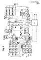
- the synthesizer 1, which is connected with its input E to the antenna of a spacecraft and receives a signal spectrum related thereto depending on its spatial orientation, is on the input side with a lock Sp for the on-board transmitter in the frequency range from 2 to 2 , 3 GHz and a broadband preamplifier V with a subsequent bandpass filter BP for the frequency range to be examined from 0.1 to 1 GHz.
- the amplified signal is fed to the converter U1.
- the converter U1 receives its conversion oscillation from the synthesizer synth controlled by the control device ST. Within the cycle clock ZT supplied to the control device St, the synthesizer changes its frequency 90,000 times in steps of 10 kHz and thus determines the frequency resolution of the signal spectrum in the range between 0.1 and 1 GHz.
- the synthesizer also has a switch s which, in the time domain of the transition from one frequency to the next, connects
- the converter U1 converts the signal fed to it into the first intermediate frequency of 3.5 GHz.
- This intermediate frequency signal is fed to the selective amplifier SV1
- the selective network has a bandwidth of 6 MHz.
- the amplifier has a total of three amplifier stages.
- the attenuator puts together with the third amplifier stage and the control amplifier represent an automatically operating level controller.
- the control amplifier RV1 has a response threshold above which it controls the controllable attenuator PR1 from its minimum attenuation towards its maximum attenuation. Furthermore, the control amplifier RV1 has a second output, via which it is connected to one of the three inputs of the adder Ad.
- the selective amplifier SV1 is followed by a second converter U2, which converts the intermediate frequency signal at 3.5 GHz to a second intermediate frequency position of 10.7 MHz.
- the intermediate frequency signal of 10.7 MHz is fed to the second selective amplifier SV2, which is constructed like the selective amplifier SV1.
- the controllable attenuator is labeled PR2 and the control amplifier RV2.
- a second output of the control amplifier is in turn connected to the second input of the adder Ad.
- the bandwidth b of the selective network of this second selective amplifier SV2 is 100 kHz here.
- a third converter U3 follows, which converts the signal to the third intermediate frequency position of 455 kHz.
- the control amplifiers RV1, RV2, RV3 have a logarithmic-linear characteristic, so that at the output of the adder Ad the sum of the control variables of these amplifiers, which corresponds to the level value of the frequency signal component determined in each case, also occurs logarithmically-linear.
- the adder Ad is followed by an analog-digital converter A / D, the digital output signal of which is fed to the signal level evaluation and display device AA.
- the curves MIN and MAX indicate the level curve at which the minimum or maximum level of the frequency-related signal component to be measured occurs at the input E in the frequency interval of 10 kHz.
- the dash-dotted line indicates the response wave Vo of the control amplifier, to which the signal at the output A of the third selective amplifier SV3 according to FIG. 1 is regulated.
- the curve shape Z shown in broken line indicates the case in which further strong spectral lines are present in neighboring regions of the frequency interval of 10 kHz just selected. Because of the lower selectivity of the first and second selective amplifiers SV1 and SV2, they of course come into play first and are only suppressed in the last 'selective amplifier SV3.
- the circuit diagram of the synthesizer shown in more detail in FIG. 3 shows a controllable oscillator VCO for the frequency range from 2.5 to 3.4 GHz, the actual output of which is connected to the converter U1 via the switch s already shown in FIG. 1.
- the control loop for this controllable oscillator comprises a total of four consecutive mixers M1 to M4, a phase comparator ⁇ 1 and a loop filter TP in the form of a low-pass filter with a cut-off frequency of 3 MHz.
- the synthesizer contains two frequency multiplier arrangements connected in series, of which the first frequency multiplier arrangement with the frequency multipliers FV11 'to 13 from the normal frequency Fo the frequencies 700, 800 and 900 MHz and the second group of frequency multipliers with the frequency multipliers FV21 to FV23 the frequencies 2100, 2400 and derive 2700 MHz.
- the frequencies 2100, 2400 and 2700 MHz can be switched on using the switch s2 the mixer M1 are applied, at whose first input the output oscillation of the oscillator VCO is present.
- the frequencies between 400 and 700 MHz generated by this mixer are mixed down in the second mixer M2 with one of the frequencies 700, 800 and 900 MHz that can be switched on via the switch s2 in the frequency range from 200 to 300 MHz.
- these frequencies between 30 and 40 MHz are connected to one of the output vibrations of the synthesizers SynthI to SynthIII, which can be alternately switched on via the switch s3.
- the synthesizers SynthI to SynthIII are constructed analogously to the auxiliary oscillator VC02 shown below, which is provided with a phase locked loop. They differ from this only in that the fixed frequency divider FT1 is omitted and the normal frequency fo "is supplied to each of these synthesizers as a reference frequency. All three synthesizers also generate an output oscillation in the frequency range between 30 and 40 MHz and are always switched on in succession via the switch s3.
- the overall circuit is controlled by means of the control device St, which in turn is supplied with the cycle clock ZT and the normal frequency fo, such that the oscillator VCO during a cycle of the cycle clock ZT over the frequency range of 900 MHz, starting from 3.4 GHz in simultaneous stages is switched from 10 kHz.
- the block diagram of the control device St shown in FIG. 4 has the clock generator TG, to which two signals which are synchronous with one another, the cycle clock ZT and the normal frequency fo are supplied. From this, the clock generator derives an oscillation with the fundamental frequency fg, which, based on the exemplary embodiment of the synthesizer according to FIG. 3 and assuming a cycle time of 32 seconds, is 2816 Hz. This results in a switchover cycle for the generation of 90,000 frequency values within a cycle time, which is 355 ⁇ sec at intervals of 10 kHz steps in succession. In the rhythm of the basic frequency fg, the switch s is opened briefly in order to bridge the switchover time of the synthesizer, as has already been explained. Furthermore, the switch s3 according to FIG. 3 is controlled with this basic frequency fg in such a way that the synthesizers SynthI to III are switched on to the phase comparator g1 in constant change in this rhythm.
- the output of the clock generator TG is followed by the three-decade counter Z3D, the digital outputs of which are alternately connected to the control inputs via the switch s4, which is also controlled with the fundamental frequency fg Synthesizer SynthI to III are turned on.
- the three-decade counter Z3D As soon as the three-decade counter Z3D has reached its end position, it emits a pulse to the one-decade counter Z1D connected after it. At the same time, this pulse brings it back to its starting position via the reset input R.
- the one-decade counter Z1D digitally controls the variable frequency divider FT2 via its outputs, which is arranged in the control loop of the auxiliary oscillator VC02.
- the one-decade counter As soon as the one-decade counter has reached its end position, it emits an impulse which is effective in three ways. First, it switches the one-decade counter Z1D back to its starting position via the reset input R; second, it controls the switch s2 according to FIG. 3 and, thirdly, it controls the switch s1 via the frequency divider FT3.
Landscapes
- Physics & Mathematics (AREA)
- General Physics & Mathematics (AREA)
- Engineering & Computer Science (AREA)
- Computer Networks & Wireless Communication (AREA)
- Signal Processing (AREA)
- Mathematical Physics (AREA)
- Amplifiers (AREA)
- Measuring Frequencies, Analyzing Spectra (AREA)
- Stabilization Of Oscillater, Synchronisation, Frequency Synthesizers (AREA)
- Measurement Of Resistance Or Impedance (AREA)
- Testing Electric Properties And Detecting Electric Faults (AREA)
- Radar Systems Or Details Thereof (AREA)
- Superheterodyne Receivers (AREA)
Applications Claiming Priority (2)
| Application Number | Priority Date | Filing Date | Title |
|---|---|---|---|
| DE2758154A DE2758154C3 (de) | 1977-12-27 | 1977-12-27 | Meßeinrichtung für eine Frequenzanalyse von Signalpegeln innerhalb eines großen Dynamikbereiches |
| DE2758154 | 1977-12-27 |
Publications (3)
| Publication Number | Publication Date |
|---|---|
| EP0002790A2 true EP0002790A2 (fr) | 1979-07-11 |
| EP0002790A3 EP0002790A3 (en) | 1979-07-25 |
| EP0002790B1 EP0002790B1 (fr) | 1983-10-19 |
Family
ID=6027378
Family Applications (1)
| Application Number | Title | Priority Date | Filing Date |
|---|---|---|---|
| EP78101772A Expired EP0002790B1 (fr) | 1977-12-27 | 1978-12-19 | Appareil de mesure pour l'analyse en fréquence des niveaux de signaux électriques dans une large gamme d'amplitudes |
Country Status (7)
| Country | Link |
|---|---|
| US (1) | US4232263A (fr) |
| EP (1) | EP0002790B1 (fr) |
| JP (1) | JPS54106277A (fr) |
| CA (1) | CA1123056A (fr) |
| DE (1) | DE2758154C3 (fr) |
| IE (1) | IE47705B1 (fr) |
| NO (1) | NO150979C (fr) |
Cited By (3)
| Publication number | Priority date | Publication date | Assignee | Title |
|---|---|---|---|---|
| FR2474174A1 (fr) * | 1980-01-21 | 1981-07-24 | Tektronix Inc | Analyseur de formes d'ondes a comparateur |
| EP0454946A1 (fr) * | 1990-05-03 | 1991-11-06 | Landis & Gyr Business Support AG | Procédé pour déterminer de valeurs d'approximation des valeurs instantanées de paramètres d'un signal sinusoidal avec fréquence constante et connue |
| RU208335U1 (ru) * | 2021-09-13 | 2021-12-14 | Федеральное государственное унитарное предприятие «Всероссийский научно-исследовательский институт автоматики им.Н.Л.Духова» (ФГУП «ВНИИА») | Блок измерения частоты следования импульсов |
Families Citing this family (1)
| Publication number | Priority date | Publication date | Assignee | Title |
|---|---|---|---|---|
| US4802098A (en) * | 1987-04-03 | 1989-01-31 | Tektronix, Inc. | Digital bandpass oscilloscope |
Citations (4)
| Publication number | Priority date | Publication date | Assignee | Title |
|---|---|---|---|---|
| FR1373665A (fr) * | 1963-02-13 | 1964-10-02 | Cit Alcatel | Mesureur de champ radioélectrique, de construction simplifiée |
| DE1516739A1 (de) * | 1966-06-25 | 1969-07-10 | Braun Ag | Abstimmanzeige bei Rundfunkempfangsgeraeten mit sehr grossem Regelumfang |
| FR2068716A1 (fr) * | 1969-11-29 | 1971-08-27 | Grundig Emv | |
| DE2119898A1 (de) * | 1971-04-23 | 1972-11-02 | Wandel U. Goltermann, 7410 Reutlingen | Selektiver Pegelmesser mit mindestens zweimaliger Frequenzumsetzung und mit Kalibriereinrichtung |
Family Cites Families (4)
| Publication number | Priority date | Publication date | Assignee | Title |
|---|---|---|---|---|
| US3470468A (en) * | 1965-07-06 | 1969-09-30 | Melpar Inc | Synthesis and wave generation with compactly carried waveforms |
| US3418574A (en) * | 1966-01-28 | 1968-12-24 | Raytheon Co | Spectrum analyzer using limited operating frequency bandwidth |
| US4005417A (en) * | 1975-08-14 | 1977-01-25 | Raytheon Company | Frequency spectrum analyzer |
| US3971927A (en) * | 1975-11-03 | 1976-07-27 | The United States Of America As Represented By The Secretary Of The Navy | Modular discrete cosine transform system |
-
1977
- 1977-12-27 DE DE2758154A patent/DE2758154C3/de not_active Expired
-
1978
- 1978-12-19 EP EP78101772A patent/EP0002790B1/fr not_active Expired
- 1978-12-19 US US05/971,006 patent/US4232263A/en not_active Expired - Lifetime
- 1978-12-22 NO NO784374A patent/NO150979C/no unknown
- 1978-12-27 CA CA318,672A patent/CA1123056A/fr not_active Expired
- 1978-12-27 JP JP16025578A patent/JPS54106277A/ja active Granted
- 1978-12-28 IE IE2562/78A patent/IE47705B1/en unknown
Patent Citations (4)
| Publication number | Priority date | Publication date | Assignee | Title |
|---|---|---|---|---|
| FR1373665A (fr) * | 1963-02-13 | 1964-10-02 | Cit Alcatel | Mesureur de champ radioélectrique, de construction simplifiée |
| DE1516739A1 (de) * | 1966-06-25 | 1969-07-10 | Braun Ag | Abstimmanzeige bei Rundfunkempfangsgeraeten mit sehr grossem Regelumfang |
| FR2068716A1 (fr) * | 1969-11-29 | 1971-08-27 | Grundig Emv | |
| DE2119898A1 (de) * | 1971-04-23 | 1972-11-02 | Wandel U. Goltermann, 7410 Reutlingen | Selektiver Pegelmesser mit mindestens zweimaliger Frequenzumsetzung und mit Kalibriereinrichtung |
Non-Patent Citations (6)
| Title |
|---|
| BRÜEL & KJAER Messgeräte Frequenz Analysator 2010, 26. November 1976 * |
| FUNKSCHAU, Vol 41 No. 16, August 1969, Seiten 533 bis 536 * |
| PHILIPS TELECOMMUNICATION REVIEW, Vol. 29, Nr. 3, Januar 1971, P.W.L. VAN ITERSON: "An automatically tuned HF receiving system (RO 100 series)", Seiten 89 bis 102 * |
| REVIEW OF THE ELECTRICAL COMMUNICATION LABORATORIES, Vol. 25, Nr. 9-10, September-Oktober 1977, Tokyo, JP, H. KATO und H. KANMURI: "Millimeter wave level meter", Seiten 949 bis 957 * |
| SIEMENS ZEITSCHRIFT, Vol. 43, Heft 10, Oktober 1969, Munchen, DE, M. EBISCH et al.: "Pegelmessplatz fur den Frequenzbereich 0,1 bis 100 MHz", Seiten 775 bis 778 * |
| SIEMENS ZEITSCHRIFT, Vol. 45, Heft 10, Oktober 1971, Munchen, DE, K. BAUERNFEIND et al.: "Frequenzanalysen mit dem Selektiven Pegelmesser D 2040 im Bereich 30 Hz bis 60KHz", Seiten 655 bis 657 * |
Cited By (3)
| Publication number | Priority date | Publication date | Assignee | Title |
|---|---|---|---|---|
| FR2474174A1 (fr) * | 1980-01-21 | 1981-07-24 | Tektronix Inc | Analyseur de formes d'ondes a comparateur |
| EP0454946A1 (fr) * | 1990-05-03 | 1991-11-06 | Landis & Gyr Business Support AG | Procédé pour déterminer de valeurs d'approximation des valeurs instantanées de paramètres d'un signal sinusoidal avec fréquence constante et connue |
| RU208335U1 (ru) * | 2021-09-13 | 2021-12-14 | Федеральное государственное унитарное предприятие «Всероссийский научно-исследовательский институт автоматики им.Н.Л.Духова» (ФГУП «ВНИИА») | Блок измерения частоты следования импульсов |
Also Published As
| Publication number | Publication date |
|---|---|
| CA1123056A (fr) | 1982-05-04 |
| NO150979C (no) | 1985-01-23 |
| DE2758154B2 (de) | 1980-01-10 |
| EP0002790A3 (en) | 1979-07-25 |
| IE47705B1 (en) | 1984-05-30 |
| NO784374L (no) | 1979-06-28 |
| EP0002790B1 (fr) | 1983-10-19 |
| IE782562L (en) | 1979-06-27 |
| US4232263A (en) | 1980-11-04 |
| JPS5710388B2 (fr) | 1982-02-26 |
| DE2758154C3 (de) | 1980-09-04 |
| JPS54106277A (en) | 1979-08-21 |
| DE2758154A1 (de) | 1979-06-28 |
| NO150979B (no) | 1984-10-08 |
Similar Documents
| Publication | Publication Date | Title |
|---|---|---|
| DE978041C (de) | Verfahren zur Stoerung des Funkverkehrs unter Verwendung eines starken Stoersenders | |
| DE60214271T2 (de) | Mehrstufiger Frequenzumsetzer mit Störsignalunterdrückung | |
| DE2823021C2 (de) | Abstimmschaltung in einem Hochfrequenzempfänger | |
| WO2006015677A1 (fr) | Procede pour mesurer le bruit de phase d'un signal haute frequence et appareil de mesure permettant de mettre en oeuvre ce procede | |
| DE3103118A1 (de) | Einrichtung zur ueberwachung des pegels eines hochfrequenzsignals | |
| DE2356712C3 (de) | Verfahren zur Bildung eines magnetischen Resonanzspektrums und Spektrometer zu dessen Durchführung | |
| DE2442985C2 (fr) | ||
| DE3120808C2 (fr) | ||
| EP0002790B1 (fr) | Appareil de mesure pour l'analyse en fréquence des niveaux de signaux électriques dans une large gamme d'amplitudes | |
| DE3347455C2 (fr) | ||
| DE3829374A1 (de) | Hochfrequenzerzeuger fuer kernspinuntersuchungsgeraete | |
| DE2553705B1 (de) | Schaltungsanordnung zur frequenzselektiven auswertung der amplituden eines oder mehrerer signale | |
| DE2827422B2 (de) | Verfahren und Schaltungsanordnung zum Messen von Kennwerten eines Vierpols, insbesondere einer Datenübertragungsstrecke | |
| DE19901750A1 (de) | Anordnung zum Messen des Phasenrauschens eines Meßobjekts | |
| DE3347068A1 (de) | Peilempfaenger | |
| DE1294547B (de) | Verfahren zum Messen von an Vierpolen auftretenden frequenzabhaengigen Gruppenlaufzeitverzerrungen | |
| DE602004005316T2 (de) | Polschaltabwärtsumsetzer mit einem symmetrischen Resonator | |
| DE3701134A1 (de) | Extrem breitbandiger funkempfaenger | |
| DE4009750C2 (de) | Heterodyner Analysator zum Messen von Pegel- und Phasen-Frequenzcharakteristiken von Vierpolen | |
| DE2919839C2 (de) | Gerät zum Erfassen von zufallsweise empfangenen Funksignalen unbekannter Frequenzen | |
| DE19926101B4 (de) | Anordnung zur Fehlerkompensation bei der Umsetzung von Hochfrequenzsignalen ins Basisband | |
| EP0755124B1 (fr) | Procédé pour augmenter la sensibilité des récepteurs homodynes | |
| DE3210078C1 (de) | Anordnung zum Einstellen eines Einseitenbandempfängers | |
| DE2909323C1 (de) | Funkueberwachungsstation mit einem Spektralanalyseempfaenger | |
| DE977763C (de) | Schaltungsanordnung zur Stoerung der Peilung von Feuerleit-Radargeraeten |
Legal Events
| Date | Code | Title | Description |
|---|---|---|---|
| PUAI | Public reference made under article 153(3) epc to a published international application that has entered the european phase |
Free format text: ORIGINAL CODE: 0009012 |
|
| PUAL | Search report despatched |
Free format text: ORIGINAL CODE: 0009013 |
|
| AK | Designated contracting states |
Designated state(s): BE CH FR GB IT LU NL SE |
|
| AK | Designated contracting states |
Designated state(s): BE CH FR GB IT LU NL SE |
|
| 17P | Request for examination filed | ||
| RBV | Designated contracting states (corrected) |
Designated state(s): BE CH FR GB IT LU NL SE |
|
| ITF | It: translation for a ep patent filed |
Owner name: STUDIO JAUMANN |
|
| GRAA | (expected) grant |
Free format text: ORIGINAL CODE: 0009210 |
|
| AK | Designated contracting states |
Designated state(s): BE CH FR GB IT LU NL SE |
|
| ET | Fr: translation filed | ||
| PG25 | Lapsed in a contracting state [announced via postgrant information from national office to epo] |
Ref country code: LU Free format text: LAPSE BECAUSE OF NON-PAYMENT OF DUE FEES Effective date: 19831231 |
|
| PGFP | Annual fee paid to national office [announced via postgrant information from national office to epo] |
Ref country code: LU Payment date: 19840103 Year of fee payment: 6 |
|
| PGFP | Annual fee paid to national office [announced via postgrant information from national office to epo] |
Ref country code: CH Payment date: 19840224 Year of fee payment: 6 |
|
| PLBE | No opposition filed within time limit |
Free format text: ORIGINAL CODE: 0009261 |
|
| STAA | Information on the status of an ep patent application or granted ep patent |
Free format text: STATUS: NO OPPOSITION FILED WITHIN TIME LIMIT |
|
| 26N | No opposition filed | ||
| PGFP | Annual fee paid to national office [announced via postgrant information from national office to epo] |
Ref country code: FR Payment date: 19841220 Year of fee payment: 7 |
|
| PGFP | Annual fee paid to national office [announced via postgrant information from national office to epo] |
Ref country code: SE Payment date: 19841231 Year of fee payment: 7 Ref country code: BE Payment date: 19841231 Year of fee payment: 7 |
|
| PGFP | Annual fee paid to national office [announced via postgrant information from national office to epo] |
Ref country code: NL Payment date: 19861231 Year of fee payment: 9 |
|
| PG25 | Lapsed in a contracting state [announced via postgrant information from national office to epo] |
Ref country code: SE Effective date: 19871220 |
|
| PG25 | Lapsed in a contracting state [announced via postgrant information from national office to epo] |
Ref country code: CH Effective date: 19871231 Ref country code: BE Effective date: 19871231 |
|
| BERE | Be: lapsed |
Owner name: SIEMENS A.G. BERLIN UND MUNCHEN Effective date: 19871231 |
|
| PG25 | Lapsed in a contracting state [announced via postgrant information from national office to epo] |
Ref country code: NL Effective date: 19880701 |
|
| NLV4 | Nl: lapsed or anulled due to non-payment of the annual fee | ||
| PG25 | Lapsed in a contracting state [announced via postgrant information from national office to epo] |
Ref country code: FR Free format text: LAPSE BECAUSE OF NON-PAYMENT OF DUE FEES Effective date: 19880831 |
|
| REG | Reference to a national code |
Ref country code: CH Ref legal event code: PL |
|
| REG | Reference to a national code |
Ref country code: FR Ref legal event code: ST |
|
| PG25 | Lapsed in a contracting state [announced via postgrant information from national office to epo] |
Ref country code: GB Effective date: 19881219 |
|
| GBPC | Gb: european patent ceased through non-payment of renewal fee | ||
| EUG | Se: european patent has lapsed |
Ref document number: 78101772.8 Effective date: 19880912 |