EP0002668B1 - Dispositif de mesure optique de la distance - Google Patents
Dispositif de mesure optique de la distance Download PDFInfo
- Publication number
- EP0002668B1 EP0002668B1 EP78101459A EP78101459A EP0002668B1 EP 0002668 B1 EP0002668 B1 EP 0002668B1 EP 78101459 A EP78101459 A EP 78101459A EP 78101459 A EP78101459 A EP 78101459A EP 0002668 B1 EP0002668 B1 EP 0002668B1
- Authority
- EP
- European Patent Office
- Prior art keywords
- semiconductor wafer
- alignment
- mask
- image
- alignment marks
- Prior art date
- Legal status (The legal status is an assumption and is not a legal conclusion. Google has not performed a legal analysis and makes no representation as to the accuracy of the status listed.)
- Expired
Links
Images

Classifications
-
- G—PHYSICS
- G03—PHOTOGRAPHY; CINEMATOGRAPHY; ANALOGOUS TECHNIQUES USING WAVES OTHER THAN OPTICAL WAVES; ELECTROGRAPHY; HOLOGRAPHY
- G03F—PHOTOMECHANICAL PRODUCTION OF TEXTURED OR PATTERNED SURFACES, e.g. FOR PRINTING, FOR PROCESSING OF SEMICONDUCTOR DEVICES; MATERIALS THEREFOR; ORIGINALS THEREFOR; APPARATUS SPECIALLY ADAPTED THEREFOR
- G03F9/00—Registration or positioning of originals, masks, frames, photographic sheets or textured or patterned surfaces, e.g. automatically
- G03F9/70—Registration or positioning of originals, masks, frames, photographic sheets or textured or patterned surfaces, e.g. automatically for microlithography
- G03F9/7049—Technique, e.g. interferometric
Definitions
- the invention relates to a device for optical distance measurement according to the preamble of claim 1.
- the density of the elements in integrated circuits is continuously increased so that more circuits can be produced in a semiconductor area of predetermined sizes. This also increases the requirements for the alignment and for the measurement of the ever smaller dimensions.
- Electro-optical alignment systems have also been developed in which alignment can take place automatically, but these devices have not yet replaced manual alignment. One reason for this is the quality of the brand and the number of layers of material that can be above the brand; the alignment signals that are then available do not make it possible to always achieve the alignment reliability required for a production line.
- US Pat. No. 3,957,376 describes a measurement method for the characteristic dimensions of edge lines or boundary lines of patterns on a semiconductor wafer, in which a diffraction pattern is used for two parallel physical edges which lie in the same or almost the same plane.
- US Pat. Nos. 3,797,939, 3,883,249 and 3,884,581 describe how positions of boundary lines are determined by analyzing the interference pattern, the boundary lines can also lie in different planes along the light path and the interference waves are generated by the physical boundary lines. In the case of alignment of the mask and the semiconductor wafer, one of the boundary lines lies on an opaque surface, so that no usable interference pattern can be generated in the manner known in the prior art.
- interference patterns for optical alignment is also known in the prior art in other areas; For example, it is proposed in US Pat. No. 3,507,597 to evaluate the interference pattern when aligning a lens with respect to the optical axis, which interference pattern arises when laser light reflected on the front and back of the lens is superimposed. However, this measuring method cannot be used to evaluate edge distances.
- the present invention therefore has the task of using optical means to determine the lateral distance between two linear elements lying in different planes, e.g. B. edges, to measure very precisely and to specify a device for this purpose, which is particularly applicable when one of the edges is on an opaque substrate.
- two edges belonging to different objects are illuminated with collimated, monochromatic, spatially coherent radiation and an image of the first edge is generated in a plane of a second edge; this causes a diffraction pattern due to interference of the light from the second edge and from the image of the first edge.
- the diffraction pattern is placed on a sensor which detects the light intensity at various points in the pattern so that the position of the diffraction minima can be determined.
- the lateral distance of the edges is determined from the distance of the diffraction minima.
- This measuring device is also used for the mutual alignment of two objects. This will be done on both counters marks with a (in an aligned position). lateral spacing used; For example, one alignment mark is provided for each of the X and the orthogonal Y direction. With the help of collimated, monochromatic, spatially coherent radiation, the image of the alignment marks of the one object is generated in the plane of the alignment marks of the second object and the resulting interference pattern is evaluated with a sensor. The distance determined serves as a control signal for displacement in the X and Y directions and for angular alignment.
- the diffraction pattern produced in this way provides an accuracy comparable to that when two physically present edges are examined in the same plane.
- the achievable accuracy is of the order of 0.025 ⁇ m.
- the signal-to-noise ratio is high and provides usable signals, even if alignment marks with low contrast are used and / or if the alignment marks are covered by layers above them.
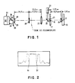
- FIG. 1 shows a measuring system for the lateral distance between an edge 11 of a first opaque object 13, for example a semiconductor wafer, and an edge 15 of a second object 17, for example a glass mask with a chrome pattern, in a schematic representation; the dimensions of the edges are exaggerated for illustration.
- the objects 13 and 17 are located in different planes, which are parallel to the projection lens 19 (for example a 32x / 0.60 guiding lens), which produces an image 21 of the edge 11 in the plane of the object 17 when the edges are caused by a light source 23 illuminated with coiiimized, monochromatic, spatially coherent light; a helium-neon laser (power 5 mw) can be used as the light source, for example, which is directed onto the edges via beam splitters 25.
- a helium-neon laser power 5 mw
- Edges 11 and 15 represent lines that are "substantially parallel”; this means the edges of a line, the edges of a square or a rectangle or the parallel tangent pieces of a circle or an ellipse.
- the lenses 27 (e.g. NIKKOR-P with f 105 mm) and 28 (e.g.
- Leitz 3.2x / 0.12) form the diffraction pattern 30, which is caused by interference between the light diffracted at edge 15 and the light of the image 21 from edge 11 arises, on a sensor 20 with a diode matrix 29: from;
- a suitable sensor is, for example, provided with the solid-line sampling circuits are arranged Model RL-256DA the Reticon Corporation, j at .dem 256 silicon photodiodes' with a spacing of 25 micrometers.
- the structure and mode of operation of the reticon scanner is described in US Pat. No. 3,957,376, to which reference is made here.
- Fig. 2 shows a drawing with the diffraction pattern as it is generated on an oscillograph screen using the system shown in Fig. 1.
- a computing and control device 31 supplies a start signal via line 38 and clock signals via line 36; it also receives the output signal of the diode matrix 29 via the video line 41.
- the structure and mode of operation of suitable control devices 31 for receiving and processing the diode matrix signals and the method for determining the distance between the edges is described in detail in US Pat. No. 3,957,376.
- the control devices include a computer 32, for example the IBM 360/30 model, with which the position of adjacent zeros in the diffraction pattern is determined.
- the lateral distance between the line edges results from the formula:
- the number of the specific minima is one. If the closest neighboring zeros of intensity are used, the number of the specific minima is two.
- the invention has many fields of application and, as described below, can be used to align objects with one another by determining the lateral distance of the respective line edges on each object and then displacing the objects against one another until the lateral distance reaches a value that indicates the alignment that has taken place; an example of this is the alignment of an exposure mask with respect to already existing patterns on a semiconductor wafer.
- the lateral distance of corresponding points on two objects can be determined in the same way, for example when comparing the patterns of different masks that are superimposed. of a mask set used to manufacture integrated circuits.
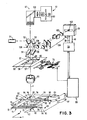
- Light source 51 provides collimated, monochromatic, spatially coherent light that falls on a beam splitter 52 and a mirror 53.
- a helium-cadmium laser with an output power of 15 mW can serve as the light source 51, for example a model from Spectraphysics.
- a Heliüm cadmium light source is namely compatible with the lens 60 of the projection exposure method corrected in blue and violet for the exposure of the photoresist. This eliminates the need for a correction lens if, on the one hand, the alignment is carried out with the aid of the laser light and, on the other hand, the exposure of the photoresist with the light source 61.
- Light source 61 comprises a mercury lamp 63, a condenser lens and a mirror arrangement 67.
- the light reflected by the beam splitter 52 and the mirror 53 passes through the beam splitters 54 and 55 and forms a light spot with a diameter of 0.16 mm for illuminating the alignment marks 57 and 57 'on mask 59 and the corresponding marks 67 and 67' on that with photoresist coated semiconductor wafer 69, which is arranged on an XY table 71.
- With closure shutters 106 the alignment marks on the left and right sides can be illuminated alternately.
- Mask 59 is contained in a frame 58, the notches 62 of which are brought into line with pin 64.
- Semiconductor wafer 69 is held in the correct position on table 71 by fingers 72; the fingers press the notch 73 in the semiconductor wafer against pin 74.
- a rotation system 75 for the mask permits its angular alignment with respect to the wafer 69 by rotation along an axis (not shown).
- the axis can be inside or on the side of the mask.
- the axis of rotation runs through the mask center on a line on which the center points of the two marks lie.
- the X-Y table 71 can be moved in the mutually orthogonal X and Y directions by the stepping motors 78, 79, 80 and 81.
- a pair of motors, one for coarse adjustment and one for fine adjustment of table 71, are provided for each direction.
- Table 71 has sensors 82 and 83 for the reference positions of the X and Y directions, respectively, in order to bring the center of the table into the reference position of the coordinates (0,0) which corresponds to the optical axis 1.
- the sensors 82 and 83 each include a pair of tandem optoelectronic image converters 94 and 95.
- tabs 96 which run in the same direction as the optoelectronic converters and whose width is selected such that they both do Interrupt light rays falling on the optoelectronic transducers at the same time and only when the table has the correct X or Y reference position.
- the laser interferometers 87 and 89 measure the movement and thus also the position of the table 71 in the X and Y directions; these interferometers are known in the art and comprise a pair of roof prisms 90 and 91 mounted on table 71 with the associated lasers 92 and 93.
- the laser interferometers include assigned counters 97, with which the table movement is recorded and sent to a system control unit 99, which in turn comprises, for example, a computer of the IBM Model 360/30 model.
- the control system 99 applies the motors 78, 79, 80 and 81 via the coarse and fine adjustment selector 101 to move the table over the desired distance in the X and Y directions.
- the arrangement of the interferometers and the motor control are known and are described in more detail, for example, in US Pat. No. 4,052,603, to which reference is made here.
- the X-Y table is shifted by the system controller 99 so that the alignment marks 67 and 67 'come into a position in which they are struck by the light beams used for the alignment.
- the alignment marks 67 and 67 ' comprise line edges which are etched into the semiconductor die in the usual way, at least one edge being provided in each mark for the two mutually orthogonal X and Y directions.
- Corresponding alignment marks 57 and 57 ' which also each have at least one line edge in the X and Y directions, are located on mask 59. There are several suitable configurations for the alignment marks.
- FIGS. 4a and 4b An example is shown in FIGS. 4a and 4b;
- FIG. 4a shows a directional marker pattern for a semiconductor wafer with pairs of parallel line edges in the X and Y directions.
- FIG. 4b shows a suitable directional marker with a pair of opaque squares, which consist, for example, of chromium.
- the diffraction patterns which are caused by corresponding line edges of the mask alignment marks 57 and 57 'and the image of the line edges of the marks 67 and 67' generated by the lens 60 in the plane of the mask 59, pass through the beam splitters 54 and 55, the lenses 102 (for example Nikkon photographic lens 55 mm), the mirror system 104 and the lens 105 (for example 3.2. Leitzmitoskop lens) for Diode matrix 103 of sensor 20; the latter can be, for example, a solid-state line scanner from Reticon Corporation (model RL-256-DA), in which silicon photodiodes 56 are arranged at intervals of 25 ⁇ .
- the diffraction patterns or the diode matrix can be rotated through 90 ° in a known manner in order to thus scan the patterns generated by the line edges in the X or Y direction.
- two rows of photo elements can also be provided in an orthogonal arrangement for the X and Y directions.
- the associated control devices 33 correspond to those described for the exemplary embodiment according to FIG. 1 with the exception that in this embodiment the computer is part of the control device 99 for the entire system. The distance between corresponding line edges is determined from the position of the minima in the diffraction pattern that is scanned by the diode matrix 103.
- the system controller 99 then controls the movement of the mask 59 and the semiconductor wafer 69 in order to set the distance between corresponding edge pairs of the alignment marks and thus align the patterns on the mask and the semiconductor wafer with respect to one another for the exposure process of the photoresist.
- the exposure takes place by closing the shutter 106 and opening the shutter 108; this causes light from mercury lamp 63 to fall onto the mask, which then falls with lens 60 onto the surface of the semiconductor wafer coated with photoresist and exposes the photoresist in accordance with the mask.
- the photoresist is then developed to produce the relief pattern from photoresist on the semiconductor wafer.
- the semiconductor wafer is provided with alignment marks 67 and 67 'as shown in FIG. 4a and the mask with alignment marks 57 and 57' as shown in FIG. 4b, then the mask 59 is placed in the mask holder and in accordance with FIG Semiconductor wafer 69 placed on the XY table.
- the mutual alignment procedure is then carried out as shown in FIGS. 5a, 5b and 5c.
- the XY table is moved out of the reference position (0,0) by a predetermined amount in order to bring the alignment marks of the semiconductor wafer into the area of the light beams of the alignment system; the mask is then set up so that the edge-to-edge distances have the nominal value for alignment.
- the table position in the X and Y directions is determined using the interferometer system.
- the left shutter 106 is set so that the illuminating beam is interrupted for the left alignment marks; the right shutter is opened, allowing the illuminating beam for the right marks to pass.
- the set of alignment marks on the right side is then set according to FIG. 5a.
- the dashed circle in FIG. 5a denotes the illumination spot, the images W2 and W4 of the edges of the semiconductor die are drawn in dashed lines, since they are covered by the opaque squares 2 and 3 of the mask alignment mark.
- the gap (X,) between the image W 1 of the edge on the semiconductor wafer and the edge M 1 of the mask is then determined from the position of the minima in the diffraction image.
- the gap (Y 1 ) between the image W 3 of the edge of the semiconductor wafer and the edge M 2 of the mask is determined from the minima of the diffraction image.
- the XY stage is then shifted to the right by a certain amount in the X direction and its position is determined with the laser interferometer; the alignment marks then have the position shown in FIG. 5b.
- the gap (Y z ) between the image W 4 of the edge on the semiconductor wafer and the edge M 2 of the mask is then determined on the basis of the minima of the diffraction image.
- the marks in the Y direction are aligned with each other if Y 1 and Y 2 are the same.
- the correct gap on each side of the edge M 2 is therefore equal to the measured values Y 1 plus Y 2 divided by two.
- the difference between the measured values of the gap and the correct gap is then known and the exact table position for the alignment in the Y direction at the right alignment mark can be calculated.
- the table is then moved down and to the left in the X and Y directions by a preselected amount, so that the alignment marks assume the position shown in FIG. 5c; the table position is measured again with the laser interferometer.
- the gap X 2 between the image W 2 of the edge on the semiconductor wafer and the edge M 2 of the mask is determined from the position of the minima in the diffraction image.
- the correct gap is found to be (measured values X 1 plus X z divided by two). It is assumed that the table has been returned to the original X position, as shown in Fig. 5a; if not, the values must be corrected according to the displacement in the X direction measured by the interferometer. The difference between the measured distances and the correct distance is then known, so that the correct table position for the X alignment of the alignment marks on the right-hand side can be calculated. The calculated values for the X and Y alignment for the right side, which are denoted by X R and R R , are thus known.
- the distances ⁇ at completion of alignment of marks 200 and the distance between the left and right marks is on the mask about 5 cm, as is the largest occurring misalignment in the axial direction (0), which must be corrected, 2.10- 4 wheel With this maximum possible error the Alignment in the axial direction as follows:
- the shutters 106 are then shifted so that the beam for the right marks is interrupted but the beam for the left marks passes.
- the difference ⁇ Y L between the distances in the Y direction of the Hken mark set is then determined by analyzing the diffraction patterns with the aid of the same steps with which the Y distances on the right side in accordance with the description above and FIGS. 5a and 5b were determined.
- the measured difference ⁇ Y L then corresponds to an angle ( ⁇ Y L ) °.
- ⁇ Y L angle
- the mask is turned around the angle rotated (d is the distance between the alignment marks), by which ⁇ Y L is brought to zero by half, ie to this also causes ⁇ Y ⁇ to go from zero to the value brought so that both the left and the right side by the amount are shifted in the same direction.
- the alignment is then carried out by moving the XY table by this amount in the Y direction.
- the distance between the lines of the alignment marks on the semiconductor wafer could first be measured with the aid of the analysis of diffraction figures, so that after the measurements in FIG and half of the measured distance between the alignment lines on the semiconductor wafer.
- the axis for the mask rotation need not run through the center line between the alignment marks; Knowing their position is sufficient, since the alignment algorithm can then be modified according to the position of the fulcrum. It is also not necessary for continuous measurement to be carried out between the left and right alignment marks. Each of the items can be moved for alignment. If lens 60 provides a reduction in the size of the image, positional errors of the mask with its larger pattern are less important, so that when the mask is shifted for precise alignment, less accurate measurements are required than when the semiconductor wafer is shifted.
- the invention can be used not only for the mutual alignment of objects, but also for determining the distance of line edges on two objects.
- the overlap of patterns on two objects can be measured by measuring the overlaps at different points on the pattern. This is necessary, for example, if a series of masks for different manufacturing stages of integrated circuits are generated with a step camera that images individual sections side by side. If the position of the individual repeated pattern sections differs from mask to mask, errors occur in the alignment of the patterns within the masks and the patterns on the semiconductor wafer which exceed the permissible tolerances for the production of integrated circuits, even when the masks are precisely aligned lie. Sets of masks can therefore be checked for the prescribed overlap with the aid of the invention to ensure that they can be used to produce integrated circuits with good yield.
- the image of the pattern on the semiconductor wafer at the location of the mask can be generated using optical systems that use specular or refractive elements. If two transparent objects, such as masks, are present, the measurement can also take place behind the second object with the diffraction image which is formed by the image of the edge lying on the first object in the plane of the second object.
Claims (10)
Applications Claiming Priority (2)
| Application Number | Priority Date | Filing Date | Title |
|---|---|---|---|
| US05/865,807 US4172664A (en) | 1977-12-30 | 1977-12-30 | High precision pattern registration and overlay measurement system and process |
| US865807 | 1977-12-30 |
Publications (3)
| Publication Number | Publication Date |
|---|---|
| EP0002668A2 EP0002668A2 (fr) | 1979-07-11 |
| EP0002668A3 EP0002668A3 (en) | 1979-07-25 |
| EP0002668B1 true EP0002668B1 (fr) | 1982-04-28 |
Family
ID=25346276
Family Applications (1)
| Application Number | Title | Priority Date | Filing Date |
|---|---|---|---|
| EP78101459A Expired EP0002668B1 (fr) | 1977-12-30 | 1978-11-27 | Dispositif de mesure optique de la distance |
Country Status (5)
| Country | Link |
|---|---|
| US (1) | US4172664A (fr) |
| EP (1) | EP0002668B1 (fr) |
| JP (1) | JPS5495267A (fr) |
| CA (1) | CA1104338A (fr) |
| DE (1) | DE2861769D1 (fr) |
Families Citing this family (22)
| Publication number | Priority date | Publication date | Assignee | Title |
|---|---|---|---|---|
| FR2472209A1 (fr) * | 1979-12-18 | 1981-06-26 | Thomson Csf | Systeme optique d'alignement automatique de deux motifs comportant des reperes s'alignement du type reseaux, notamment en photo-repetition directe sur silicium |
| DE3071858D1 (en) * | 1980-07-31 | 1987-01-22 | Ibm | Method and device for optical distance measurement |
| JPS58193547A (ja) * | 1982-05-07 | 1983-11-11 | Hitachi Ltd | 縮小投影露光装置 |
| JPS5998525A (ja) * | 1982-11-26 | 1984-06-06 | Canon Inc | 分割焼付け装置のアライメント方法 |
| JPH0619280B2 (ja) * | 1983-09-24 | 1994-03-16 | 名古屋大学長 | 光学式自動位置決め装置 |
| DE3336901A1 (de) * | 1983-10-11 | 1985-04-18 | Deutsche Itt Industries Gmbh, 7800 Freiburg | Maskenmarkierung und substratmarkierung fuer ein verfahren zum justieren einer eine maskenmarkierung enthaltenden photomaske auf einer substratmarkierung |
| US4679942A (en) * | 1984-02-24 | 1987-07-14 | Nippon Kogaku K. K. | Method of aligning a semiconductor substrate and a photomask |
| US4703434A (en) * | 1984-04-24 | 1987-10-27 | The Perkin-Elmer Corporation | Apparatus for measuring overlay error |
| US7115858B1 (en) | 2000-09-25 | 2006-10-03 | Nanometrics Incorporated | Apparatus and method for the measurement of diffracting structures |
| US6819426B2 (en) * | 2001-02-12 | 2004-11-16 | Therma-Wave, Inc. | Overlay alignment metrology using diffraction gratings |
| US6898537B1 (en) | 2001-04-27 | 2005-05-24 | Nanometrics Incorporated | Measurement of diffracting structures using one-half of the non-zero diffracted orders |
| US6713753B1 (en) | 2001-07-03 | 2004-03-30 | Nanometrics Incorporated | Combination of normal and oblique incidence polarimetry for the characterization of gratings |
| US7061615B1 (en) | 2001-09-20 | 2006-06-13 | Nanometrics Incorporated | Spectroscopically measured overlay target |
| KR100385066B1 (ko) * | 2001-10-16 | 2003-05-23 | 삼성전자주식회사 | 레이저 스캐닝 유니트 |
| US6982793B1 (en) | 2002-04-04 | 2006-01-03 | Nanometrics Incorporated | Method and apparatus for using an alignment target with designed in offset |
| US6949462B1 (en) | 2002-04-04 | 2005-09-27 | Nanometrics Incorporated | Measuring an alignment target with multiple polarization states |
| US6992764B1 (en) | 2002-09-30 | 2006-01-31 | Nanometrics Incorporated | Measuring an alignment target with a single polarization state |
| US7582538B2 (en) * | 2005-04-06 | 2009-09-01 | Taiwan Semiconductor Manufacturing Company, Ltd. | Method of overlay measurement for alignment of patterns in semiconductor manufacturing |
| US7432605B2 (en) * | 2006-09-21 | 2008-10-07 | Macronix International Co., Ltd. | Overlay mark, method for forming the same and application thereof |
| US7990528B2 (en) * | 2009-09-29 | 2011-08-02 | Xerox Corporation | High resolution linear image sensing using multi-row low resolution image sensor |
| PL224191B1 (pl) | 2012-05-25 | 2016-11-30 | Polska Spółka Inżynierska Digilab Spółka Z Ograniczoną | Sposób wyznaczania wartości wymiaru liniowego obiektu oraz optyczne urządzenie do wyznaczania wymiaru liniowego obiektu |
| US10822890B2 (en) | 2018-06-15 | 2020-11-03 | Rus-Tec Engineering, Ltd. | Pipe handling apparatus |
Family Cites Families (9)
| Publication number | Priority date | Publication date | Assignee | Title |
|---|---|---|---|---|
| GB1231431A (fr) * | 1967-06-24 | 1971-05-12 | ||
| US3507597A (en) * | 1967-09-26 | 1970-04-21 | Bausch & Lomb | Lens axial alignment method and apparatus |
| US3797939A (en) * | 1968-08-09 | 1974-03-19 | T Pryor | Diffractographic measurement of profile |
| JPS5117297B1 (fr) * | 1971-03-11 | 1976-06-01 | ||
| US3796497A (en) * | 1971-12-01 | 1974-03-12 | Ibm | Optical alignment method and apparatus |
| US3883249A (en) * | 1972-05-15 | 1975-05-13 | Timothy R Pryor | Z-factor and other diffractographic displacement and profile sensors |
| US3957376A (en) * | 1974-01-25 | 1976-05-18 | International Business Machines Corporation | Measuring method and system using a diffraction pattern |
| US4037969A (en) * | 1976-04-02 | 1977-07-26 | Bell Telephone Laboratories, Incorporated | Zone plate alignment marks |
| NL7606548A (nl) * | 1976-06-17 | 1977-12-20 | Philips Nv | Werkwijze en inrichting voor het uitrichten van een i.c.-patroon ten opzichte van een halfgelei- dend substraat. |
-
1977
- 1977-12-30 US US05/865,807 patent/US4172664A/en not_active Expired - Lifetime
-
1978
- 1978-09-29 CA CA312,413A patent/CA1104338A/fr not_active Expired
- 1978-11-24 JP JP14436878A patent/JPS5495267A/ja active Granted
- 1978-11-27 EP EP78101459A patent/EP0002668B1/fr not_active Expired
- 1978-11-27 DE DE7878101459T patent/DE2861769D1/de not_active Expired
Also Published As
| Publication number | Publication date |
|---|---|
| DE2861769D1 (en) | 1982-06-09 |
| JPS5495267A (en) | 1979-07-27 |
| EP0002668A2 (fr) | 1979-07-11 |
| EP0002668A3 (en) | 1979-07-25 |
| CA1104338A (fr) | 1981-07-07 |
| US4172664A (en) | 1979-10-30 |
| JPS6351241B2 (fr) | 1988-10-13 |
Similar Documents
| Publication | Publication Date | Title |
|---|---|---|
| EP0002668B1 (fr) | Dispositif de mesure optique de la distance | |
| DE3104007C2 (fr) | ||
| DE3512064C2 (de) | Gerät zur Messung von Überdeckungsfehlern | |
| DE69133544T2 (de) | Vorrichtung zur Projektion eines Maskenmusters auf ein Substrat | |
| DE69631260T2 (de) | Abtastbelichtungsapparat, Belichtungsverfahren unter Verwendung desselben und Verfahren zur Herstellung der Vorrichtung | |
| DE2557675C2 (de) | Verfahren zum Ausrichten von mit zwei Markierungen von bekanntem Abstand versehenen planaren Werkstücken | |
| DE19837037B4 (de) | Retikel, Belichtungsverfahren, Belichtungsgerät und Halbleitervorrichtung | |
| DE3114682C2 (fr) | ||
| DE69827608T2 (de) | Ausrichtungsvorrichtung und lithographischer apparat mit einer solchen vorrichtung | |
| DE60113153T2 (de) | Verfahren zur Messung der Ausrichtung eines Substrats bezüglich einer Referenz-Ausrichtmarke | |
| DE3643578C2 (de) | Projektionsbelichtungsvorrichtung und Verfahren für deren Betrieb | |
| DE69839069T2 (de) | Wiederholte projektion eines maskenmusters unter verwendung einer zeitsparenden höhenmessung | |
| DE69738335T2 (de) | Verfahren zur Detektion einer Oberflächenlage und Abtastbelichtungsverfahren unter Verwendung derselbe | |
| DE3213338C2 (de) | Verfahren und Vorrichtung zum Justieren eines Substrates, insbesondere eines Halbleiterwafers | |
| DE3342719C2 (de) | Positionierungseinrichung in einem Projektionsbelichter | |
| DE1919991B2 (de) | Anordnung zur automatischen ausrichtung von zwei aufeinander einzujustierenden objekten | |
| DE2900921C2 (de) | Verfahren zum Projektionskopieren von Masken auf ein Werkstück | |
| DE2260229C3 (fr) | ||
| DE10225423A1 (de) | Fotomaske zur Fokusüberwachung, Verfahren zur Fokusüberwachung, Einheit zur Fokusüberwachung und Herstellungsverfahren für eine derartige Einheit | |
| DE2817400A1 (de) | Verfahren zum ausrichten eines halbleiterplaettchens und nach diesem verfahren arbeitender photowiederholer | |
| DE69838564T2 (de) | Detektor mit mehreren Öffnungen für die Photolithographie | |
| DE2948646C2 (de) | Projektionskopiervorrichtung | |
| DE3942678C2 (de) | Belichtungssystem mit Ausrichtsystem | |
| EP0135673B1 (fr) | Procédé et dispositif pour déterminer une coordonnée sur la surface d'un corps solide | |
| DE3343181C2 (fr) |
Legal Events
| Date | Code | Title | Description |
|---|---|---|---|
| PUAI | Public reference made under article 153(3) epc to a published international application that has entered the european phase |
Free format text: ORIGINAL CODE: 0009012 |
|
| PUAL | Search report despatched |
Free format text: ORIGINAL CODE: 0009013 |
|
| AK | Designated contracting states |
Designated state(s): DE FR GB |
|
| AK | Designated contracting states |
Designated state(s): DE FR GB |
|
| 17P | Request for examination filed | ||
| GRAA | (expected) grant |
Free format text: ORIGINAL CODE: 0009210 |
|
| AK | Designated contracting states |
Designated state(s): DE FR GB |
|
| REF | Corresponds to: |
Ref document number: 2861769 Country of ref document: DE Date of ref document: 19820609 |
|
| PGFP | Annual fee paid to national office [announced via postgrant information from national office to epo] |
Ref country code: DE Payment date: 19921121 Year of fee payment: 15 |
|
| PGFP | Annual fee paid to national office [announced via postgrant information from national office to epo] |
Ref country code: FR Payment date: 19931103 Year of fee payment: 16 |
|
| PG25 | Lapsed in a contracting state [announced via postgrant information from national office to epo] |
Ref country code: DE Effective date: 19940802 |
|
| PGFP | Annual fee paid to national office [announced via postgrant information from national office to epo] |
Ref country code: GB Payment date: 19941013 Year of fee payment: 17 |
|
| PG25 | Lapsed in a contracting state [announced via postgrant information from national office to epo] |
Ref country code: FR Effective date: 19950731 |
|
| REG | Reference to a national code |
Ref country code: FR Ref legal event code: ST |
|
| PG25 | Lapsed in a contracting state [announced via postgrant information from national office to epo] |
Ref country code: GB Effective date: 19951127 |
|
| GBPC | Gb: european patent ceased through non-payment of renewal fee |
Effective date: 19951127 |
|
| PLBE | No opposition filed within time limit |
Free format text: ORIGINAL CODE: 0009261 |
|
| STAA | Information on the status of an ep patent application or granted ep patent |
Free format text: STATUS: NO OPPOSITION FILED WITHIN TIME LIMIT |