EP0001952B1 - Diode émettrice et réceptrice de rayons lumineux de même longueur d'onde prédéterminée - Google Patents
Diode émettrice et réceptrice de rayons lumineux de même longueur d'onde prédéterminée Download PDFInfo
- Publication number
- EP0001952B1 EP0001952B1 EP78400155A EP78400155A EP0001952B1 EP 0001952 B1 EP0001952 B1 EP 0001952B1 EP 78400155 A EP78400155 A EP 78400155A EP 78400155 A EP78400155 A EP 78400155A EP 0001952 B1 EP0001952 B1 EP 0001952B1
- Authority
- EP
- European Patent Office
- Prior art keywords
- layer
- diode
- accordance
- layers
- type
- Prior art date
- Legal status (The legal status is an assumption and is not a legal conclusion. Google has not performed a legal analysis and makes no representation as to the accuracy of the status listed.)
- Expired
Links
- 239000000758 substrate Substances 0.000 claims description 8
- 229910045601 alloy Inorganic materials 0.000 claims description 4
- 239000000956 alloy Substances 0.000 claims description 4
- 229910052751 metal Inorganic materials 0.000 claims description 2
- 239000002184 metal Substances 0.000 claims description 2
- 239000004065 semiconductor Substances 0.000 claims description 2
- 230000017525 heat dissipation Effects 0.000 claims 1
- 229910002059 quaternary alloy Inorganic materials 0.000 claims 1
- 229910002058 ternary alloy Inorganic materials 0.000 claims 1
- 230000010287 polarization Effects 0.000 description 5
- 230000005855 radiation Effects 0.000 description 4
- 230000004888 barrier function Effects 0.000 description 3
- JBRZTFJDHDCESZ-UHFFFAOYSA-N AsGa Chemical compound [As]#[Ga] JBRZTFJDHDCESZ-UHFFFAOYSA-N 0.000 description 2
- 229910001218 Gallium arsenide Inorganic materials 0.000 description 2
- 230000005540 biological transmission Effects 0.000 description 2
- 239000000969 carrier Substances 0.000 description 2
- 230000008094 contradictory effect Effects 0.000 description 2
- 239000000203 mixture Substances 0.000 description 2
- 238000005036 potential barrier Methods 0.000 description 2
- 241001080024 Telles Species 0.000 description 1
- 230000003667 anti-reflective effect Effects 0.000 description 1
- 239000012141 concentrate Substances 0.000 description 1
- 239000013078 crystal Substances 0.000 description 1
- 230000008021 deposition Effects 0.000 description 1
- 238000009792 diffusion process Methods 0.000 description 1
- 238000005401 electroluminescence Methods 0.000 description 1
- 239000000835 fiber Substances 0.000 description 1
- 239000000463 material Substances 0.000 description 1
- 239000013307 optical fiber Substances 0.000 description 1
- 230000035945 sensitivity Effects 0.000 description 1
- 239000000126 substance Substances 0.000 description 1
Images


Classifications
-
- H—ELECTRICITY
- H04—ELECTRIC COMMUNICATION TECHNIQUE
- H04B—TRANSMISSION
- H04B10/00—Transmission systems employing electromagnetic waves other than radio-waves, e.g. infrared, visible or ultraviolet light, or employing corpuscular radiation, e.g. quantum communication
- H04B10/40—Transceivers
- H04B10/43—Transceivers using a single component as both light source and receiver, e.g. using a photoemitter as a photoreceiver
-
- H—ELECTRICITY
- H01—ELECTRIC ELEMENTS
- H01L—SEMICONDUCTOR DEVICES NOT COVERED BY CLASS H10
- H01L31/00—Semiconductor devices sensitive to infrared radiation, light, electromagnetic radiation of shorter wavelength or corpuscular radiation and specially adapted either for the conversion of the energy of such radiation into electrical energy or for the control of electrical energy by such radiation; Processes or apparatus specially adapted for the manufacture or treatment thereof or of parts thereof; Details thereof
- H01L31/08—Semiconductor devices sensitive to infrared radiation, light, electromagnetic radiation of shorter wavelength or corpuscular radiation and specially adapted either for the conversion of the energy of such radiation into electrical energy or for the control of electrical energy by such radiation; Processes or apparatus specially adapted for the manufacture or treatment thereof or of parts thereof; Details thereof in which radiation controls flow of current through the device, e.g. photoresistors
- H01L31/10—Semiconductor devices sensitive to infrared radiation, light, electromagnetic radiation of shorter wavelength or corpuscular radiation and specially adapted either for the conversion of the energy of such radiation into electrical energy or for the control of electrical energy by such radiation; Processes or apparatus specially adapted for the manufacture or treatment thereof or of parts thereof; Details thereof in which radiation controls flow of current through the device, e.g. photoresistors characterised by potential barriers, e.g. phototransistors
- H01L31/101—Devices sensitive to infrared, visible or ultraviolet radiation
- H01L31/102—Devices sensitive to infrared, visible or ultraviolet radiation characterised by only one potential barrier
- H01L31/109—Devices sensitive to infrared, visible or ultraviolet radiation characterised by only one potential barrier the potential barrier being of the PN heterojunction type
-
- H—ELECTRICITY
- H01—ELECTRIC ELEMENTS
- H01L—SEMICONDUCTOR DEVICES NOT COVERED BY CLASS H10
- H01L31/00—Semiconductor devices sensitive to infrared radiation, light, electromagnetic radiation of shorter wavelength or corpuscular radiation and specially adapted either for the conversion of the energy of such radiation into electrical energy or for the control of electrical energy by such radiation; Processes or apparatus specially adapted for the manufacture or treatment thereof or of parts thereof; Details thereof
- H01L31/12—Semiconductor devices sensitive to infrared radiation, light, electromagnetic radiation of shorter wavelength or corpuscular radiation and specially adapted either for the conversion of the energy of such radiation into electrical energy or for the control of electrical energy by such radiation; Processes or apparatus specially adapted for the manufacture or treatment thereof or of parts thereof; Details thereof structurally associated with, e.g. formed in or on a common substrate with, one or more electric light sources, e.g. electroluminescent light sources, and electrically or optically coupled thereto
- H01L31/125—Composite devices with photosensitive elements and electroluminescent elements within one single body
-
- H—ELECTRICITY
- H01—ELECTRIC ELEMENTS
- H01L—SEMICONDUCTOR DEVICES NOT COVERED BY CLASS H10
- H01L33/00—Semiconductor devices having potential barriers specially adapted for light emission; Processes or apparatus specially adapted for the manufacture or treatment thereof or of parts thereof; Details thereof
- H01L33/0004—Devices characterised by their operation
- H01L33/002—Devices characterised by their operation having heterojunctions or graded gap
- H01L33/0025—Devices characterised by their operation having heterojunctions or graded gap comprising only AIIIBV compounds
Definitions
- the present invention relates to a diode emitting and receiving light rays of the same predetermined wavelength.
- the emissive zone must have a low thickness so as not to absorb the photons which it generates. It must be heavily doped to have a sufficiently short response time.
- the receiving zone must have a thickness large enough to absorb the photons, and consequently create an electric current and have a weak enough doping to be at least partly in charge of space when the reverse bias voltage is applied.
- these two layers must be prohibited bands of different width.
- the emitting and receiving diode according to the invention is mainly characterized by the superposition of a first emitting layer of a first type of conductivity and of a second receiving layer of a second type of conductivity opposite to the first, the bandwidth the prohibited layer is less than that of the transmitting layer, a third layer of prohibited bandwidth greater than those of the first and second layers being interposed therebetween.
- the substrate and the layer 2 are made of Gallium Arsenide GaAs, the layers 1, 3 and 4 of alloy Ca 1-x , Al x , As.
- Layer 4 has a very large forbidden bandwidth, of the order of 1.8 eV, a thickness of the order of 1 ⁇ m, layer 1, a smaller forbidden bandwidth of the order of 1 , 5 eV, layer 3 with a thickness of around 0.3 ⁇ m has a much larger band gap of 1.8 eV, for example, layer 2 with thickness of the order of 2 ⁇ m at smallest prohibited bandwidth, 1.4 eV and finally the substrate, a prohibited bandwidth of the order of 1.4 eV, and a thickness of 10 to 200 ⁇ m.
- Figure 2 shows when there is no external polarization, the energy levels Ec and Ev of the conduction bands and valence bands of the various regions.
- zone 3 inserted between zones 1 and 2 defines a potential barrier with zone 1.
- the energy levels occupied in the valence bands of regions 1 and 4 correspond to P-type doping.
- the energy levels occupied in the conduction band of zones 3 and 2 correspond to N-type doping. These energy levels being occupied only on either side of the junction, no electric current will not pass.
- zone 1 there are in zone 1, both in the valence and conduction bands, respectively holes and excess electrons. By recombining, these holes and these electrons give rise to the phenomenon of electroluminescence by the creation of photons.
- the holes cannot cross the barrier formed by the valence band in zone 3, and the electrons the barrier formed by the conduction band in zone 4.
- the radiation frequency is proportional to the width of the band prohibited in zone 1.
- the thickness of zone 1, of the order of 1 ⁇ m and its doping of the order of 10 11 at / cm 3 are chosen in an optimal manner, so that the yield in photo- emission and modulation speed of the diode are as high as possible.
- zone 4 is connected to the pole - of a polarization source, the substrate to its pole +. It follows that the potential barriers are accentuated in the vicinity of the junction, and that zones 3 and especially 2 are in charge of space.
- This zone can therefore have a sufficient thickness, 2 ⁇ m for example to absorb the photons, and a weak doping 10 15 at / cm 3 for example, to be easily loaded with space.
- the role of zone 3 is to form the barriers necessary to separate the two functions: transmission and reception. Its thickness 0.3 ⁇ m for example may be small. It is essentially its forbidden bandwidth which must be large and its doping sufficiently low for the space charge to extend in layer 2.
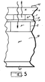
- FIG. 5 represents a diode according to the invention, in which all the types of conductivity are reversed. Furthermore, the design is identical.
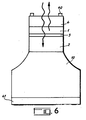
- FIG. 6 represents an exemplary embodiment in the form of a "mesa", the zone 4 exposed to light radiation comprises an annular contact 40.
- the substrate 10 comprises on its free surface a contact 41.
- FIG. 7 Another embodiment is shown in Figure 7.
- the substrate 10 is transparent and its free face is exposed to radiation.
- the arrangement of layers 1, 2, 3 and 4 is reversed compared to the previous figures.
- Layer 2 is welded onto a metal support 42, which serves both as a heat radiator and as a contact: this arrangement promotes the evacuation of heat.
- the diode is of the so-called “mesa diode” welded upside down "type.
- an N-type layer 5, with a small prohibited band, is interposed between zones 2 and 3, it can serve as an avalanche multiplication layer of the electrons generated in layer 2.
- the avalanche phenomenon could occur in layer 3. But in case this doping becomes too high, it can be difficult to put layers 2 and 3 in charge of space.
- the presence of layer 5 in Figure 8 solves this problem.
- the prohibited bandwidth is an increasing function of the value x.
- the layers 1, 2, 3 and 4 will for example have x values respectively of 0.07, for the layer 1, close to 0 for the layer 2, of 0.3 for the layers 3 and 4.
- an anti-reflective treatment that is to say by the deposition on the free surface of the diode (zone 4 or substrate) of a dielectric layer of quarter-wave thickness of known type. , a sensitivity close to 100 A per watt.
- the response time to reception can be short since all carriers are created in the area in charge of space; therefore no natural diffusion process takes place.
- the transit time of the carriers created in the area in charge of space, with a thickness of the order of 2 .mu.m can be less than 100 ps.
- materials other than alloys of the Ga, AI, As type can be used, for example structures based on ternary or quaternary mixtures taken from groups 3 and 5 of the Mendeleef classification.
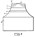
- FIG. 9 represents a structure combining the solutions described in this application and in the French patent application filed on October 18, 1977 under No. 77 31 274 by the applicant and to which the European patent application filed under the number 78400120.8 corresponds. and published under the number 1728.
- annular zone 45 made insulating is provided which makes it possible to concentrate the emission of the current lines in the central part of the diode.
- the invention can also be extended to semiconductor laser structures, FIG. 10.
- the assembly is a single crystal cleaved on two faces.
- Fiber 100 is coupled as shown, layers 2 and 1 receiving and emitting light radiation through the wafer.
Landscapes
- Engineering & Computer Science (AREA)
- Physics & Mathematics (AREA)
- Electromagnetism (AREA)
- Computer Hardware Design (AREA)
- Microelectronics & Electronic Packaging (AREA)
- Power Engineering (AREA)
- Condensed Matter Physics & Semiconductors (AREA)
- General Physics & Mathematics (AREA)
- Chemical & Material Sciences (AREA)
- Composite Materials (AREA)
- Computer Networks & Wireless Communication (AREA)
- Signal Processing (AREA)
- Manufacturing & Machinery (AREA)
- Light Receiving Elements (AREA)
- Led Devices (AREA)
- Led Device Packages (AREA)
- Photo Coupler, Interrupter, Optical-To-Optical Conversion Devices (AREA)
- Optical Communication System (AREA)
Applications Claiming Priority (2)
| Application Number | Priority Date | Filing Date | Title |
|---|---|---|---|
| FR7733354A FR2408222A1 (fr) | 1977-11-07 | 1977-11-07 | Diode emettrice et receptrice de rayons lumineux de meme longueur d'onde predeterminee et dispositif de telecommunication optique utilisant une telle diode |
| FR7733354 | 1977-11-07 |
Publications (3)
| Publication Number | Publication Date |
|---|---|
| EP0001952A2 EP0001952A2 (fr) | 1979-05-16 |
| EP0001952A3 EP0001952A3 (en) | 1979-05-30 |
| EP0001952B1 true EP0001952B1 (fr) | 1980-12-10 |
Family
ID=9197316
Family Applications (1)
| Application Number | Title | Priority Date | Filing Date |
|---|---|---|---|
| EP78400155A Expired EP0001952B1 (fr) | 1977-11-07 | 1978-10-27 | Diode émettrice et réceptrice de rayons lumineux de même longueur d'onde prédéterminée |
Country Status (6)
| Country | Link |
|---|---|
| US (1) | US4217597A (ja) |
| EP (1) | EP0001952B1 (ja) |
| JP (1) | JPS5475288A (ja) |
| CA (1) | CA1121490A (ja) |
| DE (1) | DE2860308D1 (ja) |
| FR (1) | FR2408222A1 (ja) |
Families Citing this family (4)
| Publication number | Priority date | Publication date | Assignee | Title |
|---|---|---|---|---|
| DE3046140A1 (de) * | 1980-12-06 | 1982-07-15 | Licentia Patent-Verwaltungs-Gmbh, 6000 Frankfurt | "signaluebertragungsverfahren, ein halbleiter-bauelement sowie ein elektro-optisches bauelement zur durchfuehrung des verfahrens" |
| EP0096509A3 (en) * | 1982-06-09 | 1986-02-26 | National Research Development Corporation | Electroluminescent devices |
| JPS60230329A (ja) * | 1984-04-27 | 1985-11-15 | オプテツクス株式会社 | 赤外線式光電スイツチ |
| FR2724769B1 (fr) * | 1994-09-16 | 1996-12-06 | Thomson Csf | Procede de realisation de diodes laser a emission surfacique |
Family Cites Families (6)
| Publication number | Priority date | Publication date | Assignee | Title |
|---|---|---|---|---|
| FR2175571B1 (ja) * | 1972-03-14 | 1978-08-25 | Radiotechnique Compelec | |
| US3946334A (en) * | 1973-11-14 | 1976-03-23 | Nippon Electric Company, Limited | Injection semiconductor laser device |
| FR2273371B1 (ja) * | 1974-05-28 | 1978-03-31 | Thomson Csf | |
| FR2275078A1 (fr) * | 1974-06-14 | 1976-01-09 | Thomson Csf | Systeme de telecommunications optiques bidirectionnelles |
| JPS51146196A (en) * | 1975-06-11 | 1976-12-15 | Hitachi Ltd | Diode laser |
| JPS53116792A (en) * | 1977-03-23 | 1978-10-12 | Toshiba Corp | Semiconductor light emitting-photo detecting composite device |
-
1977
- 1977-11-07 FR FR7733354A patent/FR2408222A1/fr active Granted
-
1978
- 1978-10-27 EP EP78400155A patent/EP0001952B1/fr not_active Expired
- 1978-10-27 DE DE7878400155T patent/DE2860308D1/de not_active Expired
- 1978-10-31 CA CA000315358A patent/CA1121490A/en not_active Expired
- 1978-11-02 US US05/957,196 patent/US4217597A/en not_active Expired - Lifetime
- 1978-11-07 JP JP13720678A patent/JPS5475288A/ja active Granted
Also Published As
| Publication number | Publication date |
|---|---|
| FR2408222B1 (ja) | 1980-04-25 |
| CA1121490A (en) | 1982-04-06 |
| FR2408222A1 (fr) | 1979-06-01 |
| EP0001952A3 (en) | 1979-05-30 |
| DE2860308D1 (en) | 1981-02-19 |
| JPS5475288A (en) | 1979-06-15 |
| JPS6244714B2 (ja) | 1987-09-22 |
| US4217597A (en) | 1980-08-12 |
| EP0001952A2 (fr) | 1979-05-16 |
Similar Documents
| Publication | Publication Date | Title |
|---|---|---|
| US4202000A (en) | Diode capable of alternately functioning as an emitter and detector of light of the same wavelength | |
| EP0545808B1 (fr) | Dispositif optoélectronique à très faible résistance série | |
| FR2538171A1 (fr) | Diode electroluminescente a emission de surface | |
| EP3084843B1 (fr) | Elément de détection quantique à faible bruit et procédé de fabrication d'un tel élément de photodétection | |
| EP0001728B1 (fr) | Diode émettrice et réceptrice de lumière notamment pour télécommunications optiques | |
| JP2004104085A (ja) | アバランシェフォトトランジスタ | |
| FR2757684A1 (fr) | Detecteur infrarouge a structure quantique, non refroidie | |
| EP0001952B1 (fr) | Diode émettrice et réceptrice de rayons lumineux de même longueur d'onde prédéterminée | |
| EP0069608B1 (fr) | Laser à semiconductor à courte longeur d'onde | |
| JP4861388B2 (ja) | アバランシェホトダイオード | |
| JPS5984589A (ja) | アバランシフオトダイオード | |
| EP0454566B1 (fr) | Laser compact à semi-conducteur du type à pompage électronique | |
| JP2001267620A (ja) | 半導体受光素子 | |
| JPH038117B2 (ja) | ||
| EP0082787B1 (fr) | Photodiode à zones d'absorption et d'avalanche séparées | |
| EP0664588A1 (fr) | Structure semiconductrice à réseau de diffraction virtuel | |
| CA1182200A (en) | High sensitivity photon feedback photodetectors | |
| EP0308335A2 (en) | InGaAs/InP type PIN photodiodes | |
| JPH06350134A (ja) | InAsSb発光ダイオード及びその使用方法 | |
| FR2509910A1 (fr) | Composant optoelectronique dont la structure semiconductrice comporte deux parties respectivement emettrice et receptrice, et dispositif de regulation d'une diode electroluminescente | |
| RU2261501C2 (ru) | Полупроводниковый источник инфракрасного излучения | |
| US20040017600A1 (en) | Electroabsorption modulator, modulator laser device and method for producing an electroabsorption modulator | |
| JPH051629B2 (ja) | ||
| FR2485823A1 (fr) | Laser semi-conducteur | |
| FR2721439A1 (fr) | Eléments semi-conducteurs optiques et procédés de fabrication de ceux-ci. |
Legal Events
| Date | Code | Title | Description |
|---|---|---|---|
| PUAI | Public reference made under article 153(3) epc to a published international application that has entered the european phase |
Free format text: ORIGINAL CODE: 0009012 |
|
| PUAL | Search report despatched |
Free format text: ORIGINAL CODE: 0009013 |
|
| AK | Designated contracting states |
Designated state(s): DE GB NL |
|
| AK | Designated contracting states |
Designated state(s): DE GB NL |
|
| 17P | Request for examination filed | ||
| GRAA | (expected) grant |
Free format text: ORIGINAL CODE: 0009210 |
|
| AK | Designated contracting states |
Designated state(s): DE GB NL |
|
| REF | Corresponds to: |
Ref document number: 2860308 Country of ref document: DE Date of ref document: 19810219 |
|
| PGFP | Annual fee paid to national office [announced via postgrant information from national office to epo] |
Ref country code: DE Payment date: 19920917 Year of fee payment: 15 |
|
| PGFP | Annual fee paid to national office [announced via postgrant information from national office to epo] |
Ref country code: GB Payment date: 19920918 Year of fee payment: 15 |
|
| PGFP | Annual fee paid to national office [announced via postgrant information from national office to epo] |
Ref country code: NL Payment date: 19921031 Year of fee payment: 15 |
|
| PG25 | Lapsed in a contracting state [announced via postgrant information from national office to epo] |
Ref country code: GB Effective date: 19931027 |
|
| PG25 | Lapsed in a contracting state [announced via postgrant information from national office to epo] |
Ref country code: NL Effective date: 19940501 |
|
| NLV4 | Nl: lapsed or anulled due to non-payment of the annual fee | ||
| GBPC | Gb: european patent ceased through non-payment of renewal fee |
Effective date: 19931027 |
|
| PG25 | Lapsed in a contracting state [announced via postgrant information from national office to epo] |
Ref country code: DE Effective date: 19940802 |
|
| PLBE | No opposition filed within time limit |
Free format text: ORIGINAL CODE: 0009261 |
|
| STAA | Information on the status of an ep patent application or granted ep patent |
Free format text: STATUS: NO OPPOSITION FILED WITHIN TIME LIMIT |