EP0000613B1 - Kathodenstrahlröhre-Speichervorrichtung mit Elektrolumineszenz-Bildschirm - Google Patents
Kathodenstrahlröhre-Speichervorrichtung mit Elektrolumineszenz-Bildschirm Download PDFInfo
- Publication number
- EP0000613B1 EP0000613B1 EP78300019A EP78300019A EP0000613B1 EP 0000613 B1 EP0000613 B1 EP 0000613B1 EP 78300019 A EP78300019 A EP 78300019A EP 78300019 A EP78300019 A EP 78300019A EP 0000613 B1 EP0000613 B1 EP 0000613B1
- Authority
- EP
- European Patent Office
- Prior art keywords
- layer
- electroluminescent
- storage device
- cathode ray
- ray tube
- Prior art date
- Legal status (The legal status is an assumption and is not a legal conclusion. Google has not performed a legal analysis and makes no representation as to the accuracy of the status listed.)
- Expired
Links
- 239000000463 material Substances 0.000 claims description 50
- 238000010894 electron beam technology Methods 0.000 claims description 30
- 230000005855 radiation Effects 0.000 claims description 17
- 239000004020 conductor Substances 0.000 claims description 10
- 239000011810 insulating material Substances 0.000 claims description 5
- 230000004044 response Effects 0.000 claims description 4
- 230000001747 exhibiting effect Effects 0.000 claims description 3
- 230000006335 response to radiation Effects 0.000 claims description 2
- 230000000007 visual effect Effects 0.000 claims description 2
- 230000001939 inductive effect Effects 0.000 claims 3
- 239000012774 insulation material Substances 0.000 claims 1
- 238000010276 construction Methods 0.000 description 5
- 238000005401 electroluminescence Methods 0.000 description 5
- -1 SrTi03 Inorganic materials 0.000 description 3
- 229910052802 copper Inorganic materials 0.000 description 3
- 239000010949 copper Substances 0.000 description 3
- 230000007246 mechanism Effects 0.000 description 3
- 238000000034 method Methods 0.000 description 3
- XOLBLPGZBRYERU-UHFFFAOYSA-N SnO2 Inorganic materials O=[Sn]=O XOLBLPGZBRYERU-UHFFFAOYSA-N 0.000 description 2
- XLOMVQKBTHCTTD-UHFFFAOYSA-N Zinc monoxide Chemical compound [Zn]=O XLOMVQKBTHCTTD-UHFFFAOYSA-N 0.000 description 2
- 230000008033 biological extinction Effects 0.000 description 2
- PJXISJQVUVHSOJ-UHFFFAOYSA-N indium(III) oxide Inorganic materials [O-2].[O-2].[O-2].[In+3].[In+3] PJXISJQVUVHSOJ-UHFFFAOYSA-N 0.000 description 2
- 229910052748 manganese Inorganic materials 0.000 description 2
- 239000011572 manganese Substances 0.000 description 2
- 239000011159 matrix material Substances 0.000 description 2
- 230000003446 memory effect Effects 0.000 description 2
- 229910052751 metal Inorganic materials 0.000 description 2
- 239000002184 metal Substances 0.000 description 2
- 230000035515 penetration Effects 0.000 description 2
- 229910052709 silver Inorganic materials 0.000 description 2
- 230000002459 sustained effect Effects 0.000 description 2
- 239000010409 thin film Substances 0.000 description 2
- OKTJSMMVPCPJKN-UHFFFAOYSA-N Carbon Chemical compound [C] OKTJSMMVPCPJKN-UHFFFAOYSA-N 0.000 description 1
- RYGMFSIKBFXOCR-UHFFFAOYSA-N Copper Chemical compound [Cu] RYGMFSIKBFXOCR-UHFFFAOYSA-N 0.000 description 1
- PWHULOQIROXLJO-UHFFFAOYSA-N Manganese Chemical compound [Mn] PWHULOQIROXLJO-UHFFFAOYSA-N 0.000 description 1
- OAICVXFJPJFONN-UHFFFAOYSA-N Phosphorus Chemical compound [P] OAICVXFJPJFONN-UHFFFAOYSA-N 0.000 description 1
- 229910052581 Si3N4 Inorganic materials 0.000 description 1
- BQCADISMDOOEFD-UHFFFAOYSA-N Silver Chemical compound [Ag] BQCADISMDOOEFD-UHFFFAOYSA-N 0.000 description 1
- HCHKCACWOHOZIP-UHFFFAOYSA-N Zinc Chemical compound [Zn] HCHKCACWOHOZIP-UHFFFAOYSA-N 0.000 description 1
- 239000004110 Zinc silicate Substances 0.000 description 1
- 239000005083 Zinc sulfide Substances 0.000 description 1
- 230000003213 activating effect Effects 0.000 description 1
- 229910052782 aluminium Inorganic materials 0.000 description 1
- 229910002113 barium titanate Inorganic materials 0.000 description 1
- 230000008859 change Effects 0.000 description 1
- GBRBMTNGQBKBQE-UHFFFAOYSA-L copper;diiodide Chemical compound I[Cu]I GBRBMTNGQBKBQE-UHFFFAOYSA-L 0.000 description 1
- 230000003247 decreasing effect Effects 0.000 description 1
- 230000005284 excitation Effects 0.000 description 1
- 230000006870 function Effects 0.000 description 1
- 239000011521 glass Substances 0.000 description 1
- 229910052737 gold Inorganic materials 0.000 description 1
- 229910002804 graphite Inorganic materials 0.000 description 1
- 239000010439 graphite Substances 0.000 description 1
- 238000004020 luminiscence type Methods 0.000 description 1
- IIKSOEHFUUOYER-UHFFFAOYSA-N magnesium;zinc;barium(2+);dioxido(oxo)silane Chemical compound [Mg+2].[Zn+2].[Ba+2].[O-][Si]([O-])=O.[O-][Si]([O-])=O.[O-][Si]([O-])=O IIKSOEHFUUOYER-UHFFFAOYSA-N 0.000 description 1
- 229910044991 metal oxide Inorganic materials 0.000 description 1
- 150000004706 metal oxides Chemical class 0.000 description 1
- 238000012544 monitoring process Methods 0.000 description 1
- TUYGDFTVFXMZQB-UHFFFAOYSA-N nonastrontium;hexaborate Chemical compound [Sr+2].[Sr+2].[Sr+2].[Sr+2].[Sr+2].[Sr+2].[Sr+2].[Sr+2].[Sr+2].[O-]B([O-])[O-].[O-]B([O-])[O-].[O-]B([O-])[O-].[O-]B([O-])[O-].[O-]B([O-])[O-].[O-]B([O-])[O-] TUYGDFTVFXMZQB-UHFFFAOYSA-N 0.000 description 1
- 230000008569 process Effects 0.000 description 1
- 239000004332 silver Substances 0.000 description 1
- 238000001228 spectrum Methods 0.000 description 1
- 229910052725 zinc Inorganic materials 0.000 description 1
- 239000011701 zinc Substances 0.000 description 1
- 239000011787 zinc oxide Substances 0.000 description 1
- XSMMCTCMFDWXIX-UHFFFAOYSA-N zinc silicate Chemical compound [Zn+2].[O-][Si]([O-])=O XSMMCTCMFDWXIX-UHFFFAOYSA-N 0.000 description 1
- 235000019352 zinc silicate Nutrition 0.000 description 1
- UQMZPFKLYHOJDL-UHFFFAOYSA-N zinc;cadmium(2+);disulfide Chemical compound [S-2].[S-2].[Zn+2].[Cd+2] UQMZPFKLYHOJDL-UHFFFAOYSA-N 0.000 description 1
- DRDVZXDWVBGGMH-UHFFFAOYSA-N zinc;sulfide Chemical compound [S-2].[Zn+2] DRDVZXDWVBGGMH-UHFFFAOYSA-N 0.000 description 1
Images
Classifications
-
- H—ELECTRICITY
- H01—ELECTRIC ELEMENTS
- H01J—ELECTRIC DISCHARGE TUBES OR DISCHARGE LAMPS
- H01J29/00—Details of cathode-ray tubes or of electron-beam tubes of the types covered by group H01J31/00
- H01J29/02—Electrodes; Screens; Mounting, supporting, spacing or insulating thereof
- H01J29/10—Screens on or from which an image or pattern is formed, picked up, converted or stored
- H01J29/18—Luminescent screens
- H01J29/182—Luminescent screens acting upon the lighting-up of the luminescent material other than by the composition of the luminescent material, e.g. by infra red or UV radiation, heating or electric fields
-
- H—ELECTRICITY
- H01—ELECTRIC ELEMENTS
- H01J—ELECTRIC DISCHARGE TUBES OR DISCHARGE LAMPS
- H01J31/00—Cathode ray tubes; Electron beam tubes
- H01J31/08—Cathode ray tubes; Electron beam tubes having a screen on or from which an image or pattern is formed, picked up, converted, or stored
- H01J31/10—Image or pattern display tubes, i.e. having electrical input and optical output; Flying-spot tubes for scanning purposes
- H01J31/12—Image or pattern display tubes, i.e. having electrical input and optical output; Flying-spot tubes for scanning purposes with luminescent screen
- H01J31/122—Direct viewing storage tubes without storage grid
-
- H—ELECTRICITY
- H05—ELECTRIC TECHNIQUES NOT OTHERWISE PROVIDED FOR
- H05B—ELECTRIC HEATING; ELECTRIC LIGHT SOURCES NOT OTHERWISE PROVIDED FOR; CIRCUIT ARRANGEMENTS FOR ELECTRIC LIGHT SOURCES, IN GENERAL
- H05B33/00—Electroluminescent light sources
-
- H—ELECTRICITY
- H05—ELECTRIC TECHNIQUES NOT OTHERWISE PROVIDED FOR
- H05B—ELECTRIC HEATING; ELECTRIC LIGHT SOURCES NOT OTHERWISE PROVIDED FOR; CIRCUIT ARRANGEMENTS FOR ELECTRIC LIGHT SOURCES, IN GENERAL
- H05B33/00—Electroluminescent light sources
- H05B33/12—Light sources with substantially two-dimensional radiating surfaces
- H05B33/22—Light sources with substantially two-dimensional radiating surfaces characterised by the chemical or physical composition or the arrangement of auxiliary dielectric or reflective layers
Definitions
- the invention relates to a cathode ray tube storage device having a display panel for producing a visible image corresponding to a charge pattern written on the panel by an electron gun within the tube.
- the invention relates in particular to such a storage device in which the display panel includes an electroluminescent layer which, in the presence of an a.c. substaining field, can be activated to produce said visible image.
- U.S. Patent No. 3,796,909 to Change et al describes bistable storage CRT device which utilises an a.c. field-sensitive electroluminescent material as the display medium.
- a charge pattern is written on an electroluminescent target layer by a "writing" electron beam.
- This charge pattern is maintained or stored by a "flood” electron beam via a secondary electron emission process.
- An a.c. potential is applied to the electroluminescent target via a transparent electrode on the face- plate.
- the a.c. potential produces an a.c. field in the electroluminescent target only in the region where its inner surface is maintained at a fixed collector potential by the flood electron beam thereby exciting the material to electroluminescence in these regions.
- the electronuminescent image is generated corresponding to a stored charged pattern.
- a major drawback of this device is that much of the flood beam energy is dissipated from the face- plate as heat.
- the device since the device exhibits bistability only, that is the electroluminescent screen is either on or off, the usefulness of the display is limited. For example, in many display applications such as business graphing matrix displays and text editing displays, it is desirable to have multilevel intensities (brightness) so that images of grey scale and intensity modulation can be displayed.
- U.K. Patent No. 1,057,972 to Hughes Aircraft Company describes a storage CRT device incorporating a target structure consisting of a layer of electroluminescent material overlaid by a d.c. biased field sustained conductivity material.
- the conductivity of this latter material is selectively changed by radiation with the CRT electron beam causing an increased voltage drop across corresponding regions of the electroluminescent material which is stimulated to emit light.
- the induced conductivity is a function of electron beam current and the device can be used to display varying shades of grey.
- the present invention provides a cathode ray tube storage device including a display panel incorporating a layer of insulated electroluminescent material, means for applying an alternating voltage of predeterminted magnitude across said electroluminescent layer, an electron gun operable to selectively write a charge pattern on the display panel and means operable to control the intensity of the electron beam radiation during writing of said charge pattern.
- the invention is characterised in that the electroluminscent material is of the type exhibiting hysteresis loop characteristics such that a plurality of different light emitting stable states exist for the material in the presence of the applied alternating voltage of said predetermined magnitude, each stable state being individually selectable in response to radiation , of said material by said electron beam, the intensity of light emission from the material in each said selected state increasing progressively from state to state with increasing intensity of the electron beam radiation, the arrangement being such that visual images having multiple levels of light intensity can be produced in the electroluminescent layer by appropriate modulation of the intensity of said electron beam radiation.
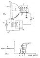
- FIG. 1 there is shown a CRT storage display tube indicated generally as 10 having a display screen or panel 26 and a high energy electron writing gun shown generally as 14.
- the gun is of conventional configuration having a high energy electron source 16 which acts to emit high energy electrons through focusing element 18 to the vertical and horizontal fields created by deflection plates shown at 20, 22 and 24.
- plates 20 and 22 act to vertically deflect the high energy electron beam while plates 24 (only one shown) act to horizontally deflect the electron beam.
- magnetic deflection and magnetic focus can be used.
- the flood gun required by the prior art CRT storage device is absent since in this invention continuous electron beams are not used to generate high brightness display nor to maintain a stored charge pattern.
- the display screen or panel 26 differs from that of the prior art CRT storage device as will be shown later.
- An a.c. sustaining drive field is maintained across display panel 26 by means of a.c. voltage source 28 via leads 27 and 29.
- the a.c. source 28 is a sinusoidal wave generator or an a.c. pulse generator capable of supplying from 0 volts to at least 300 volts.
- a switching arrangement 30 is provided to vary the inductance 25 of resonant circuit 23 according to the capacitive load of the panel 26 in a manner to be described in more detail later.
- the switch 30 is itself controlled by means of a conventional switching circuit 31 itself controlled from the tube control grid in order to vary the inductance in accordance with the energisation of the control grid 16.
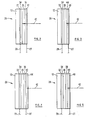
- the display panel shown in Figure 2 consists of a glass face-plate 12 having deposited, or otherwise formed, thereon a transparent contiguous conductive layer 32 of, for example, Sn0 2 or In 2 0 3 .
- a transparent contiguous layer 34 of an insulating material such as BaTi0 3 , SrTi0 3 , AI 2 0 3 , Y z 0 3 , Si 3 N 4 or AIN is formed on the conductive layer 32.
- An electroluminescent layer 36 is formed on the insulating layer 34.
- the electroluminescent layer may comprise any of a variety of well known electroluminescent materials, preferably it is in the form of an electroluminescent polycrystalline thin film, for example, Cu or Mn doped ZnS.
- a second insulating layer 38 is formed contiguous with layer 36 and can be of the same or different material as insulating layer 34.
- a second conductive layer 40 is formed on insulating layer 38. This layer may be either a transparent or non-transparent thin film of Sn0 2 , In 2 0 3 , Al, Cu, Ag, Au or other thin metal layers. Likewise thin layers of copper iodide or graphite can be employed.
- the display panel shown in Figure 3 is similar to that shown in Figure 2 except that the second insulating layer 38 is replaced by a layer 44 of a material which is both insulating and cathodoluminescent.
- electroluminescent materials exhibit electroluminescence in response to an applied a.c. field
- cathodoluminescent materials exhibit luminescence in response to direct electron beam or ultra violet radiation.
- the material selected generally emits light in the ultra violet and blue wavelenghts of the spectrum in response to electron beam radiation.
- AIN which is an efficient ultra-violet light emitter.
- Many other wide band gap materials such as metal oxides and metal tungstates may also be used.
- the remaining layers are identical to corresponding layers in the panel shown in Figure 2 and are identified by the same reference numerals.
- the display panel shown in Figure 4 is again similar to that shown in Figure 2 with the addition of a catholuminescent phosphor layer 44 on the second conductive layer 40.
- Examples of cathodoluminescent phosphors which may be used in the present invention include lead doped barium zinc magnesium silicate, lead doped strontium hexaborate, copper doped zinc cadmium sulphide, manganese doped zinc silicate, silver doped zinc sulphide, zinc doped zinc oxide and the like.
- the display panel shown in Figure 5 is similar to that of Figure 4. In this arrangement, the cathodoluminescent layer 44 and the second conductive layer 40 are interchanged.
- the a.c. sustained voltage, V s from the a.c. source 28 is applied across the electroluminescent layer 36 by means of conductive layers 32 and 40 which are connected to conductors 29 and 27 respectively.
- Figure 6 shows a curve of brightness B against applied voltage V (RMS) showing that the electroluminescent material exhibits hysteresis characteristics.
- the drive voltage level V s is therefore selected to lie above the extinction voltage, V and below the turn-on threshold voltage, V, for the material.
- the intensity of light output from the electroluminescent material can be selected by radiation with an electron beam or ultra-violet of appropriate magnitude.
- the application of exciting electrons switches the material from one stable state B, where the light output is substantially zero, to another one of a plurality of stable states such as indicated at C, where the light output is relatively high.
- the electroluminescent output can be selected to lie at any value between zero and saturation for the material.
- the threshold voltage V t for electroluminescent materials is typically 50 V to 300 V (RMS) and the extinction voltage V a is typically 0 to 270 V (RMS) depending on the layer thickness of the electroluminescent device.
- the panel shown in Figure 2 operates directly by the penetration of electrons, illustrated by arrow 42, to electroluminescent layer 36. Such penetration activates the storage mechanism. It is thought that the incoming electrons or the secondary electrons and light radiation induced by the electron beam excite the trapping states or charge storage levels in the electroluminescent material. The excited charges are polarised under the sustaining drive field to result in an internal field. The internal field aids the external field in exciting the electroluminescence. With the panel shown in Figure 3, the electron beam (42) penetrates only to insulating cathodoluminescent layer 44 which emits high energy photons. These high energy photons then activate the electroluminescent storage mechanism in layer 36.
- the electron beam 42 penetrates only to cathodoluminescent layer 44 whereby said layer 44 is caused to emit high energy photons which in turn activate the electroluminescent storage mechanism in layer 36.
- the interchanged cathodoluminescent and conductive layers in the panel shown in Figure 5 provide a trade-off between low energy electrons and ease of activating the electroluminescent layer 36.
- the drive voltage is not sufficient to cause any appreciable electroluminescence before electron excitations.
- the conductivity of the electroluminescent layer 36 is increased (or viewed as the threshold voltage is decreased) so that more current is flowing through and more light emission occurs.
- the higher current flow also establishes an internal polarisation which aids the a.c. voltage in phase to generate more electroluminescence.
- the device is switched to the higher conducting state and through the internal polarisation field (switched in phase with external applied field) the device operates in a stable memory state.
- the sustaining a.c. voltage can be supplied by a sinusoidal wave generator or an a.c. pulse generator. Since the electroluminescent device is a capacitive load, it is advantageous as previously mentioned to arrange for the device to be included as part of a resonant circuit 23 ( Figure 1) in series with the voltage driver 28.
- the inductance 25 of the circuit can be varied according to the capacitive load of panel 26, i.e. proportional to the area of faceplate which is turned on.
- One method of obtaining this type of resonant tuning is to monitor the CRT grid voltage. When the grid voltage is in an off mode no electrons can be emitted out of the CRT gun 14 thus no faceplate area can be excited or turned on.
Landscapes
- Control Of Indicators Other Than Cathode Ray Tubes (AREA)
- Electroluminescent Light Sources (AREA)
- Illuminated Signs And Luminous Advertising (AREA)
- Cathode-Ray Tubes And Fluorescent Screens For Display (AREA)
Claims (9)
Applications Claiming Priority (2)
| Application Number | Priority Date | Filing Date | Title |
|---|---|---|---|
| US807753 | 1977-06-17 | ||
| US05/807,753 US4149108A (en) | 1977-06-17 | 1977-06-17 | Multistable cathode ray type storage display device |
Publications (2)
| Publication Number | Publication Date |
|---|---|
| EP0000613A1 EP0000613A1 (de) | 1979-02-07 |
| EP0000613B1 true EP0000613B1 (de) | 1982-05-12 |
Family
ID=25197101
Family Applications (1)
| Application Number | Title | Priority Date | Filing Date |
|---|---|---|---|
| EP78300019A Expired EP0000613B1 (de) | 1977-06-17 | 1978-06-06 | Kathodenstrahlröhre-Speichervorrichtung mit Elektrolumineszenz-Bildschirm |
Country Status (5)
| Country | Link |
|---|---|
| US (1) | US4149108A (de) |
| EP (1) | EP0000613B1 (de) |
| JP (1) | JPS547270A (de) |
| CA (1) | CA1101125A (de) |
| DE (1) | DE2861805D1 (de) |
Families Citing this family (5)
| Publication number | Priority date | Publication date | Assignee | Title |
|---|---|---|---|---|
| US4249133A (en) * | 1978-07-10 | 1981-02-03 | Tektronix, Inc. | Electroluminescent cathode ray storage tube |
| GB2050777A (en) * | 1979-05-29 | 1981-01-07 | Tektronix Inc | Electroluminescent Storage CRT Display Device and Operating Method |
| US4369393A (en) * | 1980-11-28 | 1983-01-18 | W. H. Brady Co. | Electroluminescent display including semiconductor convertible to insulator |
| FR2513438A1 (fr) * | 1981-09-22 | 1983-03-25 | Thomson Csf | Tube intensificateur d'images a memoire et mode de mise en oeuvre |
| US9595623B1 (en) * | 2014-02-27 | 2017-03-14 | Rockwell Collins, Inc. | PCSS-based semiconductor device, switching device, and method |
Family Cites Families (10)
| Publication number | Priority date | Publication date | Assignee | Title |
|---|---|---|---|---|
| GB818106A (en) * | 1957-02-25 | 1959-08-12 | Gen Electric Co Ltd | Improvements in or relating to cathode ray tubes |
| US2733367A (en) * | 1956-01-31 | Electroluminescent lamp structures | ||
| GB824242A (en) * | 1954-10-21 | 1959-11-25 | Thorn Electrical Ind Ltd | Improvements in and relating to apparatus embodying electroluminescent devices |
| GB877517A (en) * | 1959-07-08 | 1961-09-13 | Ferranti Ltd | Improvements relating to direct-viewing cathode-ray storage tubes |
| US3173057A (en) * | 1961-05-09 | 1965-03-09 | Westinghouse Electric Corp | Electroluminescent combination |
| US3398021A (en) * | 1965-03-23 | 1968-08-20 | Hughes Aircraft Co | Method of making thin film field sustained conductivity device |
| FR1543309A (fr) * | 1966-09-29 | 1968-10-25 | Xerox Corp | Panneau d'affichage électroluminescent |
| US3749977A (en) * | 1970-12-29 | 1973-07-31 | Intern Scanning Devices Inc | Electroluminescent device |
| US3796909A (en) * | 1972-06-15 | 1974-03-12 | Ibm | Electroluminescent storage display |
| JPS53112085A (en) * | 1977-03-10 | 1978-09-30 | Sharp Corp | Thin film el display device |
-
1977
- 1977-06-17 US US05/807,753 patent/US4149108A/en not_active Expired - Lifetime
-
1978
- 1978-03-28 CA CA299,859A patent/CA1101125A/en not_active Expired
- 1978-04-28 JP JP5021678A patent/JPS547270A/ja active Granted
- 1978-06-06 EP EP78300019A patent/EP0000613B1/de not_active Expired
- 1978-06-06 DE DE7878300019T patent/DE2861805D1/de not_active Expired
Also Published As
| Publication number | Publication date |
|---|---|
| JPS5733825B2 (de) | 1982-07-19 |
| DE2861805D1 (en) | 1982-07-01 |
| US4149108A (en) | 1979-04-10 |
| JPS547270A (en) | 1979-01-19 |
| EP0000613A1 (de) | 1979-02-07 |
| CA1101125A (en) | 1981-05-12 |
Similar Documents
| Publication | Publication Date | Title |
|---|---|---|
| KR100401281B1 (ko) | 다이오드구조평판디스플레이 | |
| US5455489A (en) | Displays comprising doped nanocrystal phosphors | |
| EP0003250B1 (de) | Vielfarbige elektrolumineszierende Anzeigevorrichtung | |
| US5955833A (en) | Field emission display devices | |
| EP0000613B1 (de) | Kathodenstrahlröhre-Speichervorrichtung mit Elektrolumineszenz-Bildschirm | |
| US5489817A (en) | Electron-optical terminal image device based on a cold cathode | |
| US5945777A (en) | Surface conduction emitters for use in field emission display devices | |
| US5045754A (en) | Planar light source | |
| US5949185A (en) | Field emission display devices | |
| US3796909A (en) | Electroluminescent storage display | |
| US3908148A (en) | Electro-optical transducer and storage tube | |
| GB2064861A (en) | Erasure method for electroluminescent display devices | |
| US4801850A (en) | High brightness vacuum fluorescent display (VFD) devices | |
| CA1129116A (en) | Electroluminescent cathode ray storage tube | |
| US3749972A (en) | Image display panel | |
| EP0163351B1 (de) | Dünnfilm-Elektrolumineszenzanordnung | |
| Kazan | Materials aspects of display devices | |
| Henisch | Electroluminescent devices | |
| JPH0251891A (ja) | 薄膜el素子 | |
| JPS6323640B2 (de) | ||
| Tannas Jr | Electroluminescent displays | |
| Miller et al. | Electroluminescent display technology | |
| JPS6089098A (ja) | 薄膜el素子の電極構造 | |
| US3313881A (en) | Frequency-dependent color television display | |
| JPH0451490A (ja) | 有機薄膜型電界発光素子の駆動方法 |
Legal Events
| Date | Code | Title | Description |
|---|---|---|---|
| PUAI | Public reference made under article 153(3) epc to a published international application that has entered the european phase |
Free format text: ORIGINAL CODE: 0009012 |
|
| AK | Designated contracting states |
Designated state(s): DE FR GB |
|
| 17P | Request for examination filed | ||
| GRAA | (expected) grant |
Free format text: ORIGINAL CODE: 0009210 |
|
| AK | Designated contracting states |
Designated state(s): DE FR GB |
|
| REF | Corresponds to: |
Ref document number: 2861805 Country of ref document: DE Date of ref document: 19820701 |
|
| PGFP | Annual fee paid to national office [announced via postgrant information from national office to epo] |
Ref country code: FR Payment date: 19840605 Year of fee payment: 7 |
|
| PGFP | Annual fee paid to national office [announced via postgrant information from national office to epo] |
Ref country code: DE Payment date: 19840619 Year of fee payment: 7 |
|
| PG25 | Lapsed in a contracting state [announced via postgrant information from national office to epo] |
Ref country code: GB Effective date: 19890606 |
|
| GBPC | Gb: european patent ceased through non-payment of renewal fee | ||
| PG25 | Lapsed in a contracting state [announced via postgrant information from national office to epo] |
Ref country code: FR Free format text: LAPSE BECAUSE OF NON-PAYMENT OF DUE FEES Effective date: 19900228 |
|
| PG25 | Lapsed in a contracting state [announced via postgrant information from national office to epo] |
Ref country code: DE Effective date: 19900301 |
|
| REG | Reference to a national code |
Ref country code: FR Ref legal event code: ST |
|
| PLBE | No opposition filed within time limit |
Free format text: ORIGINAL CODE: 0009261 |
|
| STAA | Information on the status of an ep patent application or granted ep patent |
Free format text: STATUS: NO OPPOSITION FILED WITHIN TIME LIMIT |