DE102009057566A1 - Vorrichtung für ein Laserabhebeverfahren und Laserabhebeverfahren - Google Patents
Vorrichtung für ein Laserabhebeverfahren und Laserabhebeverfahren Download PDFInfo
- Publication number
- DE102009057566A1 DE102009057566A1 DE102009057566A DE102009057566A DE102009057566A1 DE 102009057566 A1 DE102009057566 A1 DE 102009057566A1 DE 102009057566 A DE102009057566 A DE 102009057566A DE 102009057566 A DE102009057566 A DE 102009057566A DE 102009057566 A1 DE102009057566 A1 DE 102009057566A1
- Authority
- DE
- Germany
- Prior art keywords
- partial beams
- carrier
- semiconductor layer
- laser radiation
- laser
- Prior art date
- Legal status (The legal status is an assumption and is not a legal conclusion. Google has not performed a legal analysis and makes no representation as to the accuracy of the status listed.)
- Withdrawn
Links
Images

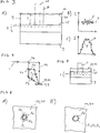
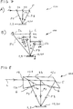
Classifications
-
- B—PERFORMING OPERATIONS; TRANSPORTING
- B23—MACHINE TOOLS; METAL-WORKING NOT OTHERWISE PROVIDED FOR
- B23K—SOLDERING OR UNSOLDERING; WELDING; CLADDING OR PLATING BY SOLDERING OR WELDING; CUTTING BY APPLYING HEAT LOCALLY, e.g. FLAME CUTTING; WORKING BY LASER BEAM
- B23K26/00—Working by laser beam, e.g. welding, cutting or boring
- B23K26/02—Positioning or observing the workpiece, e.g. with respect to the point of impact; Aligning, aiming or focusing the laser beam
- B23K26/06—Shaping the laser beam, e.g. by masks or multi-focusing
- B23K26/0604—Shaping the laser beam, e.g. by masks or multi-focusing by a combination of beams
- B23K26/0608—Shaping the laser beam, e.g. by masks or multi-focusing by a combination of beams in the same heat affected zone [HAZ]
-
- B—PERFORMING OPERATIONS; TRANSPORTING
- B23—MACHINE TOOLS; METAL-WORKING NOT OTHERWISE PROVIDED FOR
- B23K—SOLDERING OR UNSOLDERING; WELDING; CLADDING OR PLATING BY SOLDERING OR WELDING; CUTTING BY APPLYING HEAT LOCALLY, e.g. FLAME CUTTING; WORKING BY LASER BEAM
- B23K26/00—Working by laser beam, e.g. welding, cutting or boring
- B23K26/02—Positioning or observing the workpiece, e.g. with respect to the point of impact; Aligning, aiming or focusing the laser beam
- B23K26/06—Shaping the laser beam, e.g. by masks or multi-focusing
- B23K26/062—Shaping the laser beam, e.g. by masks or multi-focusing by direct control of the laser beam
- B23K26/0622—Shaping the laser beam, e.g. by masks or multi-focusing by direct control of the laser beam by shaping pulses
- B23K26/0624—Shaping the laser beam, e.g. by masks or multi-focusing by direct control of the laser beam by shaping pulses using ultrashort pulses, i.e. pulses of 1 ns or less
-
- B—PERFORMING OPERATIONS; TRANSPORTING
- B23—MACHINE TOOLS; METAL-WORKING NOT OTHERWISE PROVIDED FOR
- B23K—SOLDERING OR UNSOLDERING; WELDING; CLADDING OR PLATING BY SOLDERING OR WELDING; CUTTING BY APPLYING HEAT LOCALLY, e.g. FLAME CUTTING; WORKING BY LASER BEAM
- B23K26/00—Working by laser beam, e.g. welding, cutting or boring
- B23K26/02—Positioning or observing the workpiece, e.g. with respect to the point of impact; Aligning, aiming or focusing the laser beam
- B23K26/06—Shaping the laser beam, e.g. by masks or multi-focusing
- B23K26/067—Dividing the beam into multiple beams, e.g. multi-focusing
-
- B—PERFORMING OPERATIONS; TRANSPORTING
- B23—MACHINE TOOLS; METAL-WORKING NOT OTHERWISE PROVIDED FOR
- B23K—SOLDERING OR UNSOLDERING; WELDING; CLADDING OR PLATING BY SOLDERING OR WELDING; CUTTING BY APPLYING HEAT LOCALLY, e.g. FLAME CUTTING; WORKING BY LASER BEAM
- B23K26/00—Working by laser beam, e.g. welding, cutting or boring
- B23K26/02—Positioning or observing the workpiece, e.g. with respect to the point of impact; Aligning, aiming or focusing the laser beam
- B23K26/06—Shaping the laser beam, e.g. by masks or multi-focusing
- B23K26/073—Shaping the laser spot
- B23K26/0736—Shaping the laser spot into an oval shape, e.g. elliptic shape
-
- B—PERFORMING OPERATIONS; TRANSPORTING
- B23—MACHINE TOOLS; METAL-WORKING NOT OTHERWISE PROVIDED FOR
- B23K—SOLDERING OR UNSOLDERING; WELDING; CLADDING OR PLATING BY SOLDERING OR WELDING; CUTTING BY APPLYING HEAT LOCALLY, e.g. FLAME CUTTING; WORKING BY LASER BEAM
- B23K26/00—Working by laser beam, e.g. welding, cutting or boring
- B23K26/16—Removal of by-products, e.g. particles or vapours produced during treatment of a workpiece
-
- B—PERFORMING OPERATIONS; TRANSPORTING
- B23—MACHINE TOOLS; METAL-WORKING NOT OTHERWISE PROVIDED FOR
- B23K—SOLDERING OR UNSOLDERING; WELDING; CLADDING OR PLATING BY SOLDERING OR WELDING; CUTTING BY APPLYING HEAT LOCALLY, e.g. FLAME CUTTING; WORKING BY LASER BEAM
- B23K26/00—Working by laser beam, e.g. welding, cutting or boring
- B23K26/352—Working by laser beam, e.g. welding, cutting or boring for surface treatment
-
- B—PERFORMING OPERATIONS; TRANSPORTING
- B23—MACHINE TOOLS; METAL-WORKING NOT OTHERWISE PROVIDED FOR
- B23K—SOLDERING OR UNSOLDERING; WELDING; CLADDING OR PLATING BY SOLDERING OR WELDING; CUTTING BY APPLYING HEAT LOCALLY, e.g. FLAME CUTTING; WORKING BY LASER BEAM
- B23K26/00—Working by laser beam, e.g. welding, cutting or boring
- B23K26/36—Removing material
- B23K26/361—Removing material for deburring or mechanical trimming
-
- B—PERFORMING OPERATIONS; TRANSPORTING
- B23—MACHINE TOOLS; METAL-WORKING NOT OTHERWISE PROVIDED FOR
- B23K—SOLDERING OR UNSOLDERING; WELDING; CLADDING OR PLATING BY SOLDERING OR WELDING; CUTTING BY APPLYING HEAT LOCALLY, e.g. FLAME CUTTING; WORKING BY LASER BEAM
- B23K26/00—Working by laser beam, e.g. welding, cutting or boring
- B23K26/36—Removing material
- B23K26/40—Removing material taking account of the properties of the material involved
-
- B—PERFORMING OPERATIONS; TRANSPORTING
- B23—MACHINE TOOLS; METAL-WORKING NOT OTHERWISE PROVIDED FOR
- B23K—SOLDERING OR UNSOLDERING; WELDING; CLADDING OR PLATING BY SOLDERING OR WELDING; CUTTING BY APPLYING HEAT LOCALLY, e.g. FLAME CUTTING; WORKING BY LASER BEAM
- B23K26/00—Working by laser beam, e.g. welding, cutting or boring
- B23K26/50—Working by transmitting the laser beam through or within the workpiece
- B23K26/57—Working by transmitting the laser beam through or within the workpiece the laser beam entering a face of the workpiece from which it is transmitted through the workpiece material to work on a different workpiece face, e.g. for effecting removal, fusion splicing, modifying or reforming
-
- B—PERFORMING OPERATIONS; TRANSPORTING
- B23—MACHINE TOOLS; METAL-WORKING NOT OTHERWISE PROVIDED FOR
- B23K—SOLDERING OR UNSOLDERING; WELDING; CLADDING OR PLATING BY SOLDERING OR WELDING; CUTTING BY APPLYING HEAT LOCALLY, e.g. FLAME CUTTING; WORKING BY LASER BEAM
- B23K2101/00—Articles made by soldering, welding or cutting
- B23K2101/36—Electric or electronic devices
- B23K2101/40—Semiconductor devices
-
- B—PERFORMING OPERATIONS; TRANSPORTING
- B23—MACHINE TOOLS; METAL-WORKING NOT OTHERWISE PROVIDED FOR
- B23K—SOLDERING OR UNSOLDERING; WELDING; CLADDING OR PLATING BY SOLDERING OR WELDING; CUTTING BY APPLYING HEAT LOCALLY, e.g. FLAME CUTTING; WORKING BY LASER BEAM
- B23K2103/00—Materials to be soldered, welded or cut
- B23K2103/50—Inorganic materials other than metals or composite materials
-
- H—ELECTRICITY
- H10—SEMICONDUCTOR DEVICES; ELECTRIC SOLID-STATE DEVICES NOT OTHERWISE PROVIDED FOR
- H10H—INORGANIC LIGHT-EMITTING SEMICONDUCTOR DEVICES HAVING POTENTIAL BARRIERS
- H10H20/00—Individual inorganic light-emitting semiconductor devices having potential barriers, e.g. light-emitting diodes [LED]
- H10H20/01—Manufacture or treatment
- H10H20/011—Manufacture or treatment of bodies, e.g. forming semiconductor layers
- H10H20/018—Bonding of wafers
Landscapes
- Physics & Mathematics (AREA)
- Optics & Photonics (AREA)
- Engineering & Computer Science (AREA)
- Plasma & Fusion (AREA)
- Mechanical Engineering (AREA)
- Chemical & Material Sciences (AREA)
- Chemical Kinetics & Catalysis (AREA)
- General Chemical & Material Sciences (AREA)
- Oil, Petroleum & Natural Gas (AREA)
- Laser Beam Processing (AREA)
Priority Applications (8)
| Application Number | Priority Date | Filing Date | Title |
|---|---|---|---|
| DE102009057566A DE102009057566A1 (de) | 2009-12-09 | 2009-12-09 | Vorrichtung für ein Laserabhebeverfahren und Laserabhebeverfahren |
| KR1020127017715A KR20120101707A (ko) | 2009-12-09 | 2010-10-21 | 레이저 박리 방법 그리고 빔 스플리터를 구비하는 레이저 박리 방법용 장치 |
| JP2012542414A JP5635123B2 (ja) | 2009-12-09 | 2010-10-21 | ビームスプリッタを用いたレーザリフトオフ法のための方法および装置 |
| EP10771088.1A EP2509741B9 (de) | 2009-12-09 | 2010-10-21 | Verfahren und vorrichtung für ein laserabhebeverfahren mit einem strahlteiler |
| CN201080055854.XA CN102639281B (zh) | 2009-12-09 | 2010-10-21 | 利用分束器进行激光剥离方法的方法和装置 |
| PCT/EP2010/065891 WO2011069735A1 (de) | 2009-12-09 | 2010-10-21 | Verfahren und vorrichtung für ein laserabhebeverfahren mit einem strahlteiler |
| US13/514,373 US8946098B2 (en) | 2009-12-09 | 2010-10-21 | Device for a laser lift-off method and laser lift-off method |
| TW099140137A TW201143952A (en) | 2009-12-09 | 2010-11-22 | Device for a laser lift-off method and laser lift-off method |
Applications Claiming Priority (1)
| Application Number | Priority Date | Filing Date | Title |
|---|---|---|---|
| DE102009057566A DE102009057566A1 (de) | 2009-12-09 | 2009-12-09 | Vorrichtung für ein Laserabhebeverfahren und Laserabhebeverfahren |
Publications (1)
| Publication Number | Publication Date |
|---|---|
| DE102009057566A1 true DE102009057566A1 (de) | 2011-06-16 |
Family
ID=43416867
Family Applications (1)
| Application Number | Title | Priority Date | Filing Date |
|---|---|---|---|
| DE102009057566A Withdrawn DE102009057566A1 (de) | 2009-12-09 | 2009-12-09 | Vorrichtung für ein Laserabhebeverfahren und Laserabhebeverfahren |
Country Status (8)
| Country | Link |
|---|---|
| US (1) | US8946098B2 (https=) |
| EP (1) | EP2509741B9 (https=) |
| JP (1) | JP5635123B2 (https=) |
| KR (1) | KR20120101707A (https=) |
| CN (1) | CN102639281B (https=) |
| DE (1) | DE102009057566A1 (https=) |
| TW (1) | TW201143952A (https=) |
| WO (1) | WO2011069735A1 (https=) |
Cited By (5)
| Publication number | Priority date | Publication date | Assignee | Title |
|---|---|---|---|---|
| WO2017129795A1 (de) * | 2016-01-29 | 2017-08-03 | Kjellberg-Stiftung | Vorrichtung und verfahren zur thermischen bearbeitung |
| DE102022114637A1 (de) | 2022-06-10 | 2023-12-21 | Trumpf Laser Gmbh | Verfahren und Vorrichtung zum Verarbeiten mindestens eines Teilbereichs eines Schichtsystems |
| DE102022114646A1 (de) | 2022-06-10 | 2023-12-21 | Trumpf Laser Gmbh | Verfahren und Vorrichtung zum Verarbeiten mindestens eines Teilbereichs eines Schichtsystems |
| DE102023201553A1 (de) * | 2023-02-22 | 2024-08-22 | 3D-Micromac Ag | Verfahren und System zur Herstellung mikroelektronischer Komponenten mit Schichtaufbau |
| WO2025078839A1 (en) * | 2023-10-13 | 2025-04-17 | Pulse Investments Uk Limited | Method and system for surface layer removal |
Families Citing this family (13)
| Publication number | Priority date | Publication date | Assignee | Title |
|---|---|---|---|---|
| DE102010030358B4 (de) | 2010-06-22 | 2014-05-22 | Osram Opto Semiconductors Gmbh | Verfahren zum Abtrennen einer Substratscheibe |
| US20140251533A1 (en) * | 2013-03-11 | 2014-09-11 | Samsung Display Co., Ltd. | Substrate peeling device, method for peeling substrate, and method for fabricating flexible display device |
| GB2519088B (en) | 2013-10-08 | 2015-09-16 | M Solv Ltd | Laser scanning system for laser release |
| CN104858544B (zh) | 2014-02-26 | 2018-09-21 | 恩耐公司 | 激光剥离方法及用于在目标上引起激光剥离的系统 |
| CN104158067B (zh) * | 2014-08-22 | 2016-06-22 | 苏州大学 | 一种导线外皮的激光剥离方法 |
| KR20160049382A (ko) | 2014-10-27 | 2016-05-09 | 삼성디스플레이 주식회사 | 레이저 박리 장치 및 표시 장치의 제조 방법 |
| CN104297926A (zh) * | 2014-11-12 | 2015-01-21 | 核工业理化工程研究院 | 高功率激光分光光纤装置 |
| GB201509766D0 (en) * | 2015-06-05 | 2015-07-22 | Element Six Technologies Ltd | Method of fabricating diamond-semiconductor composite substrates |
| DE102018200036B3 (de) * | 2018-01-03 | 2019-01-17 | Fraunhofer-Gesellschaft zur Förderung der angewandten Forschung e.V. | Optische Anordnung zur direkten Laserinterferenzstrukturierung |
| CN109623155B (zh) * | 2018-11-14 | 2020-07-10 | 吉林大学 | 利用多光子激发进行近4π立体角飞秒激光直写加工的方法及应用 |
| DE112020002981A5 (de) * | 2019-06-21 | 2022-03-03 | Trumpf Laser- Und Systemtechnik Gmbh | Verfahren zum Bearbeiten eines Werkstücks |
| CN110491811B (zh) * | 2019-09-19 | 2024-06-14 | 北京大学东莞光电研究院 | 一种可调节光强型激光剥离装置 |
| DE102024209847A1 (de) * | 2024-10-10 | 2026-04-16 | Carl Zeiss Smt Gmbh | Verfahren und Vorrichtung zur Erzeugung von Materialabtragungsbereichen in einem Glasobjekt |
Citations (3)
| Publication number | Priority date | Publication date | Assignee | Title |
|---|---|---|---|---|
| EP0859261A1 (en) * | 1997-02-04 | 1998-08-19 | Miyachi Technos Corporation | Laser beam-splitting apparatus |
| US6169631B1 (en) * | 1998-05-19 | 2001-01-02 | Seagate Technology Llc | Laser-texturing data zone on a magnetic disk surface by using degenerative two wave mixing |
| US6210479B1 (en) * | 1999-02-26 | 2001-04-03 | International Business Machines Corporation | Product and process for forming a semiconductor structure on a host substrate |
Family Cites Families (9)
| Publication number | Priority date | Publication date | Assignee | Title |
|---|---|---|---|---|
| JPH06296597A (ja) | 1992-08-19 | 1994-10-25 | D F C:Kk | 脳波分析方法及びその装置 |
| US5786560A (en) * | 1995-03-31 | 1998-07-28 | Panasonic Technologies, Inc. | 3-dimensional micromachining with femtosecond laser pulses |
| CN2432001Y (zh) * | 2000-06-21 | 2001-05-30 | 中国科学院光电技术研究所 | 一种激光干涉光刻系统 |
| TWI226139B (en) * | 2002-01-31 | 2005-01-01 | Osram Opto Semiconductors Gmbh | Method to manufacture a semiconductor-component |
| JP4662918B2 (ja) | 2003-01-31 | 2011-03-30 | オスラム オプト セミコンダクターズ ゲゼルシャフト ミット ベシュレンクテル ハフツング | 半導体構成素子の製造のための方法 |
| JP4423465B2 (ja) | 2004-02-12 | 2010-03-03 | 住友重機械工業株式会社 | レーザ加工方法及びレーザ加工装置 |
| DE602006004913D1 (de) * | 2005-04-28 | 2009-03-12 | Semiconductor Energy Lab | Verfahren und Vorrichtung zur Herstellung von Halbleitern mittels Laserstrahlung |
| US7829909B2 (en) | 2005-11-15 | 2010-11-09 | Verticle, Inc. | Light emitting diodes and fabrication methods thereof |
| CN101434005B (zh) | 2008-11-20 | 2011-05-25 | 武汉凌云光电科技有限责任公司 | 多通道非晶硅太阳能板激光刻膜机 |
-
2009
- 2009-12-09 DE DE102009057566A patent/DE102009057566A1/de not_active Withdrawn
-
2010
- 2010-10-21 CN CN201080055854.XA patent/CN102639281B/zh not_active Expired - Fee Related
- 2010-10-21 EP EP10771088.1A patent/EP2509741B9/de not_active Not-in-force
- 2010-10-21 KR KR1020127017715A patent/KR20120101707A/ko not_active Withdrawn
- 2010-10-21 WO PCT/EP2010/065891 patent/WO2011069735A1/de not_active Ceased
- 2010-10-21 US US13/514,373 patent/US8946098B2/en not_active Expired - Fee Related
- 2010-10-21 JP JP2012542414A patent/JP5635123B2/ja not_active Expired - Fee Related
- 2010-11-22 TW TW099140137A patent/TW201143952A/zh unknown
Patent Citations (3)
| Publication number | Priority date | Publication date | Assignee | Title |
|---|---|---|---|---|
| EP0859261A1 (en) * | 1997-02-04 | 1998-08-19 | Miyachi Technos Corporation | Laser beam-splitting apparatus |
| US6169631B1 (en) * | 1998-05-19 | 2001-01-02 | Seagate Technology Llc | Laser-texturing data zone on a magnetic disk surface by using degenerative two wave mixing |
| US6210479B1 (en) * | 1999-02-26 | 2001-04-03 | International Business Machines Corporation | Product and process for forming a semiconductor structure on a host substrate |
Cited By (6)
| Publication number | Priority date | Publication date | Assignee | Title |
|---|---|---|---|---|
| WO2017129795A1 (de) * | 2016-01-29 | 2017-08-03 | Kjellberg-Stiftung | Vorrichtung und verfahren zur thermischen bearbeitung |
| US11224939B2 (en) | 2016-01-29 | 2022-01-18 | Kjellberg-Stiftung | Apparatus for thermal processing |
| DE102022114637A1 (de) | 2022-06-10 | 2023-12-21 | Trumpf Laser Gmbh | Verfahren und Vorrichtung zum Verarbeiten mindestens eines Teilbereichs eines Schichtsystems |
| DE102022114646A1 (de) | 2022-06-10 | 2023-12-21 | Trumpf Laser Gmbh | Verfahren und Vorrichtung zum Verarbeiten mindestens eines Teilbereichs eines Schichtsystems |
| DE102023201553A1 (de) * | 2023-02-22 | 2024-08-22 | 3D-Micromac Ag | Verfahren und System zur Herstellung mikroelektronischer Komponenten mit Schichtaufbau |
| WO2025078839A1 (en) * | 2023-10-13 | 2025-04-17 | Pulse Investments Uk Limited | Method and system for surface layer removal |
Also Published As
| Publication number | Publication date |
|---|---|
| JP5635123B2 (ja) | 2014-12-03 |
| US8946098B2 (en) | 2015-02-03 |
| EP2509741B9 (de) | 2015-02-25 |
| US20120258605A1 (en) | 2012-10-11 |
| JP2013513487A (ja) | 2013-04-22 |
| EP2509741B1 (de) | 2014-12-03 |
| CN102639281B (zh) | 2015-02-25 |
| TW201143952A (en) | 2011-12-16 |
| WO2011069735A1 (de) | 2011-06-16 |
| EP2509741A1 (de) | 2012-10-17 |
| KR20120101707A (ko) | 2012-09-14 |
| CN102639281A (zh) | 2012-08-15 |
Similar Documents
| Publication | Publication Date | Title |
|---|---|---|
| EP2509741B1 (de) | Verfahren und vorrichtung für ein laserabhebeverfahren mit einem strahlteiler | |
| DE112014001696B4 (de) | Laserbearbeitungsvorrichtung und Laserbearbeitungsverfahren | |
| DE112014001676B4 (de) | Laserbearbeitungsvorrichtung und Laserbearbeitungsverfahren | |
| DE112015002536B4 (de) | Laserbearbeitungsvorrichtung und Laserbearbeitungsverfahren | |
| DE112014001653B4 (de) | Laserbearbeitungsvorrichtung und Laserbearbeitungsverfahren | |
| DE102014201193B4 (de) | Laserbearbeitungsverfahren | |
| DE112015001612T5 (de) | Laserbearbeitungseinrichtung und Laserbearbeitungsverfahren | |
| DE102018126381A1 (de) | Verfahren und Vorrichtung zum Einfügen einer Trennlinie in ein transparentes sprödbrüchiges Material, sowie verfahrensgemäß herstellbares, mit einer Trennlinie versehenes Element | |
| DE112014001688T5 (de) | Laserbearbeitungsvorrichtung und Laserbearbeitungsverfahren | |
| DE112015002529T5 (de) | Laserbearbeitungsvorrichtung und Laserbearbeitungsverfahren | |
| DE202014011497U1 (de) | Laserbearbeitungsvorrichtung | |
| DE102020102077B4 (de) | Laserbearbeitungsvorrichtung und Verfahren zur Laserbearbeitung eines Werkstücks | |
| DE102020107760A1 (de) | Laserbearbeitungsvorrichtung und Verfahren zur Laserbearbeitung eines Werkstücks | |
| EP3860798B1 (de) | Laserbearbeitungssystem | |
| DE112009003752T5 (de) | Laserbearbeitungsvorrichtung, Laserbearbeitungsverfahren und Herstellungsverfahren einer Fotovoltaikvorrichtung | |
| EP3589989B1 (de) | Verfahren zur korrektur eines reflektiven optischen elements für den wellenlängenbereich von 5 nm bis 20 nm | |
| DE102019205847B4 (de) | Verfahren und Vorrichtung zur Erzeugung mindestens einer Modifikation in einem Festkörper | |
| DE102020127116B4 (de) | Vorrichtung und Verfahren zum Laserbearbeiten eines Werkstücks | |
| DE112016004432T5 (de) | Laserbearbeitungsverfahren und Laserbearbeitungsvorrichtung | |
| DE102015004347A1 (de) | Erzeugung von physischen Modifikationen mittels LASER im Inneren eines Festkörpers | |
| DE102007020704B4 (de) | Einrichtung für die Bearbeitung eines Werkstückes mit einem Laserstrahl | |
| DE102019118676A1 (de) | Optisches System zur Homogenisierung der Intensität von Lichtstrahlung | |
| DE102023201553A1 (de) | Verfahren und System zur Herstellung mikroelektronischer Komponenten mit Schichtaufbau | |
| DE102008056315A1 (de) | Vorrichtung zur Homogenisierung von Laserstrahlung sowie Vorrichtung zur Formung von Laserstrahlung | |
| DE102022114637A1 (de) | Verfahren und Vorrichtung zum Verarbeiten mindestens eines Teilbereichs eines Schichtsystems |
Legal Events
| Date | Code | Title | Description |
|---|---|---|---|
| OM8 | Search report available as to paragraph 43 lit. 1 sentence 1 patent law | ||
| R119 | Application deemed withdrawn, or ip right lapsed, due to non-payment of renewal fee |