DE102009033686A1 - Optoelectronic semiconductor component and method for producing an inorganic optoelectronic semiconductor component - Google Patents
Optoelectronic semiconductor component and method for producing an inorganic optoelectronic semiconductor component Download PDFInfo
- Publication number
- DE102009033686A1 DE102009033686A1 DE102009033686A DE102009033686A DE102009033686A1 DE 102009033686 A1 DE102009033686 A1 DE 102009033686A1 DE 102009033686 A DE102009033686 A DE 102009033686A DE 102009033686 A DE102009033686 A DE 102009033686A DE 102009033686 A1 DE102009033686 A1 DE 102009033686A1
- Authority
- DE
- Germany
- Prior art keywords
- layer
- metal mirror
- layer sequence
- semiconductor layer
- carrier
- Prior art date
- Legal status (The legal status is an assumption and is not a legal conclusion. Google has not performed a legal analysis and makes no representation as to the accuracy of the status listed.)
- Withdrawn
Links
Images

Classifications
-
- H—ELECTRICITY
- H01—ELECTRIC ELEMENTS
- H01L—SEMICONDUCTOR DEVICES NOT COVERED BY CLASS H10
- H01L33/00—Semiconductor devices with at least one potential-jump barrier or surface barrier specially adapted for light emission; Processes or apparatus specially adapted for the manufacture or treatment thereof or of parts thereof; Details thereof
- H01L33/44—Semiconductor devices with at least one potential-jump barrier or surface barrier specially adapted for light emission; Processes or apparatus specially adapted for the manufacture or treatment thereof or of parts thereof; Details thereof characterised by the coatings, e.g. passivation layer or anti-reflective coating
-
- H—ELECTRICITY
- H01—ELECTRIC ELEMENTS
- H01L—SEMICONDUCTOR DEVICES NOT COVERED BY CLASS H10
- H01L24/00—Arrangements for connecting or disconnecting semiconductor or solid-state bodies; Methods or apparatus related thereto
- H01L24/01—Means for bonding being attached to, or being formed on, the surface to be connected, e.g. chip-to-package, die-attach, "first-level" interconnects; Manufacturing methods related thereto
- H01L24/02—Bonding areas ; Manufacturing methods related thereto
- H01L24/04—Structure, shape, material or disposition of the bonding areas prior to the connecting process
- H01L24/05—Structure, shape, material or disposition of the bonding areas prior to the connecting process of an individual bonding area
-
- H—ELECTRICITY
- H01—ELECTRIC ELEMENTS
- H01L—SEMICONDUCTOR DEVICES NOT COVERED BY CLASS H10
- H01L2224/00—Indexing scheme for arrangements for connecting or disconnecting semiconductor or solid-state bodies and methods related thereto as covered by H01L24/00
- H01L2224/01—Means for bonding being attached to, or being formed on, the surface to be connected, e.g. chip-to-package, die-attach, "first-level" interconnects; Manufacturing methods related thereto
- H01L2224/02—Bonding areas; Manufacturing methods related thereto
- H01L2224/04—Structure, shape, material or disposition of the bonding areas prior to the connecting process
- H01L2224/04042—Bonding areas specifically adapted for wire connectors, e.g. wirebond pads
-
- H—ELECTRICITY
- H01—ELECTRIC ELEMENTS
- H01L—SEMICONDUCTOR DEVICES NOT COVERED BY CLASS H10
- H01L2224/00—Indexing scheme for arrangements for connecting or disconnecting semiconductor or solid-state bodies and methods related thereto as covered by H01L24/00
- H01L2224/01—Means for bonding being attached to, or being formed on, the surface to be connected, e.g. chip-to-package, die-attach, "first-level" interconnects; Manufacturing methods related thereto
- H01L2224/02—Bonding areas; Manufacturing methods related thereto
- H01L2224/04—Structure, shape, material or disposition of the bonding areas prior to the connecting process
- H01L2224/05—Structure, shape, material or disposition of the bonding areas prior to the connecting process of an individual bonding area
- H01L2224/0554—External layer
- H01L2224/0555—Shape
- H01L2224/05556—Shape in side view
-
- H—ELECTRICITY
- H01—ELECTRIC ELEMENTS
- H01L—SEMICONDUCTOR DEVICES NOT COVERED BY CLASS H10
- H01L2224/00—Indexing scheme for arrangements for connecting or disconnecting semiconductor or solid-state bodies and methods related thereto as covered by H01L24/00
- H01L2224/01—Means for bonding being attached to, or being formed on, the surface to be connected, e.g. chip-to-package, die-attach, "first-level" interconnects; Manufacturing methods related thereto
- H01L2224/42—Wire connectors; Manufacturing methods related thereto
- H01L2224/47—Structure, shape, material or disposition of the wire connectors after the connecting process
- H01L2224/48—Structure, shape, material or disposition of the wire connectors after the connecting process of an individual wire connector
- H01L2224/4805—Shape
- H01L2224/4809—Loop shape
- H01L2224/48091—Arched
-
- H—ELECTRICITY
- H01—ELECTRIC ELEMENTS
- H01L—SEMICONDUCTOR DEVICES NOT COVERED BY CLASS H10
- H01L2924/00—Indexing scheme for arrangements or methods for connecting or disconnecting semiconductor or solid-state bodies as covered by H01L24/00
- H01L2924/10—Details of semiconductor or other solid state devices to be connected
- H01L2924/11—Device type
- H01L2924/12—Passive devices, e.g. 2 terminal devices
- H01L2924/1204—Optical Diode
- H01L2924/12041—LED
-
- H—ELECTRICITY
- H01—ELECTRIC ELEMENTS
- H01L—SEMICONDUCTOR DEVICES NOT COVERED BY CLASS H10
- H01L2924/00—Indexing scheme for arrangements or methods for connecting or disconnecting semiconductor or solid-state bodies as covered by H01L24/00
- H01L2924/10—Details of semiconductor or other solid state devices to be connected
- H01L2924/11—Device type
- H01L2924/12—Passive devices, e.g. 2 terminal devices
- H01L2924/1204—Optical Diode
- H01L2924/12043—Photo diode
-
- H—ELECTRICITY
- H01—ELECTRIC ELEMENTS
- H01L—SEMICONDUCTOR DEVICES NOT COVERED BY CLASS H10
- H01L2933/00—Details relating to devices covered by the group H01L33/00 but not provided for in its subgroups
- H01L2933/0008—Processes
- H01L2933/0025—Processes relating to coatings
-
- H—ELECTRICITY
- H01—ELECTRIC ELEMENTS
- H01L—SEMICONDUCTOR DEVICES NOT COVERED BY CLASS H10
- H01L33/00—Semiconductor devices with at least one potential-jump barrier or surface barrier specially adapted for light emission; Processes or apparatus specially adapted for the manufacture or treatment thereof or of parts thereof; Details thereof
- H01L33/36—Semiconductor devices with at least one potential-jump barrier or surface barrier specially adapted for light emission; Processes or apparatus specially adapted for the manufacture or treatment thereof or of parts thereof; Details thereof characterised by the electrodes
- H01L33/40—Materials therefor
- H01L33/405—Reflective materials
Abstract
In mindestens einer Ausführungsform des optoelektronischen Halbleiterbauteils (1) beinhaltet dieses einen Träger (2) und mindestens eine Halbleiterschichtenfolge (3). Die Halbleiterschichtenfolge (3) weist zumindest eine aktive Schicht (30) auf. Die Halbleiterschichtenfolge (3) ist ferner an dem Träger (2) angebracht. Weiterhin beinhaltet das Halbleiterbauteil (1) einen Metallspiegel (4), der sich zwischen dem Träger (2) und der Halbleiterschichtenfolge (3) befindet. Der Träger (2) und die Halbleiterschichtenfolge (3) überragen den Metallspiegel (4) in lateraler Richtung. Außerdem ist der Metallspiegel (4) in lateraler Richtung unmittelbar von einer strahlungsdurchlässigen und elektrisch isolierenden Verkapselungsschicht (5) umgeben.In at least one embodiment of the optoelectronic semiconductor component (1), the latter comprises a carrier (2) and at least one semiconductor layer sequence (3). The semiconductor layer sequence (3) has at least one active layer (30). The semiconductor layer sequence (3) is also attached to the carrier (2). Furthermore, the semiconductor component (1) contains a metal mirror (4), which is located between the carrier (2) and the semiconductor layer sequence (3). The carrier (2) and the semiconductor layer sequence (3) project beyond the metal mirror (4) in the lateral direction. In addition, the metal mirror (4) is directly surrounded in the lateral direction by a radiation-permeable and electrically insulating encapsulation layer (5).
Description
Es wird ein optoelektronisches Halbleiterbauteil angegeben. Darüber hinaus wird ein Verfahren zur Herstellung eines anorganischen optoelektronischen Halbleiterbauteils angegeben.It an optoelectronic semiconductor device is specified. About that In addition, a method for producing an inorganic optoelectronic Semiconductor device specified.
Eine zu lösende Aufgabe besteht darin, ein optoelektronisches Halbleiterbauteil mit einer hohen Lichtauskoppeleffizienz anzugeben. Eine weitere zu lösende Aufgabe besteht darin, ein Verfahren zur Herstellung eines solchen optoelektronischen Halbleiterbauteils anzugeben.A to be solved task is an optoelectronic Specify semiconductor device with a high Lichtauskoppeleffizienz. Another object to be solved is a method for producing such an optoelectronic semiconductor device specify.
Gemäß zumindest
einer Ausführungsform des optoelektronischen Halbleiterbauteils
beinhaltet dieses mindestens eine Halbleiterschichtenfolge. Bei der
bevorzugt anorganischen Halbleiterschichtenfolge kann es sich um
eine Leuchtdiode, um eine Laserdiode oder um eine Fotodiode handeln.
Bevorzugt ist die Halbleiterschichtenfolge eine Dünnfilmschichtenfolge,
wie beispielsweise in der Druckschrift
Gemäß zumindest einer Ausführungsform des optoelektronischen Halbleiterbauteils umfasst dieses einen Träger. Der Träger ist bevorzugt dazu eingerichtet, die Halbleiterschichtenfolge zu tragen und mechanisch zu stützen. Bei dem Träger handelt es sich insbesondere um einen rigiden, im Rahmen der im verwendungsgemäßen Betrieb des Halbleiterbauteils auftretenden Belastungen biegestabilen Festkörper. Beispielsweise umfasst oder besteht der Träger aus einem Halbleitermaterial wie Germanium oder Silizium, aus einem Metall wie Cu, Ni, Ag oder Mo oder aus einem elektrisch isolierenden Material wie Al2O3, AlN oder SiNx. Der Träger kann von einem Aufwachssubstrat der Halbleiterschichtenfolge verschieden sein.According to at least one embodiment of the optoelectronic semiconductor component, this comprises a carrier. The carrier is preferably configured to carry and mechanically support the semiconductor layer sequence. The carrier is in particular a rigid, bending-resistant solid material in the context of the loads occurring in the operation according to the invention of the semiconductor component. For example, the support comprises or consists of a semiconductor material such as germanium or silicon, of a metal such as Cu, Ni, Ag or Mo or of an electrically insulating material such as Al 2 O 3 , AlN or SiN x . The carrier may be different from a growth substrate of the semiconductor layer sequence.
Gemäß zumindest einer Ausführungsform des optoelektronischen Halbleiterbauteils ist die Halbleiterschichtenfolge an dem Träger angebracht. Das kann bedeuten, dass sich zwischen der Halbleiterschichtenfolge und dem Träger eine oder mehrere Schichten befinden, über die eine Haftvermittlung und eine feste Verbindung zwischen der Halbleiterschichtenfolge und dem Träger gewährleistet ist.At least an embodiment of the optoelectronic semiconductor device the semiconductor layer sequence is attached to the carrier. The may mean that between the semiconductor layer sequence and the carrier one or more layers over the one adhesion and a firm connection between the Semiconductor layer sequence and the carrier guaranteed is.
Gemäß zumindest einer Ausführungsform des optoelektronischen Halbleiterbauteils umfasst dieses einen Metallspiegel. Der Metallspiegel befindet sich zwischen dem Träger und der Halbleiterschichtenfolge. Bevorzugt ist der gesamte Metallspiegel so angeordnet, dass er sich vollständig zwischen der Halbleiterschichtenfolge und dem Träger befindet. Der Metallspiegel ist dazu eingerichtet, eine von der aktiven Schicht zu emittierende oder zu empfangende Strahlung zu reflektieren. Metallspiegel bedeutet, dass der Spiegel überwiegend oder vollständig aus einem Metall oder einer Metalllegierung besteht. Beispielsweise ist der Metallspiegel ein Silberspiegel.At least an embodiment of the optoelectronic semiconductor device this includes a metal mirror. The metal mirror is located between the carrier and the semiconductor layer sequence. Prefers the entire metal mirror is arranged so that it is completely is located between the semiconductor layer sequence and the carrier. The metal mirror is set to one of the active layer To reflect to be emitted or received radiation. metal mirror means that the mirror is predominantly or completely consists of a metal or a metal alloy. For example the metal mirror is a silver mirror.
Insbesondere umfasst oder besteht der Metallspiegel aus einem Material, wie zum Beispiel Silber, das unter dem Einfluss von Sauerstoff oder von Wasser chemisch beschädigt wird. Auch kann ein Material des Metallspiegels, zum Beispiel ebenfalls Silber, zu einer Migration neigen, speziell unter dem Einfluss von Feuchtigkeit und/oder elektrischer Spannung.Especially the metal mirror comprises or consists of a material such as Take silver, for example, under the influence of oxygen or water is chemically damaged. Also, a material of the metal mirror, for example, also silver, tend to migrate, specifically under the influence of moisture and / or electrical voltage.
Gemäß zumindest einer Ausführungsform des optoelektronischen Bauteils überragen der Träger und die Halbleiterschichtenfolge den Metallspiegel in einer lateralen Richtung. Die laterale Richtung ist zum Beispiel eine Richtung, die sich parallel entlang einer Haupterstreckungsrichtung des Trägers erstreckt. Insbesondere ist der Metallspiegel in jeder lateralen Richtung sowohl von dem Träger als auch von der Halbleiterschichtenfolge überragt. Mit anderen Worten stehen sowohl der Träger als auch die Halbleiterschichtenfolge in lateraler Richtung bevorzugt ringsum beziehungsweise allseitig über den Metallspiegel über.At least an embodiment of the optoelectronic device protrude the carrier and the semiconductor layer sequence the metal mirror in a lateral direction. The lateral direction is for example a direction that runs parallel along a main direction of extent the carrier extends. In particular, the metal mirror in either lateral direction from both the carrier and from surmounted by the semiconductor layer sequence. In other words stand both the carrier and the semiconductor layer sequence in the lateral direction preferably on all sides or on all sides the metal mirror over.
Gemäß zumindest einer Ausführungsform des optoelektronischen Halbleiterbauteils ist der Metallspiegel in lateraler Richtung unmittelbar von einer für eine von der Halbleiterschichtenfolge zu emittierende oder zu empfangende Strahlung durchlässigen und elektrisch isolierenden Verkapselungsschicht umgeben. Mit anderen Worten grenzt ein Material der Verkapselungsschicht insbesondere ringsum direkt an ein Material des Metallspiegels, zum Beispiel an alle Begrenzungsflächen des Metallspiegels, die nicht dem Träger oder der Halbleiterschichtenfolge zugewandt sind.At least an embodiment of the optoelectronic semiconductor device is the metal mirror in the lateral direction directly from one for one of the semiconductor layer sequence to be emitted or received Radiation permeable and electrically insulating encapsulation layer surrounded. In other words, a material borders the encapsulation layer especially all around directly to a material of the metal mirror, For example, to all boundary surfaces of the metal mirror, not facing the carrier or the semiconductor layer sequence are.
In mindestens einer Ausführungsform des optoelektronischen Halbleiterbauteils beinhaltet dieses einen Träger und mindestens eine Halbleiterschichtenfolge. Die Halbleiterschichtenfolge weist zumindest eine aktive Schicht auf. Die Halbleiterschichtenfolge ist ferner an dem Träger angebracht. Weiterhin beinhaltet das Halbleiterbauteil einen Metallspiegel, der sich zwischen dem Träger und der Halbleiterschichtenfolge befindet. Der Träger und die Halbleiterschichtenfolge überragen den Metallspiegel in lateraler Richtung. Außerdem ist der Metallspiegel in lateraler Richtung unmittelbar von einer strahlungsdurchlässigen und elektrisch isolierenden Verkapselungsschicht umgeben.In at least one embodiment of the optoelectronic semiconductor component, this includes a carrier and at least one semiconductor layer sequence. The semiconductor layer sequence has at least one active layer. The semiconductor layer sequence is further attached to the carrier. Furthermore, the semiconductor device includes a metal mirror, which is located between the carrier and the semiconductor layer sequence. The carrier and the semiconductor layer sequence project beyond the metal mirror in the lateral direction. In addition, the metal mirror in the lateral direction is directly from a surrounded by radiation-permeable and electrically insulating encapsulation layer.
Dadurch, dass der Metallspiegel in lateraler Richtung von der Verkapselungsschicht insbesondere vollständig umgeben ist, so dass keine der Halbleiterschichtenfolge oder dem Träger zugewandte Begrenzungsfläche des Metallspiegels frei liegt, ist der Metallspiegel vor einer Beschädigung, beispielsweise durch Oxidation, schätzbar. Auch kann eine Migration von Bestandteilen des Metallspiegels, zum Beispiel auf laterale Begrenzungsflächen der Halbleiterschichtenfolge, durch die Verkapselungsschicht verhindert oder stark reduziert werden. Durch die Verwendung einer strahlungsdurchlässigen Verkapselungsschicht ist eine Auskoppeleffizienz einer im Halbleiterbauteil beispielsweise erzeugten Strahlung steigerbar, da durch die Verkapselungsschicht im Wesentlichen keine Strahlung absorbiert wird und da insbesondere durch unter der Verkapselungsschicht liegende weitere Schichten eine effiziente Reflexion und Umlenkung der Strahlung erfolgen kann.Thereby, that the metal mirror in the lateral direction of the encapsulation layer is completely surrounded, so that none of Semiconductor layer sequence or the carrier-facing boundary surface the metal mirror is exposed, the metal mirror is from damage, for example, by oxidation, estimated. Also, one can Migration of components of the metal mirror, for example lateral boundary surfaces of the semiconductor layer sequence, prevented or greatly reduced by the encapsulation layer. By using a radiation-permeable encapsulation layer is a Auskoppeleffizienz one in the semiconductor device, for example radiation generated risigerbar because through the encapsulation layer essentially no radiation is absorbed and there in particular by further layers underlying the encapsulation layer an efficient reflection and deflection of the radiation can take place.
Gemäß zumindest einer Ausführungsform des optoelektronischen Halbleiterbauteils weist ein Material der Verkapselungsschicht eine spezifische Diffusionskonstante für Wasser und/oder Sauerstoff von höchstens 10–5 g/(m2d) auf. Die spezifische Diffusionskonstante ist hierbei insbesondere gerechnet auf eine Materialdicke von 0,1 μm. Bevorzugt beträgt die Diffusionskonstante höchstens 5 × 10⁻⁶ g/(m2d), insbesondere höchstens 10–6 g/(m2d). Durch ein solches Material für die Verkapselungsschicht ist eine Dicke der Verkapselungsschicht gering wählbar. Weiterhin kann ein solches Material für die Verkapselungsschicht gewährleisten, dass innerhalb einer Lebensdauer der Halbleiterschichtenfolge eine signifikante Korrosion oder chemische Zerstörung des Metallspiegels verhinderbar ist.According to at least one embodiment of the optoelectronic semiconductor component, a material of the encapsulation layer has a specific diffusion constant for water and / or oxygen of at most 10 -5 g / (m 2 d). The specific diffusion constant is in this case calculated in particular to a material thickness of 0.1 μm. The diffusion constant is preferably at most 5 × 10 -6 g / (m 2 d), in particular at most 10 -6 g / (m 2 d). By means of such a material for the encapsulation layer, a thickness of the encapsulation layer can be selected to be low. Furthermore, such a material for the encapsulation layer can ensure that significant corrosion or chemical destruction of the metal mirror can be prevented within a lifetime of the semiconductor layer sequence.
Gemäß zumindest einer Ausführungsform des optoelektronischen Halbleiterbauteils umfasst die Verkapselungsschicht oder besteht die Verkapselungsschicht aus einem Siliziumoxid, einem Aluminiumoxid und/oder einem Zirkoniumoxid. Ebenso kann die Verkapselungsschicht eines der folgenden Materialien umfassen oder hieraus bestehen: TiO2, HfO2, SnO2, SiC, Zr(SiO4), Pb3(Si2O7), Na(AlSiO4), Si3N4, AlN, GaN. Auch andere transparente, feuchtestabile Oxide, Carbide und/oder Nitride können für die Verkapselungsschicht Verwendung finden.In accordance with at least one embodiment of the optoelectronic semiconductor component, the encapsulation layer or the encapsulation layer comprises a silicon oxide, an aluminum oxide and / or a zirconium oxide. Likewise, the encapsulation layer may comprise or consist of one of the following materials: TiO 2 , HfO 2 , SnO 2 , SiC, Zr (SiO 4 ), Pb 3 (Si 2 O 7 ), Na (AlSiO 4 ), Si 3 N 4 , AlN, GaN. Other transparent, moisture-stable oxides, carbides and / or nitrides can be used for the encapsulation layer.
Gemäß zumindest einer Ausführungsform des optoelektronischen Halbleiterbauteils weist der Metallspiegel eine Dicke zwischen einschließlich 100 nm und 200 nm auf, insbesondere zwischen einschließlich 100 nm und 150 nm.At least an embodiment of the optoelectronic semiconductor device the metal mirror has a thickness between inclusive 100 nm and 200 nm, in particular between inclusive 100 nm and 150 nm.
Gemäß zumindest einer Ausführungsform des optoelektronischen Halbleiterbauteils liegt eine Dicke der Verkapselungsschicht zwischen einschließlich 20 nm und 100 nm, insbesondere zwischen einschließlich 35 nm und 70 nm. Die Dicke der Verkapselungsschicht ist hierbei insbesondere zu messen in einer Richtung parallel zu einer Wachstumsrichtung der Verkapselungsschicht. Weist die Verkapselungsschicht mehrere, zusammengewachsene Teilbereiche auf, so ist die Dicke insbesondere jeweils für die einzelnen Teilbereiche zu bestimmen, zum Beispiel bis hin zu einer Naht, an der die einzelnen Teilbereiche aneinander grenzen.At least an embodiment of the optoelectronic semiconductor device is a thickness of the encapsulation layer between inclusive 20 nm and 100 nm, in particular between inclusive 35 nm and 70 nm. The thickness of the encapsulation layer is in this case in particular, to measure in a direction parallel to a growth direction the encapsulation layer. If the encapsulation layer has several, grown together portions, the thickness is in particular each for the individual subareas, for example up to a seam, at which the individual subregions to each other limits.
Gemäß zumindest einer Ausführungsform des optoelektronischen Halbleiterbauteils umfasst dieses eine zweite Spiegelschicht, die sich zwischen dem Metallspiegel und dem Träger befindet. Die zweite Spiegelschicht grenzt hierbei bevorzugt unmittelbar an den Metallspiegel, so dass ein Material der zweiten Spiegelschicht in physischem Kontakt mit einem Material des Metallspiegels steht. Die zweite Spiegelschicht ist bevorzugt elektrisch leitend und beispielsweise ebenfalls aus zumindest einem Metall geformt. Ein Material der zweiten Spiegelschicht ist beispielsweise Cr oder eine Cr-Legierung. Weitere mögliche Materialien für die zweite Spiegelschicht sind Ti, Ti3N4, TiW, TiW(N), Au, Pt, Pd und/oder Ni. Bevorzugt neigt das Material der zweiten Spiegelschicht nicht oder zumindest weniger stark als das Material der Verkapselungsschicht zu Migration und Korrosion unter dem Einfluss von Feuchtigkeit und/oder Sauerstoff.According to at least one embodiment of the optoelectronic semiconductor component, this comprises a second mirror layer, which is located between the metal mirror and the carrier. In this case, the second mirror layer preferably directly adjoins the metal mirror so that a material of the second mirror layer is in physical contact with a material of the metal mirror. The second mirror layer is preferably electrically conductive and, for example, also formed from at least one metal. A material of the second mirror layer is, for example, Cr or a Cr alloy. Further possible materials for the second mirror layer are Ti, Ti 3 N 4 , TiW, TiW (N), Au, Pt, Pd and / or Ni. Preferably, the material of the second mirror layer does not tend, or at least less strongly, than the material of the encapsulation layer to migration and corrosion under the influence of moisture and / or oxygen.
Gemäß zumindest einer Ausführungsform des optoelektronischen Halbleiterbauteils überragt die zweite Spiegelschicht den Metallspiegel in lateraler Richtung, bevorzugt ringsum. Ebenso bevorzugt überragt die zweite Spiegelschicht die Verkapselungsschicht in lateraler Richtung, insbesondere ringsum.At least an embodiment of the optoelectronic semiconductor device dominates the second mirror layer, the metal mirror in the lateral direction, preferably all around. Also preferably, the second mirror layer projects beyond the encapsulation layer in the lateral direction, in particular all around.
Die zweite Spiegelschicht ist dazu eingerichtet, insbesondere eine durch die Verkapselungsschicht transmittierte, in der aktiven Schicht erzeugte elektromagnetische Strahlung zu reflektieren. Mit anderen Worten wird die auf die Verkapselungsschicht treffende Strahlung mindestens teilweise speziell durch die Verkapselungsschicht transmittiert, von der zweiten Spiegelschicht reflektiert und zum Beispiel hin zu einer Strahlungsdurchtrittsfläche der Halbleiterschichtenfolge gelenkt. Die Strahlungsdurchtrittsfläche ist zum Beispiel eine dem Träger abgewandte Begrenzungsfläche der Halbleiterschichtenfolge.The second mirror layer is set up, in particular one by the encapsulation layer transmitted in the active layer to reflect generated electromagnetic radiation. With others Words will be the radiation impinging on the encapsulation layer at least partially specifically transmitted through the encapsulation layer, reflected by the second mirror layer and, for example, towards to a radiation passage area of the semiconductor layer sequence directed. The radiation passage area is for example a support surface facing away from the carrier Semiconductor layer sequence.
Gemäß zumindest einer Ausführungsform des optoelektronischen Halbleiterbauteils ist die Verkapselungsschicht im Querschnitt U-förmig geformt. Mit anderen Worten ist durch die Verkapselungsschicht, insbesondere in dem Bereich, in dem die Halbleiterschichtenfolge und der Träger den Metallspiegel lateral überragen, eine Art Hohlkehle gebildet. Das heißt, die Verkapselungsschicht schmiegt sich an die über den Metallspiegel überstehenden Bereiche der Halbleiterschichtenfolge und des Trägers oder der zweiten Spiegelschicht oder einer Lotverbindungsschicht sowie an die lateralen Begrenzungsflächen des Metallspiegels an, wobei in dem Überstandbereich ein Hohlraum in Richtungen senkrecht zur lateralen Richtung von der Verkapselungsschicht begrenzt ist.In accordance with at least one embodiment of the optoelectronic semiconductor component, the encapsulation layer is U-shaped in cross-section. In other words, a kind of groove is formed by the encapsulation layer, in particular in the region in which the semiconductor layer sequence and the support project laterally beyond the metal mirror det. That is, the encapsulation layer conforms to the regions of the semiconductor layer sequence projecting beyond the metal mirror and the carrier or the second mirror layer or a solder connection layer and to the lateral boundary surfaces of the metal mirror, wherein in the overhang region a cavity in directions perpendicular to the lateral direction of the encapsulation layer is limited.
Gemäß zumindest einer Ausführungsform des optoelektronischen Halbleiterbauteils umfasst die Verkapselungsschicht eine Folge von Einzelschichten, wobei mindestens zwei der Einzelschichten ein voneinander verschiedenes Material beinhalten. Beispielsweise weist die Verkapselungsschicht eine alternierende Folge von Einzelschichten von zumindest zwei verschiedenen Materialien auf. Bevorzugt umfasst die Verkapselungsschicht mindestens vier Einzelschichten, bevorzugt mindestens acht Einzelschichten, insbesondere mindestens zwölf Einzelschichten.At least an embodiment of the optoelectronic semiconductor device the encapsulation layer comprises a sequence of single layers, wherein at least two of the individual layers differ from one another Include material. For example, the encapsulation layer has a alternating sequence of single layers of at least two different ones Materials on. The encapsulation layer preferably comprises at least four Single layers, preferably at least eight individual layers, in particular at least twelve individual layers.
Gemäß zumindest einer Ausführungsform des optoelektronischen Halbleiterbauteils beträgt eine Dicke der Einzelschichten jeweils zwischen einschließlich 2 nm und 8 nm, insbesondere zwischen einschließlich 3 nm und 6 nm.At least an embodiment of the optoelectronic semiconductor device is a thickness of the individual layers between each including 2 nm and 8 nm, especially between inclusive 3 nm and 6 nm.
Gemäß zumindest einer Ausführungsform des optoelektronischen Halbleiterbauteils beträgt ein lateraler Überstand der Halbleiterschichtenfolge über den Metallspiegel zwischen einschließlich 50 nm und 2,0 μm. Bevorzugt liegt der laterale Überstand zwischen einschließlich 100 nm und 1,0 μm, insbesondere zwischen einschließlich 100 nm und 500 nm.At least an embodiment of the optoelectronic semiconductor device is a lateral projection of the semiconductor layer sequence over the Metal levels between 50 nm and 2.0 μm inclusive. Preferably, the lateral supernatant is between inclusive 100 nm and 1.0 μm, in particular between inclusive 100 nm and 500 nm.
Gemäß zumindest einer Ausführungsform des optoelektronischen Halbleiterbauteils ist die Verkapselungsschicht transparent. Eine die Verkapselungsschicht durchlaufende sichtbare Strahlung wird insbesondere zu höchstens 3,0% absorbiert, bevorzugt zu höchstens 2,0%. Mit anderen Worten weist die Verkapselungsschicht eine hohe Transparenz auf. Dies ist bevorzugt für solche Spektralbereiche der Fall, in denen von der Halbleiterschichtenfolge im Betrieb des Halbleiterbauteils eine elektromagnetische Strahlung erzeugt wird.At least an embodiment of the optoelectronic semiconductor device the encapsulation layer is transparent. One the encapsulation layer continuous visible radiation is in particular at most 3.0% absorbed, preferably at most 2.0%. With others In words, the encapsulation layer has a high transparency. This is preferably the case for such spectral ranges in which of the semiconductor layer sequence in the operation of the semiconductor device an electromagnetic radiation is generated.
Gemäß zumindest einer Ausführungsform des optoelektronischen Halbleiterbauteils beträgt ein Verhältnis aus einer Fläche des Metallspiegels und einer Fläche der Halbleiterschichtenfolge, gesehen in Draufsicht auf das Halbleiterbauteil, mindestens 95%, bevorzugt mindestens 97%, insbesondere mindestens 98,5%. Mit anderen Worten ist im Wesentlichen die gesamte, dem Träger zugewandte Seite der Halbleiterschichtenfolge von dem Metallspiegel bedeckt.At least an embodiment of the optoelectronic semiconductor device is a ratio of an area the metal mirror and a surface of the semiconductor layer sequence, seen in plan view of the semiconductor device, at least 95%, preferably at least 97%, in particular at least 98.5%. With others Words is essentially the entire, facing the wearer Side of the semiconductor layer sequence covered by the metal mirror.
Gemäß zumindest einer Ausführungsform des optoelektronischen Halbleiterbauteils ist die Strahlungsdurchtrittsfläche der Halbleiterschichtenfolge frei von der Verkapselungsschicht.At least an embodiment of the optoelectronic semiconductor device is the radiation passage area of the semiconductor layer sequence free from the encapsulation layer.
Gemäß zumindest einer Ausführungsform des optoelektronischen Halbleiterbauteils ist die Strahlungsdurchtrittsfläche der Halbleiterschichtenfolge von der Verkapselungsschicht bedeckt. Zum Beispiel ist die Strahlungsdurchtrittsfläche von der Verkapselungsschicht, alleine oder zusammen mit einer elektrischen Kontaktstelle an der Strahlungsdurchtrittsfläche, vollständig bedeckt. Ein Material der Verkapselungsschicht ist dann bevorzugt SiO2.In accordance with at least one embodiment of the optoelectronic semiconductor component, the radiation passage area of the semiconductor layer sequence is covered by the encapsulation layer. For example, the radiation passage area of the encapsulation layer, alone or together with an electrical contact point at the radiation passage area, is completely covered. A material of the encapsulation layer is then preferably SiO 2 .
Gemäß zumindest einer Ausführungsform des optoelektronischen Halbleiterbauteils bedeckt die Verkapselungsschicht alle lateralen Begrenzungsflächen des Metallspiegels, eine dem Träger zugewandte, den Metallspiegel überragende Begrenzungsfläche der Halbleiterschichtenfolge, Flanken der Halbleiterschichtenfolge sowie eine der Halbleiterschichtenfolge zugewandte und von dieser in Draufsicht auf die Strahlungsdurchtrittsfläche überdeckte Begrenzungsfläche des Trägers, der zweiten Spiegelschicht und/oder einer Lotverbindungsschicht teilweise oder, bevorzugt, vollständig.At least an embodiment of the optoelectronic semiconductor device the encapsulation layer covers all lateral boundary surfaces the metal mirror, a carrier facing, the metal mirror superior Boundary surface of the semiconductor layer sequence, flanks of Semiconductor layer sequence and one of the semiconductor layer sequence facing and covered by this in plan view of the radiation passage area Boundary surface of the carrier, the second mirror layer and / or a solder connection layer partially or, preferably, Completely.
Es wird darüber hinaus ein Verfahren zur Herstellung eines anorganischen optoelektronischen Halbleiterbauteils angegeben. Beispielsweise kann mittels des Verfahrens ein Halbleiterbauteil hergestellt werden, wie es in Verbindung mit einer oder mehrerer der oben genannten Ausführungsformen beschrieben ist. Merkmale des optoelektronischen Halbleiterbauteils sind daher auch für das hier beschriebene Verfahren offenbart und umgekehrt.It In addition, a method for producing a inorganic optoelectronic semiconductor device specified. For example a semiconductor component can be produced by means of the method, as related to one or more of the above Embodiments is described. Features of the optoelectronic semiconductor device are therefore also disclosed for the method described here and vice versa.
In mindestens einer Ausführungsform des Verfahrens zur Herstellung des anorganischen optoelektronischen Halbleiterbauteils umfasst dieses die Schritte:
- – Bereitstellen eines Trägers, einer Halbleiterschichtenfolge und eines Metallspiegels, wobei sich der Metallspiegel zwischen dem Träger und der Halbleiterschichtenfolge befindet und von diesen in lateraler Richtung überragt wird,
- – Aufbringen einer strahlungsdurchlässigen, elektrisch isolierenden Verkapselungsschicht in lateraler Richtung unmittelbar an dem Metallspiegel, wobei die Verkapselungsschicht über eine Atomlagenabscheidung erzeugt wird, und
- – Fertigstellen des optoelektronischen Halbleiterbauteils.
- Providing a carrier, a semiconductor layer sequence and a metal mirror, wherein the metal mirror is located between the carrier and the semiconductor layer sequence and is projected therefrom in the lateral direction,
- - Applying a radiation-transmissive, electrically insulating encapsulation layer in the lateral direction directly to the metal mirror, wherein the encapsulation layer is produced via an atomic layer deposition, and
- - Completing the optoelectronic semiconductor device.
Die Halbleiterschichtenfolge wird beispielsweise durch ein epitaktisches Wachsen auf einem Aufwachssubstrat erzeugt. Der Träger ist bevorzugt von dem Aufwachssubstrat verschieden.The Semiconductor layer sequence is, for example, by an epitaxial Growing produced on a growth substrate. The carrier is preferably different from the growth substrate.
Die
Verkapselungsschicht kann über eine Atomlagenabscheidung
analog zu der in der Druckschrift
Dadurch, dass die Verkapselungsschicht über eine Atomlagenabscheidung, englisch Atomic Layer Deposition oder kurz ALD, erzeugt wird, lässt sich eine besonders gleichmäßig gestaltete, nur vergleichsweise wenige Verunreinigungen und Defekte aufweisende und daher besonders diffusionsbeständige Schicht erzeugen.Thereby, that the encapsulation layer via an atomic layer deposition, English Atomic Layer Deposition, or ALD for short, can be created a particularly evenly designed, only comparatively few impurities and defects and therefore particularly generate diffusion-resistant layer.
Gemäß zumindest einer Ausführungsform des Verfahrens wird auf die Verkapselungsschicht vollständig oder stellenweise eine Schutzschicht über eine Gasphasenabscheidung aufgebracht, insbesondere auf solche Begrenzungsflächen der Verkapselungsschicht, die nicht an den Träger, die Halbleiterschichtenfolge, die zweite Spiegelschicht und/oder eine Lotverbindungsschicht grenzen. Bei der Gasphasenabscheidung kann es sich um eine so genannte Chemical Vapour Deposition, kurz CVD, oder um eine Physical Vapour Deposition, kurz PVD, handeln.At least An embodiment of the method is completed on the encapsulation layer or, in places, a protective layer via vapor deposition applied, in particular on such boundary surfaces the encapsulation layer, not to the wearer who Semiconductor layer sequence, the second mirror layer and / or a Border solder layer. In the vapor deposition can it is a so-called Chemical Vapor Deposition, CVD for short, or to act a Physical Vapor Deposition, PVD for short.
Gemäß zumindest einer Ausführungsform des Verfahrens wird die Schutzschicht mit einer Dicke zwischen einschließlich 100 nm und 500 nm erzeugt. Durch die Schutzschicht ist ein Schutz der Verkapselungsschicht insbesondere gegenüber mechanischen Belastungen und Beschädigungen erreichbar oder auch gegenüber Chemikalien, die reaktiv gegenüber einem Material der Verkapselungsschicht sind.At least An embodiment of the method becomes the protective layer with a thickness between 100 nm and 500 inclusive nm generated. The protective layer protects the encapsulation layer especially against mechanical loads and damage achievable or even against chemicals that are reactive towards a material of the encapsulation layer.
Gemäß zumindest einer Ausführungsform des Verfahrens erfolgt ein Strukturieren der Halbleiterschichtenfolge und des Metallspiegels mittels derselben Maske und insbesondere mittels eines Ätzens. Auf die Halbleiterschichtenfolge wird eine Maske über beispielsweise ein fotolithographisches Verfahren aufgebracht. Nachfolgend werden Flanken der Halbleiterschichtenfolge, also laterale Begrenzungsflächen der Halbleiterschichtenfolge, erzeugt. Ohne die Maske zu entfernen wird in einem nachfolgenden, insbesondere von einem ersten Ätzschritt verschiedenen zweiten Ätzschritt dann der Metallspiegel strukturiert, wobei ein Überstand der Halbleiterschichtenfolge in einer lateralen Richtung über den Metallspiegel erzielbar und einstellbar ist. Dadurch, dass beide Strukturierungsprozesse mit derselben Maske erfolgen, ist eine hohe Einstellgenauigkeit bezüglich der Formgebung der Halbleiterschichtenfolge relativ zu der Formgebung des Metallspiegels gewährleistet.At least In one embodiment of the method, structuring takes place the semiconductor layer sequence and the metal mirror by means of the same Mask and in particular by means of an etching. On the semiconductor layer sequence is a mask over, for example, a photolithographic Applied method. In the following, edges of the semiconductor layer sequence, So lateral boundary surfaces of the semiconductor layer sequence, generated. Without removing the mask, in a subsequent, in particular different from a first etching step second etching step then the metal mirror structured, wherein a supernatant of the semiconductor layer sequence in a lateral direction over the metal mirror achievable and is adjustable. By having both structuring processes with the same mask is a high setting accuracy with respect the shaping of the semiconductor layer sequence relative to the shaping ensured the metal mirror.
Nachfolgend wird ein hier beschriebenes optoelektronisches Halbleiterbauteil sowie ein hier beschriebenes Verfahren unter Bezugnahme auf die Zeichnung anhand von Ausführungsbeispielen näher erläutert. Gleiche Bezugszeichen geben dabei gleiche Elemente in den einzelnen Figuren an. Es sind dabei jedoch keine maßstäblichen Bezüge dargestellt, vielmehr können einzelne Elemente zum besseren Verständnis übertrieben groß dargestellt sein.following becomes an optoelectronic semiconductor device described herein and a method described herein with reference to the drawing explained in more detail with reference to embodiments. The same reference numerals indicate the same elements in the individual Figures on. However, they are not to scale Covers shown, rather, individual elements shown in an exaggerated way for a better understanding be.
Es zeigen:It demonstrate:
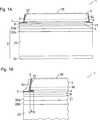
In
Beispielsweise
ist die aktive Schicht
An
einer der Strahlungsdurchtrittsfläche
Ferner
umfasst das Halbleiterbauteil
Zwischen
der Lotverbindungsschicht
Sowohl
der Träger
Bevorzugt
weist ein Material der Verkapselungsschicht
Die
Bestandteile des Halbleiterbauteils können, einzeln oder
in Kombination, wie nachfolgend angegeben geformt sein. Eine Dicke
der Halbleiterschichtenfolge
Eine
Dicke der zweiten Spiegelschicht
Das
Halbleiterbauteil
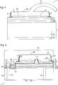
Auf
einem nicht gezeichneten Aufwachssubstrat wird die Halbleiterschichtenfolge
On a not shown growth substrate, the
Weiterhin
wird der Träger
Insbesondere
nach dem Entfernen des Aufwachssubstrats von der Halbleiterschichtenfolge
Vor
oder auch nach dem Erzeugen der Strukturierung an der Strahlungsdurchtrittsfläche
Ein
lateraler Überstand L der Halbleiterschichtenfolge
Ferner
ist die Verkapselungsschicht
In
Im
Gegensatz zur durch ein Atomlagenabscheiden, kurz ALD, erzeugten
Verkapselungsschicht
Ferner
unterscheiden sich die durch ALD erstellte Verkapselungsschicht
Beim
Ausführungsbeispiel gemäß
In
Gemäß dem
Ausführungsbeispiel nach
Beim
Ausführungsbeispiel gemäß
Wie
auch bei allen anderen Ausführungsbeispielen kann die Halbleiterschichtenfolge
Die hier beschriebene Erfindung ist nicht durch die Beschreibung anhand der Ausführungsbeispiele beschränkt. Vielmehr umfasst die Erfindung jedes neue Merkmal sowie jede Kombination von Merkmalen, was insbesondere jede Kombination von Merkmalen in den Patentansprüchen beinhaltet, auch wenn dieses Merkmal oder diese Kombination selbst nicht explizit in den Patentansprüchen oder Ausführungsbeispielen angegeben ist.The The invention described herein is not by the description limited to the embodiments. Much more For example, the invention includes every novel feature as well as every combination of features, in particular any combination of features in the patent claims, even if this feature or this combination itself is not explicitly stated in the claims or embodiments is given.
ZITATE ENTHALTEN IN DER BESCHREIBUNGQUOTES INCLUDE IN THE DESCRIPTION
Diese Liste der vom Anmelder aufgeführten Dokumente wurde automatisiert erzeugt und ist ausschließlich zur besseren Information des Lesers aufgenommen. Die Liste ist nicht Bestandteil der deutschen Patent- bzw. Gebrauchsmusteranmeldung. Das DPMA übernimmt keinerlei Haftung für etwaige Fehler oder Auslassungen.This list The documents listed by the applicant have been automated generated and is solely for better information recorded by the reader. The list is not part of the German Patent or utility model application. The DPMA takes over no liability for any errors or omissions.
Zitierte PatentliteraturCited patent literature
- - DE 102007004304 A1 [0003] DE 102007004304 A1 [0003]
- - US 4058430 A [0031] - US 4058430 A [0031]
Claims (15)
Priority Applications (8)
| Application Number | Priority Date | Filing Date | Title |
|---|---|---|---|
| DE102009033686A DE102009033686A1 (en) | 2009-07-17 | 2009-07-17 | Optoelectronic semiconductor component and method for producing an inorganic optoelectronic semiconductor component |
| JP2012519952A JP5755646B2 (en) | 2009-07-17 | 2010-06-10 | Optoelectronic semiconductor component and method of manufacturing inorganic optoelectronic semiconductor component |
| PCT/EP2010/058160 WO2011006719A1 (en) | 2009-07-17 | 2010-06-10 | Optoelectronic semiconductor component and method for producing an inorganic optoelectronic semiconductor component |
| KR1020127004141A KR101614106B1 (en) | 2009-07-17 | 2010-06-10 | Optoelectronic semiconductor component and method for producing an inorganic optoelectronic semiconductor component |
| US13/318,800 US8698178B2 (en) | 2009-07-17 | 2010-06-10 | Optoelectronic semiconductor component and method for producing an inorganic optoelectronic semiconductor component |
| CN201080029752.0A CN102473810B (en) | 2009-07-17 | 2010-06-10 | Opto-electronic semiconductor module and the method for the manufacture of the sub-semiconductor device of inorganic photovoltaic |
| EP10724846.0A EP2454763B1 (en) | 2009-07-17 | 2010-06-10 | Optoelectronic semiconductor component and method for producing an inorganic optoelectronic semiconductor component |
| TW099122953A TWI423486B (en) | 2009-07-17 | 2010-07-13 | Optoelectronic semiconductor component and method for producing an optoelectronic semiconductor component |
Applications Claiming Priority (1)
| Application Number | Priority Date | Filing Date | Title |
|---|---|---|---|
| DE102009033686A DE102009033686A1 (en) | 2009-07-17 | 2009-07-17 | Optoelectronic semiconductor component and method for producing an inorganic optoelectronic semiconductor component |
Publications (1)
| Publication Number | Publication Date |
|---|---|
| DE102009033686A1 true DE102009033686A1 (en) | 2011-01-20 |
Family
ID=42671937
Family Applications (1)
| Application Number | Title | Priority Date | Filing Date |
|---|---|---|---|
| DE102009033686A Withdrawn DE102009033686A1 (en) | 2009-07-17 | 2009-07-17 | Optoelectronic semiconductor component and method for producing an inorganic optoelectronic semiconductor component |
Country Status (8)
| Country | Link |
|---|---|
| US (1) | US8698178B2 (en) |
| EP (1) | EP2454763B1 (en) |
| JP (1) | JP5755646B2 (en) |
| KR (1) | KR101614106B1 (en) |
| CN (1) | CN102473810B (en) |
| DE (1) | DE102009033686A1 (en) |
| TW (1) | TWI423486B (en) |
| WO (1) | WO2011006719A1 (en) |
Cited By (13)
| Publication number | Priority date | Publication date | Assignee | Title |
|---|---|---|---|---|
| WO2012107290A1 (en) * | 2011-02-07 | 2012-08-16 | Osram Opto Semiconductors Gmbh | Optoelectronic semi-conductor chip with encapsulated mirror layer |
| DE102011011140A1 (en) * | 2011-02-14 | 2012-08-16 | Osram Opto Semiconductors Gmbh | Optoelectronic semiconductor chip and method for producing optoelectronic semiconductor chips |
| WO2012107289A1 (en) * | 2011-02-07 | 2012-08-16 | Osram Opto Semiconductors Gmbh | Optoelectronic semi-conductor chip with an encapsulated mirror layer |
| DE102011016302A1 (en) * | 2011-04-07 | 2012-10-11 | Osram Opto Semiconductors Gmbh | Optoelectronic semiconductor chip |
| EP2513984A1 (en) * | 2009-12-18 | 2012-10-24 | OSRAM Opto Semiconductors GmbH | Optoelectronic component and method for producing an opto-electronic component |
| DE102011112000A1 (en) * | 2011-08-31 | 2013-02-28 | Osram Opto Semiconductors Gmbh | LED chip |
| DE102012108879A1 (en) * | 2012-09-20 | 2014-03-20 | Osram Opto Semiconductors Gmbh | Optoelectronic semiconductor chip with a plurality of active regions arranged next to one another |
| WO2014114524A1 (en) * | 2013-01-28 | 2014-07-31 | Osram Opto Semiconductors Gmbh | Optoelectronic semiconductor chip encapsulated with an ald layer and corresponding method for production |
| US8872209B2 (en) | 2010-03-01 | 2014-10-28 | Osram Opto Semiconductors Gmbh | Light emitting diode chip |
| DE102013107531A1 (en) * | 2013-07-16 | 2015-01-22 | Osram Opto Semiconductors Gmbh | Optoelectronic semiconductor chip |
| WO2016023807A1 (en) * | 2014-08-12 | 2016-02-18 | Osram Opto Semiconductors Gmbh | Optoelectronic semiconductor chip and method for producing same |
| DE102015112280A1 (en) * | 2015-07-28 | 2017-02-02 | Osram Opto Semiconductors Gmbh | Component with a metallic carrier and method for the production of components |
| WO2017158113A1 (en) * | 2016-03-18 | 2017-09-21 | Osram Opto Semiconductors Gmbh | Method for producing an optoelectronic semiconductor chip and optoelectronic semiconductor chip |
Families Citing this family (16)
| Publication number | Priority date | Publication date | Assignee | Title |
|---|---|---|---|---|
| WO2012035135A1 (en) | 2010-09-19 | 2012-03-22 | Osram Opto Semiconductors Gmbh | Semiconductor chip and method for producing the same |
| WO2012141031A1 (en) * | 2011-04-11 | 2012-10-18 | 日亜化学工業株式会社 | Semiconductor light emitting element and method for manufacturing same |
| TWI488337B (en) * | 2011-07-12 | 2015-06-11 | Huga Optotech Inc | Light-emitting device and fabrication method thereof |
| TWI548118B (en) * | 2011-07-12 | 2016-09-01 | 廣鎵光電股份有限公司 | Light-emitting device and fabrication method thereof |
| US9620478B2 (en) | 2011-11-18 | 2017-04-11 | Apple Inc. | Method of fabricating a micro device transfer head |
| US8349116B1 (en) | 2011-11-18 | 2013-01-08 | LuxVue Technology Corporation | Micro device transfer head heater assembly and method of transferring a micro device |
| US8794501B2 (en) * | 2011-11-18 | 2014-08-05 | LuxVue Technology Corporation | Method of transferring a light emitting diode |
| US8573469B2 (en) | 2011-11-18 | 2013-11-05 | LuxVue Technology Corporation | Method of forming a micro LED structure and array of micro LED structures with an electrically insulating layer |
| DE102012101889A1 (en) | 2012-03-06 | 2013-09-12 | Osram Opto Semiconductors Gmbh | Method for producing an optoelectronic semiconductor chip and optoelectronic semiconductor chip |
| JP6135213B2 (en) * | 2012-04-18 | 2017-05-31 | 日亜化学工業株式会社 | Semiconductor light emitting device |
| DE102013107967B4 (en) * | 2013-07-25 | 2021-05-06 | OSRAM Opto Semiconductors Gesellschaft mit beschränkter Haftung | Optoelectronic semiconductor chip, optoelectronic component and method for producing a plurality of optoelectronic semiconductor chips |
| CN104659165B (en) * | 2015-02-11 | 2018-09-25 | 山东浪潮华光光电子股份有限公司 | A kind of preparation method of GaN base light emitting chip |
| DE102015118041A1 (en) | 2015-10-22 | 2017-04-27 | Osram Opto Semiconductors Gmbh | Light-emitting diode chip and method for producing a light-emitting diode chip |
| DE102016106928A1 (en) * | 2016-04-14 | 2017-10-19 | Osram Opto Semiconductors Gmbh | Optoelectronic semiconductor chip and method for producing an optoelectronic semiconductor chip |
| US11799058B2 (en) | 2018-03-15 | 2023-10-24 | Osram Oled Gmbh | Optoelectronic semiconductor chip |
| DE102018107673A1 (en) | 2018-03-15 | 2019-09-19 | Osram Opto Semiconductors Gmbh | Optoelectronic semiconductor chip and production method for an optoelectronic semiconductor chip |
Citations (5)
| Publication number | Priority date | Publication date | Assignee | Title |
|---|---|---|---|---|
| US4058430A (en) | 1974-11-29 | 1977-11-15 | Tuomo Suntola | Method for producing compound thin films |
| DE102007004304A1 (en) | 2007-01-29 | 2008-07-31 | Osram Opto Semiconductors Gmbh | Thin-film light emitting diode chip, has layer stack made of primary radiation surfaces lying opposite to each other so that thin-film light emitting diode chip has two primary radiation directions |
| DE102007022947A1 (en) * | 2007-04-26 | 2008-10-30 | Osram Opto Semiconductors Gmbh | Optoelectronic semiconductor body and method for producing such |
| US7622746B1 (en) * | 2006-03-17 | 2009-11-24 | Bridgelux, Inc. | Highly reflective mounting arrangement for LEDs |
| US20100008391A1 (en) * | 2008-03-05 | 2010-01-14 | Rohm Co., Ltd. | Nitride based semiconductor device and fabrication method for the same |
Family Cites Families (20)
| Publication number | Priority date | Publication date | Assignee | Title |
|---|---|---|---|---|
| JPH05235406A (en) * | 1992-02-26 | 1993-09-10 | Kyocera Corp | Semiconductor light-emitting device |
| AU2003207287B2 (en) | 2002-01-28 | 2007-12-13 | Nichia Corporation | Nitride semiconductor device having support substrate and its manufacturing method |
| US6841802B2 (en) * | 2002-06-26 | 2005-01-11 | Oriol, Inc. | Thin film light emitting diode |
| JP4165227B2 (en) | 2003-01-07 | 2008-10-15 | 株式会社デンソー | Organic EL display device |
| JP4325232B2 (en) * | 2003-03-18 | 2009-09-02 | 日亜化学工業株式会社 | Nitride semiconductor device |
| FR2861386B1 (en) * | 2003-10-23 | 2006-02-17 | Saint Gobain | SUBSTRATE, IN PARTICULAR GLASS SUBSTRATE, CARRYING A PHOTOCATALYTIC LAYER COATED WITH A PROTECTIVE THIN LAYER. |
| US8174037B2 (en) * | 2004-09-22 | 2012-05-08 | Cree, Inc. | High efficiency group III nitride LED with lenticular surface |
| JP2006100500A (en) * | 2004-09-29 | 2006-04-13 | Sanken Electric Co Ltd | Semiconductor light emitting device and its manufacturing method |
| JP5016808B2 (en) * | 2005-11-08 | 2012-09-05 | ローム株式会社 | Nitride semiconductor light emitting device and method for manufacturing nitride semiconductor light emitting device |
| KR100640496B1 (en) | 2005-11-23 | 2006-11-01 | 삼성전기주식회사 | Vertically structured gan type led device |
| JP2007273590A (en) * | 2006-03-30 | 2007-10-18 | Rohm Co Ltd | Nitride semiconductor element and its manufacturing method |
| JP4203087B2 (en) * | 2006-07-25 | 2008-12-24 | 株式会社沖データ | Semiconductor composite device, LED print head, and image forming apparatus |
| US20080087875A1 (en) | 2006-10-11 | 2008-04-17 | Feng-Hsu Fan | Protection for the epitaxial structure of metal devices |
| KR101329908B1 (en) * | 2006-10-13 | 2013-11-14 | 퓨처 라이트 리미티드 라이어빌러티 컴퍼니 | Semiconductor light-emitting device, illuminator and method of manufacturing semiconductor light-emitting device |
| KR100867541B1 (en) * | 2006-11-14 | 2008-11-06 | 삼성전기주식회사 | Method of manufacturing vertical light emitting device |
| DE102007029370A1 (en) | 2007-05-04 | 2008-11-06 | Osram Opto Semiconductors Gmbh | Semiconductor chip and method for producing a semiconductor chip |
| JP4879094B2 (en) * | 2007-06-06 | 2012-02-15 | 浜松ホトニクス株式会社 | Semiconductor light emitting device and manufacturing method thereof |
| KR101371511B1 (en) | 2007-10-04 | 2014-03-11 | 엘지이노텍 주식회사 | Light emitting device having vertical topology |
| US8314446B2 (en) * | 2007-10-11 | 2012-11-20 | Wavefront Holdings, Llc | Photo-detector array, semiconductor image intensifier and methods of making and using the same |
| EP2234182B1 (en) * | 2007-12-28 | 2016-11-09 | Nichia Corporation | Semiconductor light emitting element and method for manufacturing the same |
-
2009
- 2009-07-17 DE DE102009033686A patent/DE102009033686A1/en not_active Withdrawn
-
2010
- 2010-06-10 KR KR1020127004141A patent/KR101614106B1/en active IP Right Grant
- 2010-06-10 CN CN201080029752.0A patent/CN102473810B/en not_active Expired - Fee Related
- 2010-06-10 US US13/318,800 patent/US8698178B2/en active Active
- 2010-06-10 WO PCT/EP2010/058160 patent/WO2011006719A1/en active Application Filing
- 2010-06-10 EP EP10724846.0A patent/EP2454763B1/en not_active Not-in-force
- 2010-06-10 JP JP2012519952A patent/JP5755646B2/en not_active Expired - Fee Related
- 2010-07-13 TW TW099122953A patent/TWI423486B/en not_active IP Right Cessation
Patent Citations (5)
| Publication number | Priority date | Publication date | Assignee | Title |
|---|---|---|---|---|
| US4058430A (en) | 1974-11-29 | 1977-11-15 | Tuomo Suntola | Method for producing compound thin films |
| US7622746B1 (en) * | 2006-03-17 | 2009-11-24 | Bridgelux, Inc. | Highly reflective mounting arrangement for LEDs |
| DE102007004304A1 (en) | 2007-01-29 | 2008-07-31 | Osram Opto Semiconductors Gmbh | Thin-film light emitting diode chip, has layer stack made of primary radiation surfaces lying opposite to each other so that thin-film light emitting diode chip has two primary radiation directions |
| DE102007022947A1 (en) * | 2007-04-26 | 2008-10-30 | Osram Opto Semiconductors Gmbh | Optoelectronic semiconductor body and method for producing such |
| US20100008391A1 (en) * | 2008-03-05 | 2010-01-14 | Rohm Co., Ltd. | Nitride based semiconductor device and fabrication method for the same |
Cited By (30)
| Publication number | Priority date | Publication date | Assignee | Title |
|---|---|---|---|---|
| US9768360B2 (en) | 2009-12-18 | 2017-09-19 | Osram Opto Semiconductors Gmbh | Optoelectronic component and method of producing an optoelectronic component |
| US9508903B2 (en) | 2009-12-18 | 2016-11-29 | Osram Opto Semiconductors Gmbh | Optoelectronic component and method for producing an optoelectronic component |
| EP2513984A1 (en) * | 2009-12-18 | 2012-10-24 | OSRAM Opto Semiconductors GmbH | Optoelectronic component and method for producing an opto-electronic component |
| US8872209B2 (en) | 2010-03-01 | 2014-10-28 | Osram Opto Semiconductors Gmbh | Light emitting diode chip |
| WO2012107289A1 (en) * | 2011-02-07 | 2012-08-16 | Osram Opto Semiconductors Gmbh | Optoelectronic semi-conductor chip with an encapsulated mirror layer |
| WO2012107290A1 (en) * | 2011-02-07 | 2012-08-16 | Osram Opto Semiconductors Gmbh | Optoelectronic semi-conductor chip with encapsulated mirror layer |
| CN103384923B (en) * | 2011-02-14 | 2016-06-15 | 欧司朗光电半导体有限公司 | Opto-electronic semiconductor chip and the method for manufacturing opto-electronic semiconductor chip |
| US9722136B2 (en) | 2011-02-14 | 2017-08-01 | Osram Opto Semiconductors Gmbh | Optoelectronic semiconductor chip and method for producing optoelectronic semiconductor chips |
| CN103384923A (en) * | 2011-02-14 | 2013-11-06 | 欧司朗光电半导体有限公司 | Optoelectronic semiconductor chip and method for producing optoelectronic semiconductor chips |
| US10164143B2 (en) | 2011-02-14 | 2018-12-25 | Osram Opto Semiconductors Gmbh | Optoelectronic semiconductor chip and method for producing optoelectronic semiconductor chips |
| DE102011011140A1 (en) * | 2011-02-14 | 2012-08-16 | Osram Opto Semiconductors Gmbh | Optoelectronic semiconductor chip and method for producing optoelectronic semiconductor chips |
| US9343637B2 (en) | 2011-02-14 | 2016-05-17 | Osram Opto Semiconductors Gmbh | Optoelectronic semiconductor chip and method for producing optoelectronic semiconductor chips |
| DE102011016302A1 (en) * | 2011-04-07 | 2012-10-11 | Osram Opto Semiconductors Gmbh | Optoelectronic semiconductor chip |
| US9741912B2 (en) | 2011-04-07 | 2017-08-22 | Osram Opto Semiconductors Gmbh | Optoelectronic semiconductor chip |
| DE102011112000B4 (en) | 2011-08-31 | 2023-11-30 | OSRAM Opto Semiconductors Gesellschaft mit beschränkter Haftung | LED chip |
| US10043958B2 (en) | 2011-08-31 | 2018-08-07 | Osram Opto Semiconductors Gmbh | Light emitting diode chip |
| DE102011112000A1 (en) * | 2011-08-31 | 2013-02-28 | Osram Opto Semiconductors Gmbh | LED chip |
| US9577165B2 (en) | 2011-08-31 | 2017-02-21 | Osram Opto Semiconductor Gmbh | Light emitting diode chip |
| US9299897B2 (en) | 2012-09-20 | 2016-03-29 | Osram Opto Semiconductors Gmbh | Optoelectronic semiconductor chip having a plurality of active regions arranged alongside one another |
| DE102012108879A1 (en) * | 2012-09-20 | 2014-03-20 | Osram Opto Semiconductors Gmbh | Optoelectronic semiconductor chip with a plurality of active regions arranged next to one another |
| DE102012108879B4 (en) | 2012-09-20 | 2024-03-28 | OSRAM Opto Semiconductors Gesellschaft mit beschränkter Haftung | Optoelectronic semiconductor chip with several active areas arranged next to one another |
| US9761770B2 (en) | 2013-01-28 | 2017-09-12 | Osram Opto Semiconductors Gmbh | Optoelectronic semiconductor chip encapsulated with an ALD layer and corresponding method for production |
| WO2014114524A1 (en) * | 2013-01-28 | 2014-07-31 | Osram Opto Semiconductors Gmbh | Optoelectronic semiconductor chip encapsulated with an ald layer and corresponding method for production |
| US10014444B2 (en) | 2013-07-16 | 2018-07-03 | Osram Opto Semiconductors Gmbh | Optoelectronic semiconductor chip |
| DE102013107531A1 (en) * | 2013-07-16 | 2015-01-22 | Osram Opto Semiconductors Gmbh | Optoelectronic semiconductor chip |
| WO2016023807A1 (en) * | 2014-08-12 | 2016-02-18 | Osram Opto Semiconductors Gmbh | Optoelectronic semiconductor chip and method for producing same |
| DE102015112280A1 (en) * | 2015-07-28 | 2017-02-02 | Osram Opto Semiconductors Gmbh | Component with a metallic carrier and method for the production of components |
| US10665758B2 (en) | 2015-07-28 | 2020-05-26 | Osram Oled Gmbh | Component having a metal carrier and method for producing components |
| WO2017158113A1 (en) * | 2016-03-18 | 2017-09-21 | Osram Opto Semiconductors Gmbh | Method for producing an optoelectronic semiconductor chip and optoelectronic semiconductor chip |
| US10658548B2 (en) | 2016-03-18 | 2020-05-19 | Osram Oled Gmbh | Method for producing an optoelectronic semiconductor chip and optoelectronic semiconductor chip |
Also Published As
| Publication number | Publication date |
|---|---|
| CN102473810A (en) | 2012-05-23 |
| TW201115793A (en) | 2011-05-01 |
| KR20120052327A (en) | 2012-05-23 |
| JP2012533873A (en) | 2012-12-27 |
| TWI423486B (en) | 2014-01-11 |
| CN102473810B (en) | 2015-09-23 |
| US8698178B2 (en) | 2014-04-15 |
| EP2454763B1 (en) | 2017-01-18 |
| EP2454763A1 (en) | 2012-05-23 |
| US20120098016A1 (en) | 2012-04-26 |
| JP5755646B2 (en) | 2015-07-29 |
| WO2011006719A1 (en) | 2011-01-20 |
| KR101614106B1 (en) | 2016-04-20 |
Similar Documents
| Publication | Publication Date | Title |
|---|---|---|
| DE102009033686A1 (en) | Optoelectronic semiconductor component and method for producing an inorganic optoelectronic semiconductor component | |
| DE102007029370A1 (en) | Semiconductor chip and method for producing a semiconductor chip | |
| DE102011016302A1 (en) | Optoelectronic semiconductor chip | |
| DE102010024079A1 (en) | Method for producing an optoelectronic semiconductor chip and optoelectronic semiconductor chip | |
| DE102007004302A1 (en) | Semiconductor chip for light emitting diode, has support with two support surfaces, and semiconductor layer sequence has active area for generation of radiation | |
| DE102010034665A1 (en) | Optoelectronic semiconductor chip and method for producing optoelectronic semiconductor chips | |
| DE102012108879B4 (en) | Optoelectronic semiconductor chip with several active areas arranged next to one another | |
| WO2012110364A1 (en) | Optoelectronic semiconductor chip and method for producing optoelectronic semiconductor chips | |
| DE102015118041A1 (en) | Light-emitting diode chip and method for producing a light-emitting diode chip | |
| WO2012013523A1 (en) | Radation-emitting semi-conductor chip and a method for producing a radiation-emitting semi-conductor chip | |
| DE102018107673A1 (en) | Optoelectronic semiconductor chip and production method for an optoelectronic semiconductor chip | |
| DE102015120323A1 (en) | LED chip with a reflective layer sequence | |
| DE102011010503A1 (en) | Optoelectronic semiconductor chip | |
| WO2015177164A1 (en) | Method for producing an optoelectronic semiconductor chip, and an optoelectronic semiconductor chip | |
| DE102008028886A1 (en) | Radiation-emitting component and method for producing a radiation-emitting component | |
| WO2018114807A1 (en) | Optoelectronic semiconductor chip and method for producing an optoelectronic semiconductor chip | |
| DE102011010504A1 (en) | Optoelectric semiconductor chip | |
| DE102011017097A1 (en) | Method for producing a semiconductor body | |
| DE102011115299A1 (en) | Optoelectronic semiconductor chip and method for producing an optoelectronic semiconductor chip | |
| WO2016066477A1 (en) | Optoelectronic semiconductor chip | |
| DE102013113106A1 (en) | Radiation emitting semiconductor chip | |
| DE102012110775A1 (en) | Optoelectronic semiconductor chip and method for producing an optoelectronic semiconductor chip | |
| DE102014107306A1 (en) | Method for producing an optoelectronic semiconductor chip and optoelectronic semiconductor chip | |
| DE102017117414A1 (en) | Method for producing an optoelectronic component and optoelectronic component | |
| WO2021043901A1 (en) | Optoelectronic component and method for manufacturing an optoelectronic component |
Legal Events
| Date | Code | Title | Description |
|---|---|---|---|
| OM8 | Search report available as to paragraph 43 lit. 1 sentence 1 patent law | ||
| R005 | Application deemed withdrawn due to failure to request examination |