CN217717334U - PCB circuit board bending force detection device - Google Patents
PCB circuit board bending force detection device Download PDFInfo
- Publication number
- CN217717334U CN217717334U CN202221613368.1U CN202221613368U CN217717334U CN 217717334 U CN217717334 U CN 217717334U CN 202221613368 U CN202221613368 U CN 202221613368U CN 217717334 U CN217717334 U CN 217717334U
- Authority
- CN
- China
- Prior art keywords
- detection device
- pcb
- bending force
- force detection
- telescopic cylinder
- Prior art date
- Legal status (The legal status is an assumption and is not a legal conclusion. Google has not performed a legal analysis and makes no representation as to the accuracy of the status listed.)
- Active
Links
Images


Landscapes
- Force Measurement Appropriate To Specific Purposes (AREA)
Abstract
The utility model discloses a PCB circuit board bending force detection device, which comprises an operation table and a bending force detection device, wherein the bending force detection device is arranged on the operation table, the bending force detection device comprises a clamping structure, a pressing structure and a supporting structure, the clamping structure is arranged on the operation table, the pressing structure is arranged on the operation table, the supporting structure is arranged on the operation table, and the clamping structure comprises a telescopic cylinder, a connecting rod, a pressing plate, a positioning block, a buffer plate and a spring; the utility model discloses be provided with and press from both sides tight structure, press from both sides tight structure and include telescopic cylinder, connecting rod, pressure strip, locating piece, buffer board and spring, through the cooperation between each part of the tight structure of clamp, can press from both sides tight location to PCB board one end, avoid causing the fish tail to the PCB board surface, guarantee the quality of PCB board; the scheme is provided with a pressure applying structure and a supporting structure, and the PCB is pressed through the matching of all parts of the pressure applying structure.
Description
Technical Field
The utility model relates to a PCB circuit board technical field specifically is a PCB circuit board power detection device of buckling.
Background
The PCB circuit board generally refers to a printed circuit board, also called a printed circuit board, which is an important electronic component, is a support body of an electronic component and a carrier for electrical connection of the electronic component, and needs to be subjected to bending force detection in the production process of the PCB circuit board so as to detect whether the bending resistance of the PCB board is qualified or not;
1. when the traditional PCB circuit board is subjected to bending force detection, the PCB board needs to be clamped and positioned, and the surface of the circuit board is easily scratched in the clamping process, so that the scratch on the surface of the circuit board is caused, and the quality of the circuit board is affected.
2. When the bending force of a traditional PCB is detected, the bending force of different positions of the same PCB cannot be detected, so that the measurement data is single, and the measurement result is not accurate enough.
SUMMERY OF THE UTILITY MODEL
In order to achieve the above purpose, the utility model discloses a following technical scheme realizes: a PCB (printed circuit board) bending force detection device comprises an operation table and a bending force detection device, wherein the bending force detection device is installed on the operation table and comprises a clamping structure, a pressing structure and a supporting structure, the clamping structure is installed on the operation table, the pressing structure is installed on the operation table, the supporting structure is installed on the operation table, and the clamping structure comprises a telescopic cylinder, a connecting rod, a pressing plate, a positioning block, a buffer plate and a spring;
the locating piece is installed on the operation panel, and spring mounting is on the locating piece, and the buffer board is installed on the locating piece, and telescopic cylinder installs on the locating piece, and the connecting rod is installed on telescopic cylinder, and the pressure strip is installed on the connecting rod.
Preferably, the positioning block is provided with a limiting groove and a limiting hole.
Preferably, the pressure applying structure comprises a support frame, a linear electric guide rail, a telescopic cylinder, a pressure plate, a pressure sensor and a controller;
the support frame is installed on the operation panel, and sharp electric rail installs on the support frame, and telescopic cylinder installs at sharp electric rail drive end, and the flexible end at telescopic cylinder is installed to the clamp plate, and pressure sensor installs on the clamp plate, and the controller is installed on the support frame.
Preferably, the pressure plate is provided with a positioning groove.
Preferably, the support frame is provided with a display screen.
Preferably, the supporting structure comprises a limiting block, a threaded lead screw, a sliding block, a supporting block, a guide rod and a hand-operated wheel;
the stopper is installed on the operation panel, and the screw lead screw is installed on the stopper, and the slider is installed on the screw lead screw, and the guide bar is installed on the stopper and is inlayed and install on the slider, and hand wheel is installed on the screw lead screw.
Advantageous effects
The utility model provides a PCB circuit board bending force detection device possesses following beneficial effect:
1. the clamping structure is arranged, and one end of the PCB can be clamped and positioned through the matching of all parts of the clamping structure, so that the surface of the PCB is prevented from being scratched, and the quality of the PCB is ensured;
2. be provided with structure and the bearing structure of exerting pressure, exert pressure to the PCB board through the cooperation between each part of the structure of exerting pressure, carry out the auxiliary stay to the PCB board through the cooperation between each part of bearing structure, bearing structure can change the support position to the PCB board, and the adjustment structure of exerting pressure can carry out the bending force to detect the different positions of PCB board to the position of exerting pressure of PCB board, guarantees the accuracy to the measuring result of PCB board.
Drawings
Fig. 1 is a schematic three-dimensional structure diagram of a PCB circuit board bending force detection device of the present invention;
fig. 2 is a schematic view of a front view structure of the PCB circuit board bending force detecting device of the present invention;
fig. 3 is a left side view structural diagram of the PCB circuit board bending force detecting device of the present invention;
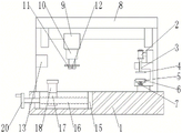
in the figure: 1. an operation table; 2. a telescopic cylinder; 3. a connecting rod; 4. a compression plate; 5. positioning a block; 6. A buffer plate; 7. a spring; 8. a support frame; 9. a linear electric guide rail; 10. a telescopic cylinder; 11. pressing a plate; 12. a pressure sensor; 13. a controller; 14. a display screen; 15. a limiting block; 16. a threaded lead screw; 17. a slider; 18. a support block; 19. a guide bar; 20. a hand-operated wheel;
Detailed Description
Based on the embodiments in the present invention, all other embodiments obtained by a person skilled in the art without creative work belong to the protection scope of the present invention.
Referring to fig. 1-3, the present invention provides a PCB circuit board bending force detecting device.
The embodiment is as follows:
referring to fig. 1-3, in a specific implementation process, a PCB circuit board bending force detection device includes an operation table 1 and a bending force detection device, the bending force detection device is installed on the operation table 1, the bending force detection device includes a clamping structure, a pressure applying structure and a supporting structure, the clamping structure is installed on the operation table 1, the pressure applying structure is installed on the operation table 1, the supporting structure is installed on the operation table 1, and the clamping structure includes a telescopic cylinder 10, a connecting rod 3, a pressure applying plate 4, a positioning block 5, a buffer plate 6 and a spring 7;
the positioning block 5 is installed on the operating table 1, the spring 7 is installed on the positioning block 5, the buffer plate 6 is installed on the positioning block 5, the telescopic cylinder 10 is installed on the positioning block 5, the connecting rod 3 is installed on the telescopic cylinder 10, and the pressing plate 4 is installed on the connecting rod 3;
the PCB is placed on the operation table 1, the bending force detection is performed after the PCB is positioned through the bending force detection device, the bending force detection device comprises a clamping structure, a pressing structure and a supporting structure, one end of the PCB can be clamped and positioned through the matching of all parts of the clamping structure, scratch on the surface of the PCB is avoided, the quality of the PCB is guaranteed, the PCB is stably pressed through the matching of all parts of the pressing structure, when the applied pressure reaches a specified value, the deformation degree of the PCB is checked to check whether the PCB is qualified or not, the PCB is supported in an auxiliary mode through the matching of all parts of the supporting structure, the supporting position of the PCB can be changed through the supporting structure, the pressing position of the pressing structure on the PCB can be adjusted, the bending force detection can be performed on different positions of the PCB, and the accuracy of the measurement result of the PCB is guaranteed;
locating piece 5 is the type of falling U structrual installation on operation panel 1, place the PCB board between locating piece 5, start telescopic cylinder 10, telescopic cylinder 10 drives connecting rod 3 downstream, pressure strip 4 installs on connecting rod 3, when pressure strip 4 downstream under the drive of connecting rod 3, promote PCB board contact buffer board 6, buffer board 6 extrusion spring 7, under spring 7's effect, cushion the PCB board, avoid pressure strip 4's impact force too big to cause the damage to the PCB board, after buffer board 6 sinks locating piece 5 completely, the PCB board falls on locating piece 5, through the cooperation of pressure strip 4 to locating piece 5, press from both sides tightly the PCB board.
In the specific implementation process, the positioning block 5 is provided with a limiting groove and a limiting hole;
it should be noted that the limiting groove is convenient for the buffer plate 6 to completely sink into the positioning block 5, the limiting hole is convenient for the installation of the connecting rod 3, and the connecting rod 3 is guided through the limiting hole.
In the specific implementation process, the pressure applying structure comprises a support frame 8, a linear electric guide rail 9, a telescopic cylinder 10, a pressure plate 11, a pressure sensor 12 and a controller 13;
the support frame 8 is installed on the operating platform 1, the linear electric guide rail 9 is installed on the support frame 8, the telescopic cylinder 10 is installed at the driving end of the linear electric guide rail 9, the pressing plate 11 is installed at the telescopic end of the telescopic cylinder 10, the pressure sensor 12 is installed on the pressing plate 11, and the controller 13 is installed on the support frame 8;
it should be noted that, the linear electric guide rail 9 is installed on the operation table 1 through the support frame 8, the linear electric guide rail 9 drives the telescopic cylinder 10 to move, when the linear electric guide rail is moved to a position to be detected above the PCB, the pressing plate 11 is driven by the telescopic cylinder 10 to apply pressure to the PCB, the pressure sensor 12 transmits the sensed pressure to the controller 13 in the form of an electric signal, when the applied pressure reaches a specified pressure value, the controller 13 controls the telescopic cylinder 10 to stop working, the deformation degree of the PCB is observed, whether the PCB is qualified is detected, after the test is completed, the telescopic cylinder 10 is controlled to contract by the controller 13, the linear electric guide rail 9 is started, the telescopic cylinder 10 is driven to move to another point position to detect the bending force of the PCB, and the accuracy of the detection result is ensured.
In the specific implementation process, the pressure plate 11 is provided with a positioning groove;
it should be noted that the positioning groove on the pressure plate 11 facilitates the installation of the pressure sensor 12.
In a specific implementation process, the support frame 8 is provided with a display screen 14;
it should be noted that the pressure value is displayed on the display screen 14, so that the pressure change can be observed conveniently.
In the specific implementation process, the supporting structure comprises a limiting block 15, a threaded lead screw 16, a sliding block 17, a supporting block 18, a guide rod 19 and a hand wheel 20;
the limiting block 15 is installed on the operating table 1, the threaded lead screw 16 is installed on the limiting block 15, the sliding block 17 is installed on the threaded lead screw 16, the guide rod 19 is installed on the limiting block 15 and is embedded on the sliding block 17, and the hand-operated wheel 20 is installed on the threaded lead screw 16;
it should be noted that the hand wheel 20 drives the threaded lead screw 16 to rotate, a threaded sleeve is arranged in the slider 17, the slider 17 is mounted on the threaded lead screw 16 through the threaded sleeve, when the threaded lead screw 16 rotates, the slider 17 is driven to move along the direction of the guide rod 19, the supporting block 18 is mounted on the slider 17, the supporting block 18 moves along with the movement of the slider 17, the height of the upper surface of the supporting block 18 is the same as the height of the uppermost surface of the stepped surface of the limiting groove on the positioning block 5, so that the PCB can be stably supported, the PCB is prevented from being inclined, and the limiting block 15 supports the threaded lead screw 16 and the guide rod 19.
Although embodiments of the present invention have been shown and described, it will be appreciated by those skilled in the art that various changes, modifications, substitutions and alterations can be made in these embodiments without departing from the principles and spirit of the invention, the scope of which is defined in the appended claims and their equivalents.
Claims (6)
1. The utility model provides a PCB circuit board power detection device that buckles, includes the operation panel and buckles power detection device, buckles power detection device and installs on the operation panel, buckles power detection device including pressing from both sides tight structure, the structure and the bearing structure of exerting pressure, press from both sides tight structrual installation on the operation panel, the structrual installation that exerts pressure is on the operation panel, bearing structure installs on the operation panel, press from both sides tight structure and include telescopic cylinder, connecting rod, pressure strip, locating piece, buffer board and spring, its characterized in that:
the locating piece is installed on the operation panel, and spring mounting is on the locating piece, and the buffer board is installed on the locating piece, and telescopic cylinder installs on the locating piece, and the connecting rod is installed on telescopic cylinder, and the pressure strip is installed on the connecting rod.
2. The PCB circuit board bending force detection device of claim 1, wherein the positioning block is provided with a limiting groove and a limiting hole.
3. The PCB bending force detection device of claim 1, wherein the pressing structure comprises a support frame, a linear electric guide rail, a telescopic cylinder, a pressing plate, a pressure sensor and a controller;
the support frame is installed on the operation panel, and sharp electric rail installs on the support frame, and telescopic cylinder installs at sharp electric rail drive end, and the flexible end at telescopic cylinder is installed to the clamp plate, and pressure sensor installs on the clamp plate, and the controller is installed on the support frame.
4. The PCB bending force detection device of claim 3, wherein the pressing plate is provided with a positioning groove.
5. The PCB bending force detection device of claim 3, wherein a display screen is arranged on the support frame.
6. The PCB circuit board bending force detection device of claim 1, wherein the support structure comprises a limiting block, a threaded lead screw, a sliding block, a supporting block, a guide rod and a hand crank wheel;
the stopper is installed on the operation panel, and the screw lead screw is installed on the stopper, and the slider is installed on the screw lead screw, and the guide bar is installed on the stopper and is inlayed and install on the slider, and hand wheel is installed on the screw lead screw.
Priority Applications (1)
| Application Number | Priority Date | Filing Date | Title |
|---|---|---|---|
| CN202221613368.1U CN217717334U (en) | 2022-06-27 | 2022-06-27 | PCB circuit board bending force detection device |
Applications Claiming Priority (1)
| Application Number | Priority Date | Filing Date | Title |
|---|---|---|---|
| CN202221613368.1U CN217717334U (en) | 2022-06-27 | 2022-06-27 | PCB circuit board bending force detection device |
Publications (1)
| Publication Number | Publication Date |
|---|---|
| CN217717334U true CN217717334U (en) | 2022-11-01 |
Family
ID=83775647
Family Applications (1)
| Application Number | Title | Priority Date | Filing Date |
|---|---|---|---|
| CN202221613368.1U Active CN217717334U (en) | 2022-06-27 | 2022-06-27 | PCB circuit board bending force detection device |
Country Status (1)
| Country | Link |
|---|---|
| CN (1) | CN217717334U (en) |
Cited By (2)
| Publication number | Priority date | Publication date | Assignee | Title |
|---|---|---|---|---|
| CN116754391A (en) * | 2023-08-08 | 2023-09-15 | 常州市佳瑞精密机械有限公司 | Pressure testing device and method for saliva suction tube production |
| CN117782848A (en) * | 2024-02-23 | 2024-03-29 | 梨树全创科技有限公司 | Circuit board bending performance testing device and testing method thereof |
-
2022
- 2022-06-27 CN CN202221613368.1U patent/CN217717334U/en active Active
Cited By (4)
| Publication number | Priority date | Publication date | Assignee | Title |
|---|---|---|---|---|
| CN116754391A (en) * | 2023-08-08 | 2023-09-15 | 常州市佳瑞精密机械有限公司 | Pressure testing device and method for saliva suction tube production |
| CN116754391B (en) * | 2023-08-08 | 2023-11-03 | 常州市佳瑞精密机械有限公司 | Pressure testing device and method for saliva suction tube production |
| CN117782848A (en) * | 2024-02-23 | 2024-03-29 | 梨树全创科技有限公司 | Circuit board bending performance testing device and testing method thereof |
| CN117782848B (en) * | 2024-02-23 | 2024-05-14 | 梨树全创科技有限公司 | Circuit board bending performance testing device and testing method thereof |
Similar Documents
| Publication | Publication Date | Title |
|---|---|---|
| CN217717334U (en) | PCB circuit board bending force detection device | |
| CN103458671B (en) | A kind of contraposition kludge | |
| CN211121107U (en) | Flatness measuring instrument | |
| CN217210749U (en) | Riveting detection and discharge device for silencer | |
| CN215179332U (en) | A testing arrangement for fastener hardness | |
| CN213021356U (en) | Novel contact height detection machine | |
| CN203416570U (en) | Alignment assembly machine | |
| CN105180881A (en) | Parallelism detection device | |
| CN104316868A (en) | Testing device for dynamic characteristic of contactor | |
| CN109186423B (en) | Nondestructive precision measurement equipment and precision measurement method for angle of mechanical part | |
| CN105108295A (en) | Online control press-connection machine | |
| CN210072259U (en) | LCD glass automatic testing machine | |
| CN214503709U (en) | Test probe station capable of mounting various probe cards | |
| CN212275457U (en) | Tensile sample shoulder length center positioning device | |
| CN211147630U (en) | Inner hole roughness automatic detection machine | |
| CN212146051U (en) | Positioning mechanism for quick detection of resilience precision of plane bent pipe | |
| CN112847291A (en) | Gauge length marking device and using method thereof | |
| CN219016739U (en) | Positioning and clamping device of pressurizing jig | |
| CN211904603U (en) | Camera detection equipment clamping device | |
| CN218197433U (en) | Printing drive assembly of ultrathin circuit control board | |
| CN214666715U (en) | Thickness measuring device for circuit board | |
| CN111781065B (en) | Stretching sample shoulder opening length center positioning device | |
| CN213632030U (en) | Steel wire positioning detection device | |
| CN216925548U (en) | Measure equipment of concrete test block roughness | |
| CN212109950U (en) | Thickness difference detection tool |
Legal Events
| Date | Code | Title | Description |
|---|---|---|---|
| GR01 | Patent grant | ||
| GR01 | Patent grant |