CN210380944U - Electronic device - Google Patents
Electronic device Download PDFInfo
- Publication number
- CN210380944U CN210380944U CN201921691158.2U CN201921691158U CN210380944U CN 210380944 U CN210380944 U CN 210380944U CN 201921691158 U CN201921691158 U CN 201921691158U CN 210380944 U CN210380944 U CN 210380944U
- Authority
- CN
- China
- Prior art keywords
- electronic device
- display
- side body
- shielding member
- display area
- Prior art date
- Legal status (The legal status is an assumption and is not a legal conclusion. Google has not performed a legal analysis and makes no representation as to the accuracy of the status listed.)
- Active
Links
Images


Abstract
An embodiment of the present application provides an electronic device, including: the display screen comprises a main body part and a side body part, wherein the side body part is connected with the main body part, is bent towards one side of the main body part where a non-display surface is located, and comprises a non-display area; and the shielding piece is arranged on one side of the display surface of the side body part and is connected to the non-display area, so that the shielding piece shields the non-display area. The shielding piece is arranged on the side body part of the display screen, so that the shielding piece shields the non-display area, the black frame of the display screen can be shielded by the shielding piece, and the appearance effect of the electronic equipment can be improved.
Description
Technical Field
The present application relates to the field of electronic technologies, and in particular, to an electronic device.
Background
With the development of communication technology, electronic devices such as smart phones are becoming more and more popular. During the use process of the electronic equipment, the electronic equipment can display a picture by using the display device of the electronic equipment. However, the edge of a general display screen has a black frame, which affects the display effect of the display screen.
Disclosure of Invention
The embodiment of the application provides electronic equipment which can shield a non-display area at the edge of a display screen.
An embodiment of the present application provides an electronic device, including:
the display screen comprises a main body part and a side body part, wherein the side body part is connected with the main body part, is bent towards one side of the main body part where a non-display surface is located, and comprises a non-display area; and
and the shielding piece is arranged on one side of the display surface of the side body part and is connected to the non-display area so as to shield the non-display area.
The electronic equipment that this application embodiment provided sets up the shielding piece through the side body portion at the display screen, makes the shielding piece correspond the setting with the non-display area of side body portion to can realize that the shielding piece shelters from non-display area, and then can hide the black frame at display screen edge, improve electronic equipment's outward appearance effect.
Drawings
In order to more clearly illustrate the technical solutions in the embodiments of the present application, the drawings used in the description of the embodiments will be briefly introduced below. It is obvious that the drawings in the following description are only some embodiments of the application, and that for a person skilled in the art, other drawings can be derived from them without inventive effort.
Fig. 1 is a first structural schematic diagram of an electronic device according to an embodiment of the present application.
Fig. 2 is an exploded view of the electronic device of fig. 1.
Fig. 3 is a schematic structural diagram of a display screen of an electronic device according to an embodiment of the present application.
Fig. 4 is a schematic structural diagram of a middle frame of an electronic device according to an embodiment of the present application.
FIG. 5 is a schematic sectional view taken along line P1-P1 in FIG. 4.
Fig. 6 is an enlarged schematic view of a portion a in fig. 5.
Fig. 7 is a second structural schematic diagram of an electronic device according to an embodiment of the present application.
Fig. 8 is an enlarged schematic view of the structure at B in fig. 7.
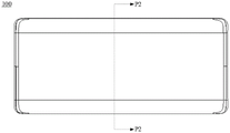
Fig. 9 is a third schematic structural diagram of an electronic device according to an embodiment of the present application.
FIG. 10 is a schematic sectional view taken along line P2-P2 in FIG. 9.
Fig. 11 is an enlarged schematic view of the structure at C in fig. 10.
Detailed Description
The embodiment of the application provides electronic equipment. The electronic device may be a smart phone, a tablet computer, or other devices, and may also be a game device, an AR (Augmented Reality) device, an automobile device, a data storage device, an audio playing device, a video playing device, a notebook computer, a desktop computing device, or other devices.
Referring to fig. 1 and fig. 2, fig. 1 is a first schematic structural diagram of an electronic device according to an embodiment of the present disclosure, and fig. 2 is an exploded schematic structural diagram of the electronic device in fig. 1; the electronic device 100 may include a display screen 10, a shutter, a middle frame 20, a cover plate 30, and a rear cover 40.
The display screen 10 may be used to display information such as images, text, etc. The Display screen 10 may be a Liquid Crystal Display (LCD) or an Organic Light-Emitting Diode (OLED) Display screen.
The display screen 10 may be mounted on the middle frame 20 and connected to the rear cover 40 through the middle frame 20 to form a display surface of the electronic device 100. The display screen 10 and the cover 30 may together serve as a front housing of the electronic device 100, and together with the rear cover 40, form a housing of the electronic device 100 for accommodating other electronic components or functional components of the electronic device 100. For example, the housing may be used to house electronic devices or functional components of the electronic device 100 such as a processor, memory, one or more sensors, a camera module, and the like. It is understood that the cover 30 may not be provided on the display screen 10.
The display screen 10 may include a display area. The display area is used for performing a display function of the display screen 10, for example, displaying information such as images and texts. At this time, functional components such as a camera module and a proximity sensor in the electronic device 100 can be hidden under the display screen 10, and a fingerprint identification module of the electronic device 100 can be disposed on the rear cover 40 of the electronic device 100, so that a full-screen display of the display screen 10 can be realized, and the electronic device 100 can have a large screen occupation ratio.
The display screen 10 may be a flexible screen made of a flexible material, so that the display screen 10 is foldable and bendable, and the display screen 10 made of the flexible material is conveniently mounted on the cover plate 30 with a radian.
Referring to fig. 3, fig. 3 is a schematic structural diagram of a display screen of an electronic device according to an embodiment of the present application. The display screen 10 further includes a main body 11 and a side body 12 connected to each other. The main body 11 may have a planar structure, and when the main body 11 is mounted on the middle frame 20, the planar structure of the main body 11 may be attached to a surface of the middle frame 20 to be stably mounted on the middle frame 20.
The main body 11 may have a rigid planar structure so that the electronic device 100 has a fixed form; the main body 11 may also be a flexible planar structure, and the flexible main body 11 may be deformed under an external force to form a bendable and foldable display structure.
The main body 11 may include a first display surface 111 and a first non-display surface 112 that are oppositely disposed, when viewed from the outside of the electronic device 100 by a user, the first display surface 111 is a surface visible to the main body 11, and the first display surface 111 is used for displaying information; the first non-display surface 112 is a surface invisible to the main body portion 11, the first non-display surface 112 is used for connecting with the middle frame 20, and most of the electronic devices or functional components in the electronic apparatus 100 are disposed on the first non-display surface 112 side of the main body portion 11.
The side body 12 is connected to the main body 11, and the side body 12 is bent toward a side of the main body 11 where a non-display surface is located, such as the first non-display surface 112, wherein the side body 12 may be a planar structure, and the side body 12 may be a rigid planar structure, so that the electronic device 100 has a fixed form; the side body portions 12 may also be flexible planar structures, and the flexible side body portions 12 may be deformed by an external force to form a flexible and foldable display structure.
It is understood that the side body 12 may be a curved structure, and the side body 12 may be a rigid curved structure, so that the electronic device 100 has a fixed form; the side body 12 may also be a flexible curved structure, and the flexible side body 12 may be deformed under an external force to form a bendable and foldable display structure.
It is understood that when the side body 12 has a curved structure, the side body 12 may have a concave curved structure, or the side body 12 may have a convex curved structure, wherein the concave curved structure may be formed by one surface of the side body 12 being concave toward the inside of the electronic device 100, and the convex curved structure may be formed by one surface of the side body 12 being convex toward the outside of the electronic device 100.
It should be noted that the degree of the recess or the degree of the protrusion of the side body 12 may be set according to the actual situation of the electronic device 100, and the embodiment of the present application is not further limited.
The side body 12 may include a second face 121 and a third face 122, which are oppositely disposed, and when viewed from the outside of the electronic device, the second face 121 is a face of the side body 12 that is visible to a user, and the second face 121 is used for displaying information. The third surface 122 is a surface invisible to the side body 12, and the third surface 122 is used for connecting with other parts of the electronic apparatus to fix the side body 12. The third surface 122 of the side body 12 may be directly in contact with and connected to the side wall of the middle frame 20, or the third surface 122 of the side body 12 may be indirectly connected to the side wall of the middle frame via another connecting member.
It should be noted that in the description of the present application, terms such as "first", "second", and the like are used only for distinguishing similar objects, and are not to be construed as indicating or implying relative importance or implicitly indicating the number of technical features indicated.
It should be noted that the physical keys on the electronic device according to the embodiment of the present application may be disposed on the side surfaces of other electronic devices without the side body portion 12; the exposed physical keys of the electronic equipment can be cancelled and replaced by the pressure touch keys under the screen; alternatively, related software programs may be designed to replace the physical keys.
The side body 12 may be bent toward the first non-display surface 111 of the main body 11 on the side of the main body 11. For example, the side body 12 may be bent toward the first non-display surface 111 of the main body 11 at the top side of the main body 11 to form a top side body; forming a bottom side body portion on the bottom side of the main body portion 11 toward the first non-display surface 111 of the main body portion 11; a left body portion formed on the left side of the main body portion 11 toward the first non-display surface 111 of the main body portion 11; the right side body portion is formed on the right side of the body portion 11 toward the first non-display surface 111 of the body portion 11.
The plurality of side body portions 12 may face the first non-display surface 111 of the main body portion 11 on a plurality of sides of the main body portion 11. For example, the opposite side body portions 12 are formed on the first non-display surface 111 of the main body portion 11 on opposite sides of the main body portion 11. For example, two adjacent side body portions 12 are formed on the first non-display surface 111 of the main body portion 11 on both adjacent sides of the main body portion 11. Alternatively, a plurality of side body portions 12 are formed by bending all the side portions of the main body portion 11 toward the first non-display surface 111 of the main body portion 11.
When the main body 11 displays information, the side body 12 can display additional information related thereto. For example, information such as video, pictures, text, etc. may be displayed on the main body part 11, and information such as channels, volume, subtitles, function buttons, etc. may be displayed on the side body part 12. Of course, the side body 12 may display the additional information alone regardless of the information displayed on the main body 11, and for example, the side body 12 may be used to display time or the like when the main body 11 is in the closed state. That is, the main body 11 and the side body 12 of the embodiment of the present application may operate together, and the main body 11 and the side body 12 may operate independently of each other.
The display screen 10 may include a non-display area 123, the non-display area 123 may be provided in the side body portion 12, and the non-display area 123 may not be used for displaying information. The non-display area 123 may be an edge area of the side body part 12, that is, the non-display area 123 may be an area of the side body part 12 away from the main body part 11. Among them, the edge regions of the side body 12 are the edge regions of the side second surface 121 and the third surface 122.
The non-display area 123 of the side body portion 12 may be a Black Matrix (BM), referred to as a BM region for short. The BM regions are provided to prevent light leakage from the display panel 10 during display, and if there are no BM regions, significant halos are seen at the edges of the panel. Therefore, the BM regions, i.e. the black frames, generally exist at the edges of the display screen 10, but the display effect of the display screen 10 is affected by the arrangement of the black frames at the periphery of the display screen 10, so that the present application provides the shielding member at the side of the display surface of the side body portion 12, and the shielding member is connected to the non-display region of the side body portion 12. Therefore, the shielding part can shield the non-display area 123, the black frame at the edge of the display screen 10 can be hidden, the appearance color types of the electronic equipment are reduced, and the appearance effect of the electronic product is improved.
The shielding member is mainly used for shielding the non-display area 123 of the side body portion 12, and may be a part of the middle frame, or may be a separate member, for example, a decorative strip, a decoration, or the like. The color of the shielding piece can be consistent with that of the middle frame, so that the appearance color types of the electronic equipment are reduced, and the appearance effect of the electronic product can be improved.
Referring to fig. 4, fig. 5 and fig. 6, fig. 4 is a schematic structural diagram of a middle frame of an electronic device according to an embodiment of the present disclosure, fig. 5 is a schematic structural diagram of a cross section taken along a direction P1-P1 in fig. 4, and fig. 6 is an enlarged structural diagram of a portion a in fig. 5. The middle frame 20 may have a thin plate-like or sheet-like structure, or may have a hollow frame structure. The middle frame 20 is used for providing a supporting function for the electronic devices or functional components in the electronic device 100, so as to mount the electronic devices or functional components in the electronic device 100 together. For example, functional components such as a camera module, a receiver module, a circuit board, and a battery in the electronic apparatus 100 may be mounted on the middle frame 20 for fixing. Moreover, the material of the middle frame 20 may include metal or plastic.
The middle frame 20 is partially located on the non-display side of the display screen 10, that is, the middle frame 20 may be partially located in a space formed by the first non-display surface 112 of the main body portion 11 and the third surface 122 of the side body portion 12.
The middle frame 20 may include a substrate 21 and a frame portion disposed around the substrate 21, that is, the frame portion is disposed around the substrate 21.
The substrate 21 may include a first side surface 211 and a first surface 213 and a second surface 213 disposed opposite to each other, wherein the first side surface 211 is disposed between the first surface 212 and the second surface 213 and surrounds the first surface 212 and the second surface 213, the first surface 212 is disposed toward the non-display surface of the display screen 10, the second surface 213 is disposed toward the rear cover 40, the non-display surface of the display screen 10 is connected to the first surface 212 of the substrate 21, and the rear cover 40 is connected to the second surface 213 of the substrate 21.
The first surface 212 and the second surface 213 of the substrate 21 may be planar structures, and the first surface 212 and the second surface 213 of the substrate 21 may also be curved structures, or the first surface 212 of the substrate 21 may be a curved structure and the second surface 213 may be a planar structure, which is not further limited in this embodiment of the application.
The first surface 212 may be connected to the first non-display surface 111 of the main body 11, so that the middle frame 20 provides a supporting force for the main body 11.
The first surface 212 may be a planar structure, and the planar structure of the first surface 212 may be closely attached to the first non-display surface 111 of the main body 11, so that the main body 11 is more closely connected to the middle frame 20, and the middle frame 20 may uniformly bear the weight of the main body 11.
The second surface 213 may be directly or indirectly connected to an inner surface of a rear cover 40 of the electronic device 100, and the rear cover 40 covers an outer side of the middle frame 20 to protect electronic devices and the like provided on the middle frame 20.
As shown in fig. 5 and 6, when the shielding member 22 is a part of the middle frame 20, the shielding member 22 corresponds to a frame portion of the substrate 21 corresponding to the non-display area 123 of the side body portion 12, and the shielding member 22 is connected to the outer periphery of the substrate 21, for example, the shielding member 22 can be connected to the first side surface 211 of the substrate 21 and connected to the non-display area 123 through the shielding member 22, so that the shielding member 22 shields the non-display area 123 of the side body portion 12, and thus the shielding member 22 can shield the black frame of the display screen 10, reduce the appearance color of the electronic device 100, and further improve the appearance effect of the electronic device 100. The shield 22 and the substrate 21 are integrated.
It can be understood that the middle frame 20 may further include a connecting portion 23, the shielding member 22 is connected to the substrate 21 through the connecting portion 23, a predetermined angle is formed between the shielding member 22 and the connecting portion 23, the shielding member 22 and the substrate 21 form an accommodating space, and the non-display area 123 of the side body portion 12 is disposed in the accommodating space, so that the shielding member 22 is better connected to the non-display area 123. The shield 22 is integrated with the substrate 21 and the connecting portion 23.
It should be noted that, the above-mentioned angle of predetermineeing can be right angle, obtuse angle and acute angle, and the angle of predetermineeing specifically can set up according to the side somatic part of display screen and the crooked degree of main part, and this application embodiment is no longer repeated one by one.
It is understood that the middle frame 20 may not be provided with the connecting portion 23, and the shielding member 22 may be directly connected to the first side surface 211 of the substrate 21, wherein the shielding member 22 includes a second side surface and a third surface and a fourth surface which are oppositely arranged, the second side surface is arranged between the third surface and the fourth surface and is arranged around the third surface and the fourth surface, the third surface is arranged towards the side where the non-display surface of the main body portion 11 of the display screen 10 is located, and the fourth surface is arranged towards one surface of the rear cover 40. The second side surface of the shielding member 22 is connected to the first side surface 211 of the substrate 21, and the third surface of the shielding member 22 is protruded from the first surface 212 of the substrate 21, so that the portion of the shielding member 22 protruded from the first surface 212 of the substrate 21 is connected to the non-display area 123 of the side body portion 12, that is, the portion of the shielding member 22 protruded from the first surface 212 of the substrate 21 is connected to the non-display area 123 of the side body portion 12 toward the side body portion 12.
It is understood that when the electronic device 100 is not provided with a cover plate, the shutter 22 may be directly connected to the non-display area 123 of the side body portion 12. When the shielding member 22 is a part of the middle frame, that is, when the shielding member 22 is integrally molded with the substrate 21 and the connecting portion 23, the electronic device may further include an adhesive member, and the shielding member 22 is adhered to the non-display area 123 of the side body portion 12 by the adhesive member, so that the shielding member 22 is connected to the non-display area 123.
The adhesive member may be a foam double-sided tape, one surface of the foam double-sided tape is connected to the non-display area 123 of the side body portion 12, and the other surface of the foam double-sided tape is connected to one surface of the shielding member 22 facing the side body portion 12, so that the shielding member 22 and the non-display area 123 of the side body portion 12 are adhered together by the foam double-sided tape.
The shielding member 22 and the non-display area 123 of the side body portion 12 are connected together by a foam double-sided adhesive tape, on one hand, the foam double-sided adhesive tape has good compression performance, and the foam double-sided adhesive tape occupies less space; on the other hand, the foam double-sided adhesive has good impact absorption, and connects the shielding member 22 and the non-display area 123 of the side body 12 together, so that the edge warping probability when the two are bonded can be reduced, and the two are connected more firmly.
It will be understood that the cover 22 can also be inserted into the non-display area 123 of the side body 12, so that the cover 22 can be inserted into the non-display area 123 of the side body 12.
For example, a first protrusion is disposed on a surface of the shielding member 22 facing the non-display area 123 of the side body 12, and a first groove is disposed on the non-display area 123 of the side body 12, wherein the first groove is disposed on a side where the display surface of the side body 12 is located, and the first protrusion is embedded in the first groove to connect the shielding member 22 and the side body 12.
For another example, a second groove is formed on a surface of the shielding member 22 facing the non-display area 123 of the side body portion 12, and a second protrusion is formed on the non-display area 123 of the side body portion 12, wherein the second protrusion is disposed on a side where the display surface of the side body portion 12 is located, and the second protrusion is embedded in the second groove to connect the shielding member 22 and the side body portion 12.
It can be understood that, in the electronic device 100 of the embodiment of the present application, the shielding member 22 and the non-display area 123 of the side body 12 can also be adhered and clamped together at the same time, so that the shielding member 22 and the non-display area 123 of the side body 12 are combined more tightly.
It will be appreciated that in order to make the fitting of the shutter 22 with the non-display area 123 of the side body portion 12 smoother, the non-display area 123 of the side body portion 12 is provided with an installation space for accommodating the shutter 22.
The installation space is matched with the shielding member 22, that is, the shape and size of the installation space are matched with the shielding member 22, so that the shielding member 22 is connected with the non-display area 123 of the side body portion 12 smoothly without a protrusion, and the appearance of the electronic device 100 can be more beautiful.
It is understood that, in order not to affect other electronic components disposed in the non-display area, the installation space may be an opening cut out in the non-display area by a cutter, and the thickness of the opening is very small, and the thickness of the shutter 22 is also very small and is consistent with the thickness of the opening.
When the shielding member 22 is a separate member, that is, the shielding member 22 is not integrally provided with the substrate 21 and the connecting portion 23, and a frame portion may not be provided on the side edge of the substrate 21 corresponding to the non-display area 123, in this case, the shielding member 22 may be connected to the connecting portion 23 instead of the frame portion, and the shielding member 22 may be connected to the first surface of the connecting portion 23, so that one surface of the shielding member 22 facing the side body portion 12 is connected to the non-display area 123; the first surface is a surface of the connecting portion 23 facing the main body portion 11.
The shielding element 22 and the first surface of the connecting portion 23 have a predetermined angle therebetween, which may be a right angle, an acute angle, or the like, and the angle between the shielding element and the first surface of the connecting portion 23 may be matched with the bending curvature of the side body portion 12, so that the shielding element 22 is better attached to and connected to the non-display area 123 of the side body portion 12.
For example, the shielding member 22 may be a decorative strip, the decorative strip may be directly connected to the non-display area 123 of the side body 12 by means of bonding, clipping, or the like, and the shielding member 22 may be connected to the middle frame 20 by means of bonding, clipping, or the like, and connected to the non-display area 123 of the side body 12 through the middle frame 20.
Wherein, the first face of connecting portion 23 is equipped with first joint portion, shielding piece 22 is equipped with second joint portion, first joint portion with second joint portion mutually supports, in order to realize shielding piece 22 with connecting portion 23's connection.
The limiting groove can be formed in the first clamping portion, the second clamping portion can be limiting blocks and clamped in the limiting grooves through the limiting blocks, so that the first clamping portion is connected with the second clamping portion, and the shielding piece 22 can be connected to the connecting portion 23 of the middle frame 20.
First joint portion can be the stopper, can seted up the spacing groove in the second joint portion, through stopper joint in the spacing groove to make first joint portion be connected with second joint portion, thereby can realize that shielding member 22 connects in the connecting portion 23 of center 20.
The electronic device further comprises a first adhesive piece, and the shielding piece 22 is adhered to the first surface of the connecting part 23 through the first adhesive piece, so that the shielding piece 22 is connected to the connecting part 23.
Wherein, first bonding piece can be the cotton double faced adhesive tape of bubble, and the one side of the cotton double faced adhesive tape of bubble is connected with the first face of connecting portion 23, and the another side and the shielding piece 22 of the cotton double faced adhesive tape of bubble are connected, and then through the cotton double faced adhesive tape of bubble, connecting portion 23 and shielding piece 22 are bonded together.
The first surface of the connecting part 23 and the shielding part 22 are connected together through the foam double-sided adhesive tape, so that on one hand, the foam double-sided adhesive tape has good compression performance, and the space occupied by the foam double-sided adhesive tape is small; on the other hand, the foam double-sided adhesive tape has good impact absorbability, and the foam double-sided adhesive tape connects the connecting part 23 and the shielding part 22 together, so that the edge warping probability when the foam double-sided adhesive tape is bonded can be reduced, and the foam double-sided adhesive tape and the shielding part are connected more firmly.
It will be appreciated that the shield 22 may not be connected to the center frame 20, and the shield 22 may be directly connected to the non-display area 123 of the side body 12. For example, a male snap member can be disposed on the non-display area 123 of the side body portion 12, correspondingly, a female snap member is disposed on one surface of the shielding member 22 facing the side body portion 12, the male snap member is embedded in the female snap member, and the shielding member 22 is clamped with the non-display area 123 of the side body portion 12, so that the shielding member 22 can shield the non-display area 123, the purpose of hiding the black frame of the side body portion 12 is achieved, and the display effect of the display screen 10 can be improved.
A female snap member may be disposed on the non-display area 123 of the side body 12, and correspondingly, a male snap member may be disposed on a side of the shielding member facing the side body 12, the male snap member is engaged with the female snap member, and the shielding member is engaged with the non-display area 123 of the side body 12.
For another example, in the electronic device according to the embodiment of the present application, glue may be filled between the non-display area 123 of the side body 12 and the shielding member 22 by using a dispenser, and after the glue is solidified, the shielding member and the non-display area 123 of the side body 12 are bonded together. The glue can be shadowless glue, silica gel and the like.
For another example, the electronic device according to the embodiment of the present application further includes a second adhesive, and the shielding member 22 is adhered to the non-display area 123 of the side body portion 12 by the second adhesive, so as to connect the shielding member 22 and the non-display area 123.
The second adhesive member may be a foam double-sided tape, one surface of the foam double-sided tape is connected to the non-display area 123 of the side body 12, and the other surface of the foam double-sided tape is connected to one surface of the shielding member 22 facing the non-display area 123, so that the shielding member and the non-display area 123 of the side body 12 are adhered together by the foam double-sided tape.
The shielding member 22 and the non-display area 123 of the side body portion 12 are connected together by a foam double-sided adhesive tape, on one hand, the foam double-sided adhesive tape has good compression performance, and the foam double-sided adhesive tape occupies less space; on the other hand, the foam double-sided adhesive has good impact absorption, and connects the shielding piece and the non-display area 123 of the side body part 12 together, so that the edge warping probability when the shielding piece and the side body part are bonded can be reduced, and the connection between the shielding piece and the side body part is firmer.
It can be understood that, in the electronic device of the embodiment of the present application, the shielding member 22 and the non-display area 123 of the side body 12 can also be adhered and clamped together at the same time, so that the shielding member 22 and the non-display area 123 of the side body 12 are combined more tightly.
Referring to fig. 7 and 8, fig. 7 is a second structural schematic diagram of an electronic device according to an embodiment of the present application, and fig. 8 is an enlarged structural schematic diagram of a portion B in fig. 7; the electronic device 100 further includes a cover 30, and the cover 30 covers the main body 11 and the side body 12 of the display 10 to protect the main body 11 and the side body 12 and prevent the main body 11 and the side body 12 from being scratched or damaged by water. The cover plate 30 may be a transparent glass cover plate, so that a user can see through the cover plate 30 to observe contents displayed on the main body 11 and the side body 12, and the cover plate 30 may be a glass cover plate made of sapphire.
The cover 30 may include a first portion 31 and a second portion 32, the second portion 32 is connected to the first portion 31, the first portion 31 is connected to the first display surface of the main body 11, and the second portion 32 is connected to the third surface of the side body 12.
The first portion 31 may have a planar structure, and the shape and size of the first portion 31 are matched with the shape and size of the main body 11, so that the main first portion 31 can better cover the main body 11 of the display screen 10, on one hand, the main body 11 of the display screen 10 is better protected, and on the other hand, the appearance of the electronic device 100 can be more beautiful.
The second portion 32 is bent toward the side of the main body 11 where the first display surface 111 is located, and the second portion 32 may have a planar structure or a curved structure. The bending angle and the size of the second portion 32 are matched with those of the side body 12 of the display screen 10, so as to better cover the side body 12 of the display screen 10.
The second portion 32 may include a first connection face 321 and a second connection face 322, which are oppositely disposed, the first connection face 321 is a face of the second portion 32 that is visible when a user views from the outside of the electronic device, and the second connection face 322 is a face that is not visible by the second portion 32, that is, the second connection face 322 is a face that is connected to the third face 122 of the side body 12 of the display screen 10, and the second connection face 322 is used for being connected to the third face 122 of the display screen 10 of the electronic device to fix the second portion 32.
The second portion 32 may further include a connection region 323, the connection region 323 is disposed opposite to the non-display region 123 of the side body portion 12, and the shielding member is connected to the connection region 323, so that the shielding member shields the non-display region 123, thereby shielding a black frame of the display screen 10 by the shielding member, reducing the appearance color category of the electronic device 100, and further improving the appearance effect of the electronic device 100.
The shape and size of the connection area 323 of the second portion 32 are both matched with the non-display area 123 of the side body 12, the shielding member is connected to the connection area 323, and is connected to the connection area 323 through the shielding member, so that the shielding member can shield the non-display area 123 of the side body 12, thereby hiding the black frame of the display screen 10, reducing the appearance color types of the electronic device 100, and further improving the appearance effect of the electronic device 100. When the shielding element is a part of the middle frame 20, that is, the shielding element and the middle frame 20 are an integral structure, the shielding element 22 is connected to the connection region 323, so that the shielding element 22 shields the non-display region 123 of the side body portion 12, thereby hiding the black frame of the display screen 10, reducing the appearance color types of the electronic device 100, and further improving the appearance effect of the electronic device 100.
It should be noted that, in the embodiment of the present application, reference may be made to the connection manner between the shielding member 22 and the connection region, and details are not repeated herein.
When the shielding member 22 is a separate component, the shielding member 22 can be connected to the first surface of the connecting portion 23 of the middle frame 20, so that the shielding member 22 is connected to the connecting area 323 of the second portion 32, wherein the connection manner between the shielding member 22 and the connecting portion 23 is as described above, and is not described in detail herein.
Referring to fig. 9, fig. 10 and fig. 11 in combination with fig. 8, fig. 9 is a third structural schematic diagram of an electronic device according to an embodiment of the present application, fig. 10 is a schematic cross-sectional structure diagram at P2-P2 in fig. 9, and fig. 11 is an enlarged structural schematic diagram at C in fig. 10. It can be understood that, in order to make the connection between the shielding element 22 and the connection region 323 of the second portion 32 smooth and without protrusion, the connection region 323 of the second portion 32 of the embodiment of the present application is further provided with an avoiding space 3231, the avoiding space 3231 is used for accommodating the shielding element 22, the shielding element 22 is adapted to the avoiding space 3231, and by connecting the shielding element 22 to the avoiding space 3231, the connection between the shielding element 22 and the side body portion 32 is smooth and without protrusion, so that the appearance of the electronic device 100 can be more beautiful.
The avoiding space 3231 may be an opening formed by cutting off the connecting area 323 of the second portion 32, and the shape and size of the opening are matched with those of the shielding member 22, so as to better connect the shielding member 22 and the connecting area 323 of the second portion 32.
It can be understood that, in the embodiment of the present application, the thickness of the second portion 32 of the cover plate 30 is greater than that of the first portion 31, so that the structural strength of the second portion 32 can be prevented from being affected by the provision of the escape space 3231 in the second portion 32 of the cover plate 30.
Specifically, the thickness of the second portion 32 at the position corresponding to the connection region 323 is greater than the thickness of the first portion 31, that is, the thickness of the connection region 323 is greater than the thickness of the first portion 31; alternatively, the thickness of the connection region 323 is greater than the thickness of the regions of the first and second portions 31 and 32 other than the connection region 323.
The electronic device 100 further includes a third adhesive member, and the shielding member 22 is adhered to the avoiding space 3231 of the connection region 323 by the third adhesive member, so as to connect the shielding member 22 and the avoiding space 3231 of the connection region 323.
The third bonding member may be a foam double-sided adhesive tape, one surface of the foam double-sided adhesive tape is bonded to the avoiding space 3231 of the connection region 323, the other surface of the foam double-sided adhesive tape is connected to one surface of the shielding member facing the connection region 323, and the shielding member 22 and the avoiding space 3231 of the connection region 323 are bonded together through the foam double-sided adhesive tape.
The shielding piece 22 and the avoiding space 3231 of the connecting area 323 are connected together through the foam double-sided adhesive tape, so that on one hand, the foam double-sided adhesive tape has good compression performance, and the foam double-sided adhesive tape occupies less space; on the other hand, the foam double-sided adhesive has good impact absorption, and connects the shielding piece and the non-display area 123 of the side body part 12 together, so that the edge warping probability when the shielding piece and the side body part are bonded can be reduced, and the connection between the shielding piece and the side body part is firmer.
It is understood that, in the electronic device according to the embodiment of the present application, the shielding member 22 and the connecting region 323 can also be adhered and snapped together at the same time, so that the shielding member 22 and the avoiding space 3211 of the connecting region 323 can be combined more tightly.
The rear cover 40 is used to form an outer contour of the electronic device 100. The rear cover 40 may be integrally formed. In the forming process of the rear cover 40, structures such as a rear camera module hole, a fingerprint identification module mounting hole and the like can be formed on the rear cover 40.
The rear cover 40 may be made of metal, such as magnesium alloy, stainless steel, etc. Note that the material of the rear cover 40 according to the embodiment of the present application is not limited to this, and other methods may be adopted. For example, the rear cover 40 may be made of plastic. For another example, the rear cover 40 may be made of ceramic or glass. For another example, the rear cover 40 may include a plastic material and a metal material, and the rear cover 40 may be a housing structure in which the metal and the plastic are matched with each other. Specifically, the metal part may be formed first, for example, a magnesium alloy substrate is formed by injection molding, and then plastic is injected on the magnesium alloy substrate to form a plastic substrate, so as to form a complete housing structure.
In addition, the electronic device 100 of the embodiment of the present application may further include a circuit board, a battery, and the like. Among them, the circuit board may be mounted on the middle frame 20, and particularly, the circuit board may be mounted in a space between the substrate of the middle frame 20 and the rear cover 40. The circuit board may be a motherboard of the electronic device 100. One, two or more of functional components such as a microphone, a loudspeaker, a receiver, an earphone interface, a universal serial bus interface (USB interface), a camera component, a distance sensor, an ambient light sensor, a gyroscope, a processor and the like can be integrated on the circuit board. Meanwhile, the display screen 10 may be electrically connected to a circuit board.
The circuit board may be provided with a display control circuit. The display control circuit outputs an electric signal to the display screen 10 to control the main body portion 11 and the side body portion 12 of the display screen 10 to display information.
The battery may be mounted on the middle frame 20. Meanwhile, the battery is electrically connected to the circuit board to enable the battery to power the electronic device 100. Wherein, the circuit board can be provided with a power management circuit. The power management circuit is used to distribute the voltage provided by the battery to the various electronic devices in the electronic apparatus 100.
The battery may be a rechargeable battery. For example, the battery may be a lithium ion battery.
It is understood that the electronic device 100 of the embodiment of the present application may further include other functional components and electronic devices, for example, a microphone, a speaker, a receiver, a camera module, a proximity sensor, a fingerprint identification module, and the like. The structures and mounting positions of these electronic devices and functional components can be referred to in the related art, and are not described in detail in the embodiments of the present application.
The electronic device provided by the embodiment of the present application is described in detail above. The principle and the implementation of the present application are explained herein by applying specific examples, and the above description of the embodiments is only used to help understand the method and the core idea of the present application; meanwhile, for those skilled in the art, according to the idea of the present application, there may be variations in the specific embodiments and the application scope, and in summary, the content of the present specification should not be construed as a limitation to the present application.
Claims (11)
1. An electronic device, comprising:
the display screen comprises a main body part and a side body part, wherein the side body part is connected with the main body part, is bent towards one side of the main body part where a non-display surface is located, and comprises a non-display area; and
and the shielding piece is arranged on one side of the display surface of the side body part and is connected to the non-display area so as to shield the non-display area.
2. The electronic device of claim 1, further comprising:
the middle frame comprises a base plate, the shielding piece is connected to the outer peripheral edge of the base plate, and the base plate and the shielding piece are of an integral structure.
3. The electronic device of claim 2, wherein the middle frame further comprises:
the connecting portion, the shielding piece pass through the connecting portion with the base plate is connected, just the shielding piece with be formed with preset angle between the connecting portion, shielding piece with the base plate forms an accommodation space, the non-display area of side somatic part set up in the accommodation space.
4. The electronic device of claim 1, further comprising:
the middle frame comprises a base plate and a connecting part, the connecting part is connected to the outer periphery of the base plate, and the shielding piece is connected to the first surface of the connecting part;
wherein the first surface is a surface of the connecting portion facing the main body portion.
5. The electronic device according to claim 4, wherein a first clamping portion is disposed on the first surface of the connecting portion, and a second clamping portion is disposed on the shielding member, and the first clamping portion and the second clamping portion are matched with each other to connect the shielding member to the connecting portion.
6. The electronic device of claim 4, further comprising:
the shielding piece is adhered to the first surface of the connecting part through the first adhesive piece, so that the shielding piece is connected to the connecting part.
7. The electronic device according to claim 1, wherein the non-display region of the side body portion is provided with an installation space, the installation space is provided corresponding to the non-display region, the shielding member is provided in the installation space, and the shielding member is adapted to the installation space.
8. The electronic device of claim 1, further comprising:
the cover plate is arranged on the display screen and comprises a first part and a second part, the second part is connected to the first part, the first part is connected to the display surface of the main body part, the second part is connected to the display surface of the side body part, the second part comprises a connecting area, the non-display area and the connecting area are correspondingly arranged, and the shielding piece is connected to the connecting area.
9. The electronic device according to claim 8, wherein the connection area is provided with an avoidance space, the shielding member is located in the avoidance space, and the shielding member is adapted to the avoidance space.
10. The electronic device of claim 8, further comprising:
the shielding piece is adhered to the connecting area through the second adhesive piece, so that the shielding piece is connected with the connecting area.
11. The electronic device of any of claims 8-10, wherein a thickness of the second portion is greater than a thickness of the first portion.
Priority Applications (1)
| Application Number | Priority Date | Filing Date | Title |
|---|---|---|---|
| CN201921691158.2U CN210380944U (en) | 2019-10-09 | 2019-10-09 | Electronic device |
Applications Claiming Priority (1)
| Application Number | Priority Date | Filing Date | Title |
|---|---|---|---|
| CN201921691158.2U CN210380944U (en) | 2019-10-09 | 2019-10-09 | Electronic device |
Publications (1)
| Publication Number | Publication Date |
|---|---|
| CN210380944U true CN210380944U (en) | 2020-04-21 |
Family
ID=70256155
Family Applications (1)
| Application Number | Title | Priority Date | Filing Date |
|---|---|---|---|
| CN201921691158.2U Active CN210380944U (en) | 2019-10-09 | 2019-10-09 | Electronic device |
Country Status (1)
| Country | Link |
|---|---|
| CN (1) | CN210380944U (en) |
Cited By (1)
| Publication number | Priority date | Publication date | Assignee | Title |
|---|---|---|---|---|
| CN112261183A (en) * | 2020-10-20 | 2021-01-22 | 北京字节跳动网络技术有限公司 | Display screen module and terminal |
-
2019
- 2019-10-09 CN CN201921691158.2U patent/CN210380944U/en active Active
Cited By (2)
| Publication number | Priority date | Publication date | Assignee | Title |
|---|---|---|---|---|
| CN112261183A (en) * | 2020-10-20 | 2021-01-22 | 北京字节跳动网络技术有限公司 | Display screen module and terminal |
| CN112261183B (en) * | 2020-10-20 | 2022-07-12 | 北京字节跳动网络技术有限公司 | Display screen module and terminal |
Similar Documents
| Publication | Publication Date | Title |
|---|---|---|
| CN108254975B (en) | Display screen assembly and electronic equipment | |
| US10171896B2 (en) | Electronic device with side speaker hole | |
| US9891734B2 (en) | Mobile terminal display structure and mobile terminal | |
| US20180199457A1 (en) | Display assembly, electronic device and method for assembling the same | |
| EP3176671B1 (en) | Display screen assembly and terminal | |
| EP4184903A1 (en) | Electronic device including acoustic module | |
| EP2517540B1 (en) | A housing for a portable electronic device | |
| CN110572492A (en) | Electronic device | |
| CN108881539B (en) | Display screen assembly and electronic equipment | |
| AU2013251253B2 (en) | Electronic device | |
| CN210137348U (en) | Electronic equipment | |
| CN108132563B (en) | Backlight module, display screen and electronic equipment | |
| CN109413246B (en) | Shell assembly and electronic equipment | |
| US9380716B2 (en) | Mobile terminal and method of fabricating case thereof | |
| CN108234702B (en) | Display screen assembly and electronic equipment | |
| CN211928482U (en) | Electronic device | |
| EP3598722A1 (en) | Mobile terminal | |
| JP2020504841A (en) | Display device assembly, electronic device, and method for assembling them | |
| CN113037894B (en) | Electronic equipment | |
| CN210137422U (en) | Electronic equipment | |
| CN111010466B (en) | Electronic device and display screen installation method | |
| CN210380944U (en) | Electronic device | |
| US20200028948A1 (en) | Mobile terminal | |
| CN108540616B (en) | Display screen assembly and electronic equipment | |
| CN211928483U (en) | Electronic device |
Legal Events
| Date | Code | Title | Description |
|---|---|---|---|
| GR01 | Patent grant | ||
| GR01 | Patent grant |