CN1877448A - Etchant, method for fabricating a wire using the etchant, and method for fabricating a thin film transistor substrate using the etchant - Google Patents
Etchant, method for fabricating a wire using the etchant, and method for fabricating a thin film transistor substrate using the etchant Download PDFInfo
- Publication number
- CN1877448A CN1877448A CNA2006100674071A CN200610067407A CN1877448A CN 1877448 A CN1877448 A CN 1877448A CN A2006100674071 A CNA2006100674071 A CN A2006100674071A CN 200610067407 A CN200610067407 A CN 200610067407A CN 1877448 A CN1877448 A CN 1877448A
- Authority
- CN
- China
- Prior art keywords
- layer
- etchant
- conductive oxide
- scope
- oxide layer
- Prior art date
- Legal status (The legal status is an assumption and is not a legal conclusion. Google has not performed a legal analysis and makes no representation as to the accuracy of the status listed.)
- Pending
Links
- 238000000034 method Methods 0.000 title claims abstract description 72
- 239000010409 thin film Substances 0.000 title claims abstract description 12
- 239000000758 substrate Substances 0.000 title claims description 62
- 238000005530 etching Methods 0.000 claims abstract description 63
- 239000000463 material Substances 0.000 claims abstract description 38
- USFZMSVCRYTOJT-UHFFFAOYSA-N Ammonium acetate Chemical compound N.CC(O)=O USFZMSVCRYTOJT-UHFFFAOYSA-N 0.000 claims abstract description 17
- XLYOFNOQVPJJNP-UHFFFAOYSA-N water Chemical compound O XLYOFNOQVPJJNP-UHFFFAOYSA-N 0.000 claims abstract description 13
- 239000008367 deionised water Substances 0.000 claims abstract description 11
- 229910021641 deionized water Inorganic materials 0.000 claims abstract description 11
- 229910052760 oxygen Inorganic materials 0.000 claims abstract description 8
- 229910052710 silicon Inorganic materials 0.000 claims abstract description 8
- 125000000217 alkyl group Chemical group 0.000 claims abstract description 7
- 229910052782 aluminium Inorganic materials 0.000 claims abstract description 7
- 229910052788 barium Inorganic materials 0.000 claims abstract description 7
- 229910052796 boron Inorganic materials 0.000 claims abstract description 7
- 229910052804 chromium Inorganic materials 0.000 claims abstract description 7
- 229910052742 iron Inorganic materials 0.000 claims abstract description 7
- 229910052718 tin Inorganic materials 0.000 claims abstract description 7
- 229910052719 titanium Inorganic materials 0.000 claims abstract description 7
- 229910052725 zinc Inorganic materials 0.000 claims abstract description 7
- 239000004065 semiconductor Substances 0.000 claims description 33
- NBIIXXVUZAFLBC-UHFFFAOYSA-N Phosphoric acid Chemical compound OP(O)(O)=O NBIIXXVUZAFLBC-UHFFFAOYSA-N 0.000 claims description 26
- 239000012212 insulator Substances 0.000 claims description 24
- 238000004519 manufacturing process Methods 0.000 claims description 20
- 238000010276 construction Methods 0.000 claims description 17
- 229910001316 Ag alloy Inorganic materials 0.000 claims description 16
- 239000005695 Ammonium acetate Substances 0.000 claims description 15
- 229940043376 ammonium acetate Drugs 0.000 claims description 15
- 235000019257 ammonium acetate Nutrition 0.000 claims description 15
- 230000015572 biosynthetic process Effects 0.000 claims description 15
- 229910052709 silver Inorganic materials 0.000 claims description 15
- 229910000147 aluminium phosphate Inorganic materials 0.000 claims description 13
- QTBSBXVTEAMEQO-UHFFFAOYSA-M Acetate Chemical compound CC([O-])=O QTBSBXVTEAMEQO-UHFFFAOYSA-M 0.000 claims description 10
- GRYLNZFGIOXLOG-UHFFFAOYSA-N Nitric acid Chemical compound O[N+]([O-])=O GRYLNZFGIOXLOG-UHFFFAOYSA-N 0.000 claims description 9
- 229910017604 nitric acid Inorganic materials 0.000 claims description 9
- MRNHPUHPBOKKQT-UHFFFAOYSA-N indium;tin;hydrate Chemical compound O.[In].[Sn] MRNHPUHPBOKKQT-UHFFFAOYSA-N 0.000 claims description 8
- 238000000151 deposition Methods 0.000 claims description 7
- 239000011701 zinc Substances 0.000 claims description 6
- YVTHLONGBIQYBO-UHFFFAOYSA-N zinc indium(3+) oxygen(2-) Chemical compound [O--].[Zn++].[In+3] YVTHLONGBIQYBO-UHFFFAOYSA-N 0.000 claims description 5
- 238000002347 injection Methods 0.000 claims 2
- 239000007924 injection Substances 0.000 claims 2
- 239000003795 chemical substances by application Substances 0.000 abstract description 4
- 239000010410 layer Substances 0.000 description 324
- 229920002120 photoresistant polymer Polymers 0.000 description 60
- 229910021417 amorphous silicon Inorganic materials 0.000 description 38
- 238000002161 passivation Methods 0.000 description 25
- 238000001259 photo etching Methods 0.000 description 17
- 235000019593 adhesiveness Nutrition 0.000 description 15
- 230000008569 process Effects 0.000 description 12
- 230000003647 oxidation Effects 0.000 description 10
- 238000007254 oxidation reaction Methods 0.000 description 10
- 229960004838 phosphoric acid Drugs 0.000 description 10
- 235000011007 phosphoric acid Nutrition 0.000 description 10
- 239000004005 microsphere Substances 0.000 description 9
- 229910052581 Si3N4 Inorganic materials 0.000 description 8
- 239000004973 liquid crystal related substance Substances 0.000 description 8
- HQVNEWCFYHHQES-UHFFFAOYSA-N silicon nitride Chemical compound N12[Si]34N5[Si]62N3[Si]51N64 HQVNEWCFYHHQES-UHFFFAOYSA-N 0.000 description 8
- VYPSYNLAJGMNEJ-UHFFFAOYSA-N Silicium dioxide Chemical compound O=[Si]=O VYPSYNLAJGMNEJ-UHFFFAOYSA-N 0.000 description 7
- 230000008859 change Effects 0.000 description 7
- 239000002184 metal Substances 0.000 description 7
- 229910052751 metal Inorganic materials 0.000 description 7
- 239000011368 organic material Substances 0.000 description 7
- 230000005540 biological transmission Effects 0.000 description 6
- 239000007789 gas Substances 0.000 description 6
- 238000000623 plasma-assisted chemical vapour deposition Methods 0.000 description 5
- 239000000126 substance Substances 0.000 description 5
- 206010034972 Photosensitivity reaction Diseases 0.000 description 4
- 230000001154 acute effect Effects 0.000 description 4
- 239000003990 capacitor Substances 0.000 description 4
- 238000005229 chemical vapour deposition Methods 0.000 description 4
- 230000036211 photosensitivity Effects 0.000 description 4
- IJGRMHOSHXDMSA-UHFFFAOYSA-N Atomic nitrogen Chemical compound N#N IJGRMHOSHXDMSA-UHFFFAOYSA-N 0.000 description 3
- 229910004205 SiNX Inorganic materials 0.000 description 3
- 230000008901 benefit Effects 0.000 description 3
- 230000008021 deposition Effects 0.000 description 3
- 230000000694 effects Effects 0.000 description 3
- 230000005684 electric field Effects 0.000 description 3
- 238000001914 filtration Methods 0.000 description 3
- 229910010272 inorganic material Inorganic materials 0.000 description 3
- 239000011147 inorganic material Substances 0.000 description 3
- 238000009413 insulation Methods 0.000 description 3
- 230000004044 response Effects 0.000 description 3
- 239000000377 silicon dioxide Substances 0.000 description 3
- 239000004094 surface-active agent Substances 0.000 description 3
- 238000002834 transmittance Methods 0.000 description 3
- 238000001039 wet etching Methods 0.000 description 3
- 108010022579 ATP dependent 26S protease Proteins 0.000 description 2
- QGZKDVFQNNGYKY-UHFFFAOYSA-N Ammonia Chemical compound N QGZKDVFQNNGYKY-UHFFFAOYSA-N 0.000 description 2
- GQPLMRYTRLFLPF-UHFFFAOYSA-N Nitrous Oxide Chemical compound [O-][N+]#N GQPLMRYTRLFLPF-UHFFFAOYSA-N 0.000 description 2
- 238000006243 chemical reaction Methods 0.000 description 2
- 238000002425 crystallisation Methods 0.000 description 2
- 230000008025 crystallization Effects 0.000 description 2
- 238000005516 engineering process Methods 0.000 description 2
- 239000011521 glass Substances 0.000 description 2
- 238000005984 hydrogenation reaction Methods 0.000 description 2
- 239000011810 insulating material Substances 0.000 description 2
- 239000011159 matrix material Substances 0.000 description 2
- 150000004767 nitrides Chemical class 0.000 description 2
- 230000000717 retained effect Effects 0.000 description 2
- 235000012239 silicon dioxide Nutrition 0.000 description 2
- 238000004544 sputter deposition Methods 0.000 description 2
- SYSZENVIJHPFNL-UHFFFAOYSA-N (alpha-D-mannosyl)7-beta-D-mannosyl-diacetylchitobiosyl-L-asparagine, isoform B (protein) Chemical compound COC1=CC=C(I)C=C1 SYSZENVIJHPFNL-UHFFFAOYSA-N 0.000 description 1
- 229910004298 SiO 2 Inorganic materials 0.000 description 1
- XUIMIQQOPSSXEZ-UHFFFAOYSA-N Silicon Chemical compound [Si] XUIMIQQOPSSXEZ-UHFFFAOYSA-N 0.000 description 1
- 229940022663 acetate Drugs 0.000 description 1
- YBCVMFKXIKNREZ-UHFFFAOYSA-N acoh acetic acid Chemical compound CC(O)=O.CC(O)=O YBCVMFKXIKNREZ-UHFFFAOYSA-N 0.000 description 1
- 239000000654 additive Substances 0.000 description 1
- 230000000996 additive effect Effects 0.000 description 1
- 239000002671 adjuvant Substances 0.000 description 1
- 229910021529 ammonia Inorganic materials 0.000 description 1
- 239000003945 anionic surfactant Substances 0.000 description 1
- 238000004380 ashing Methods 0.000 description 1
- QVGXLLKOCUKJST-UHFFFAOYSA-N atomic oxygen Chemical compound [O] QVGXLLKOCUKJST-UHFFFAOYSA-N 0.000 description 1
- 239000003093 cationic surfactant Substances 0.000 description 1
- 239000004020 conductor Substances 0.000 description 1
- 230000007423 decrease Effects 0.000 description 1
- 230000000593 degrading effect Effects 0.000 description 1
- 238000005137 deposition process Methods 0.000 description 1
- 230000005611 electricity Effects 0.000 description 1
- 238000006056 electrooxidation reaction Methods 0.000 description 1
- 239000010408 film Substances 0.000 description 1
- 238000010438 heat treatment Methods 0.000 description 1
- 239000001257 hydrogen Substances 0.000 description 1
- 229910052739 hydrogen Inorganic materials 0.000 description 1
- 125000004435 hydrogen atom Chemical class [H]* 0.000 description 1
- 238000001566 impedance spectroscopy Methods 0.000 description 1
- 230000006872 improvement Effects 0.000 description 1
- 239000012535 impurity Substances 0.000 description 1
- 239000012774 insulation material Substances 0.000 description 1
- 238000001459 lithography Methods 0.000 description 1
- 238000012423 maintenance Methods 0.000 description 1
- 229910044991 metal oxide Inorganic materials 0.000 description 1
- 150000004706 metal oxides Chemical class 0.000 description 1
- 238000002156 mixing Methods 0.000 description 1
- 239000000203 mixture Substances 0.000 description 1
- LFLZOWIFJOBEPN-UHFFFAOYSA-N nitrate, nitrate Chemical compound O[N+]([O-])=O.O[N+]([O-])=O LFLZOWIFJOBEPN-UHFFFAOYSA-N 0.000 description 1
- 229940074355 nitric acid Drugs 0.000 description 1
- 229910052757 nitrogen Inorganic materials 0.000 description 1
- QJGQUHMNIGDVPM-UHFFFAOYSA-N nitrogen group Chemical group [N] QJGQUHMNIGDVPM-UHFFFAOYSA-N 0.000 description 1
- 239000001272 nitrous oxide Substances 0.000 description 1
- 229920003986 novolac Polymers 0.000 description 1
- 239000012044 organic layer Substances 0.000 description 1
- 239000001301 oxygen Substances 0.000 description 1
- 229910021420 polycrystalline silicon Inorganic materials 0.000 description 1
- 229920005591 polysilicon Polymers 0.000 description 1
- 238000007639 printing Methods 0.000 description 1
- 238000012797 qualification Methods 0.000 description 1
- 238000010992 reflux Methods 0.000 description 1
- 238000004062 sedimentation Methods 0.000 description 1
- 229910021332 silicide Inorganic materials 0.000 description 1
- FVBUAEGBCNSCDD-UHFFFAOYSA-N silicide(4-) Chemical compound [Si-4] FVBUAEGBCNSCDD-UHFFFAOYSA-N 0.000 description 1
- 239000010703 silicon Substances 0.000 description 1
- 239000002356 single layer Substances 0.000 description 1
- 239000007921 spray Substances 0.000 description 1
- 238000005477 sputtering target Methods 0.000 description 1
- 230000006641 stabilisation Effects 0.000 description 1
- 238000011105 stabilization Methods 0.000 description 1
- 239000003381 stabilizer Substances 0.000 description 1
- 238000005728 strengthening Methods 0.000 description 1
- 229910021642 ultra pure water Inorganic materials 0.000 description 1
- 239000012498 ultrapure water Substances 0.000 description 1
Images


Classifications
-
- H—ELECTRICITY
- H01—ELECTRIC ELEMENTS
- H01L—SEMICONDUCTOR DEVICES NOT COVERED BY CLASS H10
- H01L21/00—Processes or apparatus adapted for the manufacture or treatment of semiconductor or solid state devices or of parts thereof
- H01L21/02—Manufacture or treatment of semiconductor devices or of parts thereof
- H01L21/04—Manufacture or treatment of semiconductor devices or of parts thereof the devices having potential barriers, e.g. a PN junction, depletion layer or carrier concentration layer
- H01L21/18—Manufacture or treatment of semiconductor devices or of parts thereof the devices having potential barriers, e.g. a PN junction, depletion layer or carrier concentration layer the devices having semiconductor bodies comprising elements of Group IV of the Periodic Table or AIIIBV compounds with or without impurities, e.g. doping materials
- H01L21/30—Treatment of semiconductor bodies using processes or apparatus not provided for in groups H01L21/20 - H01L21/26
- H01L21/302—Treatment of semiconductor bodies using processes or apparatus not provided for in groups H01L21/20 - H01L21/26 to change their surface-physical characteristics or shape, e.g. etching, polishing, cutting
- H01L21/306—Chemical or electrical treatment, e.g. electrolytic etching
-
- C—CHEMISTRY; METALLURGY
- C23—COATING METALLIC MATERIAL; COATING MATERIAL WITH METALLIC MATERIAL; CHEMICAL SURFACE TREATMENT; DIFFUSION TREATMENT OF METALLIC MATERIAL; COATING BY VACUUM EVAPORATION, BY SPUTTERING, BY ION IMPLANTATION OR BY CHEMICAL VAPOUR DEPOSITION, IN GENERAL; INHIBITING CORROSION OF METALLIC MATERIAL OR INCRUSTATION IN GENERAL
- C23F—NON-MECHANICAL REMOVAL OF METALLIC MATERIAL FROM SURFACE; INHIBITING CORROSION OF METALLIC MATERIAL OR INCRUSTATION IN GENERAL; MULTI-STEP PROCESSES FOR SURFACE TREATMENT OF METALLIC MATERIAL INVOLVING AT LEAST ONE PROCESS PROVIDED FOR IN CLASS C23 AND AT LEAST ONE PROCESS COVERED BY SUBCLASS C21D OR C22F OR CLASS C25
- C23F1/00—Etching metallic material by chemical means
- C23F1/10—Etching compositions
- C23F1/14—Aqueous compositions
- C23F1/16—Acidic compositions
- C23F1/30—Acidic compositions for etching other metallic material
-
- H—ELECTRICITY
- H01—ELECTRIC ELEMENTS
- H01L—SEMICONDUCTOR DEVICES NOT COVERED BY CLASS H10
- H01L21/00—Processes or apparatus adapted for the manufacture or treatment of semiconductor or solid state devices or of parts thereof
- H01L21/02—Manufacture or treatment of semiconductor devices or of parts thereof
- H01L21/04—Manufacture or treatment of semiconductor devices or of parts thereof the devices having potential barriers, e.g. a PN junction, depletion layer or carrier concentration layer
- H01L21/18—Manufacture or treatment of semiconductor devices or of parts thereof the devices having potential barriers, e.g. a PN junction, depletion layer or carrier concentration layer the devices having semiconductor bodies comprising elements of Group IV of the Periodic Table or AIIIBV compounds with or without impurities, e.g. doping materials
- H01L21/28—Manufacture of electrodes on semiconductor bodies using processes or apparatus not provided for in groups H01L21/20 - H01L21/268
-
- H—ELECTRICITY
- H01—ELECTRIC ELEMENTS
- H01L—SEMICONDUCTOR DEVICES NOT COVERED BY CLASS H10
- H01L27/00—Devices consisting of a plurality of semiconductor or other solid-state components formed in or on a common substrate
- H01L27/02—Devices consisting of a plurality of semiconductor or other solid-state components formed in or on a common substrate including semiconductor components specially adapted for rectifying, oscillating, amplifying or switching and having potential barriers; including integrated passive circuit elements having potential barriers
- H01L27/12—Devices consisting of a plurality of semiconductor or other solid-state components formed in or on a common substrate including semiconductor components specially adapted for rectifying, oscillating, amplifying or switching and having potential barriers; including integrated passive circuit elements having potential barriers the substrate being other than a semiconductor body, e.g. an insulating body
- H01L27/1214—Devices consisting of a plurality of semiconductor or other solid-state components formed in or on a common substrate including semiconductor components specially adapted for rectifying, oscillating, amplifying or switching and having potential barriers; including integrated passive circuit elements having potential barriers the substrate being other than a semiconductor body, e.g. an insulating body comprising a plurality of TFTs formed on a non-semiconducting substrate, e.g. driving circuits for AMLCDs
- H01L27/124—Devices consisting of a plurality of semiconductor or other solid-state components formed in or on a common substrate including semiconductor components specially adapted for rectifying, oscillating, amplifying or switching and having potential barriers; including integrated passive circuit elements having potential barriers the substrate being other than a semiconductor body, e.g. an insulating body comprising a plurality of TFTs formed on a non-semiconducting substrate, e.g. driving circuits for AMLCDs with a particular composition, shape or layout of the wiring layers specially adapted to the circuit arrangement, e.g. scanning lines in LCD pixel circuits
-
- H—ELECTRICITY
- H01—ELECTRIC ELEMENTS
- H01L—SEMICONDUCTOR DEVICES NOT COVERED BY CLASS H10
- H01L27/00—Devices consisting of a plurality of semiconductor or other solid-state components formed in or on a common substrate
- H01L27/02—Devices consisting of a plurality of semiconductor or other solid-state components formed in or on a common substrate including semiconductor components specially adapted for rectifying, oscillating, amplifying or switching and having potential barriers; including integrated passive circuit elements having potential barriers
- H01L27/12—Devices consisting of a plurality of semiconductor or other solid-state components formed in or on a common substrate including semiconductor components specially adapted for rectifying, oscillating, amplifying or switching and having potential barriers; including integrated passive circuit elements having potential barriers the substrate being other than a semiconductor body, e.g. an insulating body
- H01L27/1214—Devices consisting of a plurality of semiconductor or other solid-state components formed in or on a common substrate including semiconductor components specially adapted for rectifying, oscillating, amplifying or switching and having potential barriers; including integrated passive circuit elements having potential barriers the substrate being other than a semiconductor body, e.g. an insulating body comprising a plurality of TFTs formed on a non-semiconducting substrate, e.g. driving circuits for AMLCDs
- H01L27/1259—Multistep manufacturing methods
- H01L27/1288—Multistep manufacturing methods employing particular masking sequences or specially adapted masks, e.g. half-tone mask
-
- H—ELECTRICITY
- H01—ELECTRIC ELEMENTS
- H01L—SEMICONDUCTOR DEVICES NOT COVERED BY CLASS H10
- H01L29/00—Semiconductor devices specially adapted for rectifying, amplifying, oscillating or switching and having potential barriers; Capacitors or resistors having potential barriers, e.g. a PN-junction depletion layer or carrier concentration layer; Details of semiconductor bodies or of electrodes thereof ; Multistep manufacturing processes therefor
- H01L29/40—Electrodes ; Multistep manufacturing processes therefor
- H01L29/43—Electrodes ; Multistep manufacturing processes therefor characterised by the materials of which they are formed
- H01L29/45—Ohmic electrodes
- H01L29/456—Ohmic electrodes on silicon
- H01L29/458—Ohmic electrodes on silicon for thin film silicon, e.g. source or drain electrode
-
- H—ELECTRICITY
- H01—ELECTRIC ELEMENTS
- H01L—SEMICONDUCTOR DEVICES NOT COVERED BY CLASS H10
- H01L29/00—Semiconductor devices specially adapted for rectifying, amplifying, oscillating or switching and having potential barriers; Capacitors or resistors having potential barriers, e.g. a PN-junction depletion layer or carrier concentration layer; Details of semiconductor bodies or of electrodes thereof ; Multistep manufacturing processes therefor
- H01L29/40—Electrodes ; Multistep manufacturing processes therefor
- H01L29/43—Electrodes ; Multistep manufacturing processes therefor characterised by the materials of which they are formed
- H01L29/49—Metal-insulator-semiconductor electrodes, e.g. gates of MOSFET
- H01L29/4908—Metal-insulator-semiconductor electrodes, e.g. gates of MOSFET for thin film semiconductor, e.g. gate of TFT
Landscapes
- Engineering & Computer Science (AREA)
- Power Engineering (AREA)
- Physics & Mathematics (AREA)
- Condensed Matter Physics & Semiconductors (AREA)
- General Physics & Mathematics (AREA)
- Computer Hardware Design (AREA)
- Microelectronics & Electronic Packaging (AREA)
- Chemical & Material Sciences (AREA)
- Manufacturing & Machinery (AREA)
- Materials Engineering (AREA)
- General Chemical & Material Sciences (AREA)
- Mechanical Engineering (AREA)
- Metallurgy (AREA)
- Organic Chemistry (AREA)
- Chemical Kinetics & Catalysis (AREA)
- Thin Film Transistor (AREA)
- Liquid Crystal (AREA)
- Weting (AREA)
- ing And Chemical Polishing (AREA)
- Electrodes Of Semiconductors (AREA)
- Internal Circuitry In Semiconductor Integrated Circuit Devices (AREA)
- Devices For Indicating Variable Information By Combining Individual Elements (AREA)
Abstract
The invention provides the etching agent, and the method for making wiring and thin film transistor with the etching agent. The etching agent comprises material with 1 molecular formula, acetic acid ammonium and deionized water. The 1 molecular formula is M(OH)<SUB>X</SUB>L<SUB>Y</SUB>...(1), M is Zn, Sn, Cr, Al, Ba, Fe, Ti, Si or B, X is 2 or 3, L is H<SUB>2</SUB>O, NH<SUB>3</SUB>, CN, COR or NH<SUB>2</SUB>R, Y is 0, 1, 2 or 3, and the R is alkyl group.
Description
The application requires the right of priority of the korean patent application submitted in Korea S Department of Intellectual Property on June 9th, 2005 10-2005-0049453 number, and its full content is hereby expressly incorporated by reference.
Technical field
The present invention relates to a kind of etchant, more specifically, relate to a kind of etchant of the Ag of being used for wiring, a kind of method of using this etchant to make the Ag wiring, and a kind of method of using this etchant to make thin film transistor (TFT) (TFT) substrate.
Background technology
LCD (" LCD ") is to use one of flat-panel monitor the most widely, and it comprises two panels with a plurality of electrodes and is inserted in liquid crystal layer between the two panels.LCD to electrode application voltage rearranging liquid crystal molecule, thereby adjust the light transmission capacity of incident light.
Have electrode on each panel and using the LCD that thin film transistor (TFT) (" TFT ") switches the voltage that is applied to electrode in various LCD, to be most widely used.TFT is arranged on one of them of two panels usually.In LCD, a plurality of pixel electrodes are arranged on a panel, and common electrode then is covered with the whole surface of another panel.By apply independent voltage display image on LCD to each pixel electrode.In order to apply independent voltage, a plurality of three terminal thin film transistor (TFT)s (TFT) are connected to each pixel electrode, and panel is provided with many transmission and is used to control the data line that the gate line of signal of TFT and many transmission are used to be applied to the voltage of pixel electrode.
Along with the increase of LCD viewing area, the gate line and the data line that are connected to TFT are also longer thereupon, thereby the impedance between causing connecting up increases.For resolved impedance spectroscopy increases the problem of the signal delay bring, gate line and data line should be made by low-impedance as far as possible material.
At numerous materials that are used for connecting up, the impedance of Ag is minimum.As everyone knows, the impedance of Ag is about 1.59 μ Ω cm.Therefore, the problem of in practical art, using the gate line made by Ag and data line can alleviate signal delay.
But because the adhesiveness between Ag and the lower basal plate of making such as glass or the semiconductor substrate made such as intrinsic amorphous silicon or doped amorphous silicon is relatively poor, Ag is difficult for being deposited and might causes the perk of wiring or come off.In addition, even the Ag conductive layer is deposited on the substrate rightly, still need to use etchant that the Ag conductive layer is carried out one patterned.When using traditional etchant to be used for one patterned, Ag is crossed etching or can't be by uniform etching, thereby causes the perk of wiring or come off and the degrading of the side profile that connects up.
Therefore, the Ag conductive layer that is deposited on the substrate is being carried out in the process of one patterned, just needing a kind of like this etchant, it can improve the side profile of wiring in the adhesiveness that keeps Ag conductive layer and substrate.
Summary of the invention
The invention provides a kind of etchant of the Ag of being used for wiring.
The present invention also provides a kind of method of using this etchant to make the Ag wiring.
The present invention also provides a kind of method of using this etchant to make thin film transistor (TFT) (TFT).
With reference to following description, the above-described target of the present invention and other targets, feature and advantage will become apparent for those skilled in the art.
According to an aspect of the present invention, a kind of like this etchant is provided, it comprises a kind of material, ammonium acetate (ammonium acetic acid), balance of deionized water (remainder of deionized water) with molecular formula 1, and wherein, molecular formula 1 is expressed as:
M(OH)
XL
Y ...(1)
Wherein, M represents Zn, Sn, Cr, Al, Ba, Fe, Ti, Si or B, and X represents 2 or 3, and L represents H
2O, NH
3, CN, COR or NH
2R, Y represent 0,1,2 or 3, and R represents alkyl.
According to a further aspect in the invention, a kind of method of making wiring is provided, it comprises: form a plurality of layers (comprising conductive oxide layer and the Ag conductive layer of being made by Ag or Ag alloy) on substrate, use these a plurality of layers of a kind of etchant etching, this etchant comprises a kind of material, ammonium acetate, balance of deionized water (remainder ofdeionizedwater) with molecular formula 1, wherein, molecular formula 1 is expressed as:
M(OH)
XL
Y ...(1)
Wherein M represents Zn, Sn, Cr, Al, Ba, Fe, Ti, Si or B, and X represents 2 or 3, and L represents H
2O, NH
3, CN, COR or NH
2R, Y represent 0,, 2 or 3, R represents alkyl.
Description of drawings
By the reference accompanying drawing and describe the preferred embodiments of the present invention in detail, above-mentioned feature of the present invention and other feature and advantage will be conspicuous, in the accompanying drawing:
Fig. 1 to Fig. 3 is the cross-sectional view of explanation according to the procedure of processing of the method for fabricating metal wire of the embodiment of the invention;
Fig. 4 is the cross-sectional view of explanation according to the profile of the metal line of the embodiment of the invention;
Fig. 5 A is to use the layout of thin film transistor (TFT) (TFT) substrate of making according to the TFT manufacture of substrates of the embodiment of the invention;
Fig. 5 B is the cross-sectional view along the intercepting of B-B ' line shown in Fig. 5 A;
Fig. 6 A, 7A, 8A and 9A are layout, and the manufacture method according to the TFT substrate of the embodiment of the invention has been described successively;
Fig. 6 B, 7B, 8B and 9B are the cross-sectional views along the intercepting of the line B-B ' shown in Fig. 6 A, 7A, 8A and the 9A;
Figure 10 A is to use the layout of the TFT substrate of TFT substrate manufacturing method manufactured according to another embodiment of the present invention;
Figure 10 B is the cross-sectional view along the intercepting of B-B ' line shown in Figure 10 A;
Figure 11 A, 13A and 19A are layout, and the manufacture method of TFT substrate according to another embodiment of the present invention has been described successively;
Figure 11 B and 12 is the cross-sectional views along the explanation procedure of processing of the intercepting of B-B ' line shown in Figure 11 A;
Figure 13 B to 18 is the cross-sectional views along the explanation procedure of processing of the intercepting of B-B ' line shown in Figure 13 A; And
Figure 19 B is the cross-sectional view along the intercepting of B-B ' line shown in Figure 19 A.
Embodiment
With reference to the specific descriptions of accompanying drawing and following preferred embodiment, advantages and features of the invention and its implementation will be easier to understand.Yet the present invention also can be contained multiple different form, and is not limited to embodiment described herein.These embodiment are provided, so that disclosure is thorough and complete, and pass on thought of the present invention fully to those skilled in the art, the present invention is limited by claims only.In the whole instructions, identical drawing reference numeral is represented components identical.
Manufacture method according to the metal line of the embodiment of the invention is described below with reference to accompanying drawings.Fig. 1 to 3 is explanation cross-sectional views according to the processing step of the method for fabricating metal wire of the embodiment of the invention.
With reference to Fig. 1, successively depositing conducting layer 2a on the substrate 1 (to call lower guide electrooxidation layer in the following text), conductive layer 2b (to call the Ag conductive layer in the following text) and conductive layer 2c (below deserve to be called portion's conductive oxide layer), thereby form three-decker 2, wherein conductive layer 2a is formed by the electric conductive oxidation material such as tin indium oxide (ITO) or indium zinc oxide (IZO), conductive layer 2b comprises Ag or Ag alloy, and conductive layer 2c is formed by the conductive material such as tin indium oxide (ITO) or indium zinc oxide (IZO).Here, substrate 1 can be the insulated substrate made of glass for example, or the semiconductor substrate that is formed by intrinsic amorphous silicon or doped amorphous silicon.
Bottom conductive oxide layer 2a, Ag conductive layer 2b and top conductive oxide layer 2c form by the method such as sputter.The sputtering method that uses ITO and Ag to form three-decker 2 as sputtering target will be described below.
At first, by only not to the power supply of Ag target, on substrate 1, forming the bottom conductive oxide layer 2a that forms by ITO to the power supply of ITO target.The thickness of the bottom conductive oxide layer 2a that forms is about 30-300 .When the thickness of bottom conductive oxide layer 2a during greater than 30 , can by effectively prevent substrate 1 and Ag conductive layer 2b each other part contact and guarantee to have enough adhesivenesses between substrate 1 and the Ag conductive layer 2b.The thickness of bottom conductive oxide layer 2a is preferably less than 300 , to reach desirable contact impedance.More preferably, the thickness of formed bottom conductive oxide layer 2a is 50-100 .
Sputter can preferably at room temperature be carried out for example carrying out under about 150 ℃ or the lower temperature.Under such temperature, comprise that the conductive oxide material of ITO can't crystallization, that is, can show as amorphous form.Can form amorphous ITO at such condition deposit ITO.At this moment, can supply with hydrogen (H
2) or water vapor (H
2O).In addition, in sputter procedure, can be by ITO be exposed to such as nitrogen (N
2), ammonia (NH
3) or nitrous oxide (N
2O) etc. form ITO nitride (ITON) in the nitrogenous gas.The sharp increase that oxidation suppresses wiring impedance takes place by preventing Ag in its zone that contacts with ITO in ITO nitride (ITON).
With provide close to the electricity of ITO target after, to the power supply of Ag target to form Ag conductive layer 2b.The thickness of formed Ag conductive layer 2b is at about 1000-3000 , preferred 1500-2000 .
Here, the bottom conductive oxide layer 2a that is formed by amorphous ITO is inserted between Ag conductive layer 2b and the substrate 1.Amorphous ITO is the part that has many projections or depression on the bigger material of a kind of surfaceness and its surface.Owing to have the part of projection and depression, between substrate 1 and the bottom conductive oxide layer 2a and the contact area between bottom conductive oxide layer 2a and the Ag conductive layer 2b increased, thereby improved adhesiveness.
After the electric power that is applied to the Ag target closed, apply electric power to form top conductive oxide layer 2c to the ITO target.Because top conductive oxide layer 2c is formed by amorphous ITO, the layer to be formed on the three-decker 2 strengthens such as adhesiveness between insulation course and the Ag conductive layer 2b.Top conductive oxide layer 2c prevents that equally the Ag among the Ag conductive layer 2b from diffusing to the top of three-decker 2.The thickness of formed top conductive layer 2c is about 30-300 , and preferred 50-100 is as bottom conductive oxide layer 2a.
Next, as shown in Figure 2, photoresist layer is coated on the three-decker 2 and is exposed and develops, thereby is formed for determining the photoresist pattern 3 of wiring pattern.
As shown in Figure 3, make with photoresist pattern 3 remove photoresist pattern 3 then, to form three-layer routing 2 as etching mask etching three-decker 2.Etching for three-decker 2 can be the wet etching that utilizes etchant.
Herein, the etchant according to the embodiment of the invention that is used for wet-etching technique comprises a kind of material, ammonium acetate, balance of deionized water (remainder of deionizedwater) with molecular formula 1, and wherein, the expression formula of molecular formula 1 is:
M(OH)
XL
Y ...(1)
Wherein M represents Zn, Sn, Cr, Al, Ba, Fe, Ti, Si or B, and X represents 2 or 3, and L represents H
2O, NH
3, CN, COR or NH
2R, Y represent 0,1,2 or 3, and R represents alkyl.
The material of molecular formula 1 representative plays function of stabilizer, and it improves the stability of etchant and improves the profile of etched material by strengthening etched homogeneity.With respect to the etchant total amount, the amount of the material that is comprised in the etchant can be for example 0.1-5wt%.The amount of contained material provides the ideal uniform degree greater than 0.1wt% in the etchant, and is well-known, when the amount of material in the etchant reaches 5wt%, and the etching uniformity coefficient that can realize ideal and etchant stability.The amount of material is preferably between 0.5-2wt% in the etchant.
Ammonium acetate is used from the etchant with the trace and the material one of molecular formula 1 representative, with raising etching uniformity coefficient and improve the etching outline of gained.With respect to the total amount of etchant, the amount of ammonium acetate can be for example between 0.001-0.1wt%.When the ammonium acetate in the etchant is in such scope, the desired etching uniformity coefficient and the improvement of etching outline are provided, the amount of ammonium acetate is preferably between 0.002-0.005wt%.
But, the amount of the material of molecular formula 1 representative and the amount of ammonium acetate are not subjected to the qualification of above-mentioned scope, and can change to some extent with the different of etching target (etching target), etch temperature, etching period, engraving method and additive types, all these belongs in the scope of the present invention.
Etchant according to the embodiment of the invention can comprise phosphoric acid (phosphoricacid), nitric acid (nitric acid) and acetate (acetic acid) further.
Here, phosphoric acid quickens etching speed.Phosphoric acid can be in the scope of 50-80wt% with respect to the amount of etchant total amount.When the amount of phosphoric acid surpasses 50wt%, can guarantee enough fast etching speed.When the amount of phosphoric acid surpasses 80wt%, can be observed because the etchant that the viscosity increase brings sprays difficulty.This difficulty can be limited in below the 80wt% by the amount with phosphoric acid and solve.The amount of phosphoric acid is preferred in the scope of 60-70wt%.
Nitric acid improves etching speed.Nitric acid can be in the scope of 0.1-10wt% with respect to the amount of etchant total amount.When the amount of nitric acid during greater than 0.1wt%, etching speed can significantly improve.When the amount of nitric acid during, might destroy photoresist layer greater than 10wt%.Phosphoric acid can prevent effectively that less than 10wt% photoresist layer is damaged in the etchant.The amount of nitric acid is preferably in the scope of 0.5-5wt%.
Acetate improves the wettable with respect to photoresist layer.The amount of acetate can be in the scope of 1-25wt%.When the amount of acetate during, might effectively avoid the incomplete etching that descends and cause with respect to the wettable of photoresist layer owing to etchant greater than 1wt%.When the amount of acetate during, can volatilize and prevent etchant by suppressing acetate because the lost of life that its composition drastic change causes less than 25wt%.The amount of acetate is preferably in the scope of 2-10wt%.
In addition, in order to improve the characteristic of etchant, etchant can further comprise the adjuvant such as surfactant.Surfactant can be anionic surfactant, cationic surfactant or non-ionics.The amount of the surfactant that is comprised in the etchant can be preferably 0.005-0.1wt% in the scope of 0.001-1wt%.
Except this material, the etchant of surplus also can comprise deionized water.
Etchant can be mixed in deionized water with molecular formula 1 represented material, ammonium acetate, phosphoric acid, nitric acid and acetate by (but being not limited to this) and make, and perhaps the solution by these materials that will prepare previously is mixed in the ultrapure water (ultra-super water) and makes.In addition, the order of mixing does not have specific limited.
When having microsphere (microspheres) in the etchant, possibility is the careful pattern of etching correctly.Therefore, before using etchant, need to remove the microsphere in the etchant, so that the quantity of diameter 0.5 μ m or bigger microsphere can be less than 1000/mL.Can remove microsphere by very thin filtrator filtered etch agent.The process of filtering can preferably be carried out circulating filtration for once filtering, and can remove microsphere apace.
This etchant has very high etching selectivity for three-decker 2, and keeps the adhesiveness between three-decker 2 and the substrate 1, and makes the side profile of three-layer routing 2 have good taper acute angle.
Next describe the method for coming etching three-decker 2 according to the etchant of the embodiment of the invention of using in detail.
The etching process of three-decker 2 can be finished respectively on each layer of top conductive oxide layer 2c, Ag conductive layer 2b and bottom conductive oxide layer 2a.But, has identical etching speed owing to be included in ITO among top conductive oxide layer 2c and the bottom conductive oxide layer 2a and Ag or the Ag alloy that is included among the Ag conductive layer 2b, top conductive oxide layer 2c, Ag conductive layer 2b and bottom conductive oxide layer 2a can carry out etching by the mode of gradation, thereby form the good side profile of three-layer routing 2.
Etching can be by carrying out on the surface that etchant is injected in the three-decker 2 that wherein is formed with photoresist pattern 3.At this moment, etched temperature can be maintained at about between 30-50 ℃.Etching period can continue to always half of having passed through endpoint detector (EPD) the detected time extraly (this period substrate 1 be exposed to etchant).For example, etching period can be about 30-100 second.
With reference to Fig. 4 the profile that uses the metal line of this etchant manufacturing according to the embodiment of the invention is described below.Fig. 4 is a cross-sectional view, show use according to the etchant of the embodiment of the invention to be formed on the substrate comprise ITO, Ag conductive layer and the three-layer routing of ITO carry out the profile of the metal line after the one patterned.
Usually, Ag conductive layer 2b that comprises in the three-decker 2 and the adhesiveness between the substrate 1 are very poor.For strengthen and substrate 1 between adhesiveness, in present embodiment of the present invention, below and top that bottom conductive oxide layer 2a that is formed by ITO and top conductive oxide layer 2c are respectively formed at Ag conductive layer 2b.But, when the traditional etchant that adopts the used prior art of traditional wiring one patterned forms three-layer routing 2, to carry out along with etched, the adhesiveness between three-decker 2 and the substrate 1 also decreases, thereby causes three-layer routing 2 perks or come off.In addition, the side profile of three-layer routing 2 can evenly and may not have the back taper inclination angle yet.
On the other hand, when the etchant that uses according to the embodiment of the invention, because this etchant has very high etching selectivity and shows outstanding etching uniformity coefficient for three-decker 2, just can under the situation that does not reduce the adhesiveness between three-layer routing 2 and the substrate 1, form and have the side profile of taper acute angle preferably, as shown in Figure 4.
Though in present embodiment of the present invention, adopt on substrate the three-decker that comprises bottom conductive oxide layer, Ag conductive layer and top conductive oxide layer as an example, also can form the multilayer conductive layer that the conductive oxide layer with Ag conductive layer top or below is equal to.
This etchant and the method for using this etchant to make the Ag wiring also can be applied in the method for making thin film transistor (TFT) (TFT) substrate.
Manufacture method according to the TFT substrate of the embodiment of the invention is described below with reference to accompanying drawings.
At first the structure of using the TFT substrate that this method makes is described with reference to Fig. 5 A and 5B.Fig. 5 A is to use the layout of thin film transistor (TFT) (TFT) substrate of making according to the method for embodiment of the invention manufacturing TFT substrate, and Fig. 5 B is the cross-sectional view along the intercepting of B-B ' line shown in Fig. 5 A.
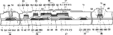
Be used to transmit many grid wirings of signal in upward formation of insulated substrate 10 (Fig. 5 B).Grid wiring comprises: gate line 22, horizontal-extending shown in Fig. 5 A; Grid end 24 is connected to the end of gate line 22, to accept from the signal of outside and this signal is transferred to gate line 22; Gate electrode 26 is connected to gate line 22 as the part of the TFT of projection; And keep electrode (sustain electrode) 27 and keep electrode wires 28, it is parallel to gate line 22.Keep electrode wires 28 horizontal-extendings pass pixel region and be connected to than keep electrode wires 28 wide keep electrode 27.Keep electrode 27 and be overlapped in the drain electrode extension 67 that links to each other with pixel electrode 82 (but is separated by dielectric 30, not shown among Fig. 5 A), keep capacitor with formation, this keeps the electric charge holding capacity of capacitor raising pixel.Keeping electrode 27 can change to some extent with the shape of keeping electrode wires 28 and arrangement, if can be enough high by the overlapping hold facility that produces (sustain capability) between pixel electrode 82 and the gate line 22 certainly, so also can not form and keep electrode 27 and keep electrode wires 28.
Grid wiring is made up of three layers (structural sheets) 22,24,26,27 and 28.Three-decker gate line 22 comprises conductive layer 221,222 and 223.Three-decker layer 24 comprises conductive layer 241,242 and 243.Three-decker layer 26 comprises conductive layer 261,262 and 263.Three-decker layer 27 comprises conductive layer 271,272 and 273.Conductive layer 221,241,261 and 271 is formed by the electric conductive oxidation material, for example tin indium oxide (ITO) or indium zinc oxide (IZO) (hereinafter referred to as " bottom conductive oxide layer ").Conductive layer 222,242,262 and 272 is formed by Ag or Ag alloy.Conductive layer 223,243,263 and 273 forms (hereinafter referred to as " top conductive oxide layer ") by the electric conductive oxidation material such as ITO or IZO.Though not shown among Fig. 5 B, keep electrode wires 28 and also have the three-decker identical with three- decker layer 22,24,26 and 27.Below comprise in the description for the grid wiring of three-decker and keep electrode wires 28.
Three layers (structural sheet) 22,24,26 and 27 26S Proteasome Structure and Function are identical with three-decker layer in the above-mentioned method of making the Ag wiring according to the embodiment of the invention.
Data arrange is formed on impedance contact layer 55,56 and the gate insulator 30.Data arrange comprises: data line 62 vertically shown in Fig. 5 A forms and intersects with definite pixel with gate line 22; Source electrode 65, it is the branch of data line 62 and extends on the impedance contact layer 55; Data end 68, the picture signal that is connected to the end of data line 62 and accepts to come from the outside; Drain electrode 66 separates and formation on impedance contact layer 56 with source electrode 65, assigns to from the groove of gate electrode 26 or TFT, and is relative with source electrode 65; And drain electrode extension 67, its have from drain electrode 66 extend and with keeping electrode 27 overlapping big zone, but separated by dielectric 30 between them.
Data arrange is made up of three layers (structural sheets) 62,65,66,67 and 68.The data line 62 of three-decker comprises conductive layer 621,622 and 623.The source electrode 65 of three-decker comprises conductive layer 651,652 and 653.The drain electrode 66 of three-decker comprises conductive layer 661,662 and 663.Three-decker layer 67 comprises conductive layer 671,672 and 673.Three-decker layer 68 comprises conductive layer 681,682 and 683.Conductive layer 621,651,661,671 and 681 forms (to call " bottom conductive oxide layer " in the following text) by the electric conductive oxidation material such as ITO.Conductive layer 622,652,662,672 and 682 forms (to call " Ag conductive layer " in the following text) by Ag or Ag alloy.Conductive layer 623,653,663,673 and 683 forms (hereinafter referred to as " top conductive oxide layer ") by the electric conductive oxidation material such as ITO.Here and since bottom conductive oxide layer 621,651,661,671 with 681 and top conductive oxide layer 623,653,663,673 and 683 26S Proteasome Structure and Function and grid wiring in identical, so it is not given explanation.
It is overlapping with semiconductor layer 40 that source electrode 65 has a part at least.Drain electrode 66 and source electrode contraposition also are positioned at the top of the part of gate electrode 26, and it is overlapping with semiconductor layer 40 to have a part at least shown in Fig. 5 B.Here, impedance layer 55 and 56 is present between semiconductor layer 40 and the source electrode 65 respectively and between semiconductor layer 40 and the drain electrode 66, to reduce contact impedance therebetween.
Be connected to the auxiliary grid end 84 of grid end 24 and be formed on the passivation layer 70 by contact hole 74 by the auxiliary data end 88 that contact hole 78 is connected to data end 68.Pixel electrode 82, auxiliary grid end 84 and auxiliary data end 88 are formed by ITO.
5A and 5B and Fig. 6 A to 9B specifically describe the manufacture method according to the TFT substrate of the embodiment of the invention below with reference to accompanying drawings.
Shown in Fig. 6 A and 6B, on insulated substrate 10, deposit the conductive layer that forms by the conductive layer that forms such as electric conductive oxidation materials such as ITO or IZO, by Ag successively and by the conductive layer that forms such as electric conductive oxidation materials such as ITO or IZO, form grid three- decker layer 22,24,26,27 and 28 (Fig. 6 B is not shown) thus, it comprises bottom conductive oxide layer 221,241,261 and 271, conductive layer 222,242,262 and 272 and top conductive oxide layer 223,243,263 and 273.
Grid three- decker layer 22,24,26,27 and 28 is by using the method according to the formation tertiary structure layer in the method for embodiment of the invention manufacturing Ag wiring to form.
Next on grid three-decker layer, carry out photoetching.Photoetching treatment uses etchant to be undertaken by wet the quarter.Etchant is identical with the described etchant of Fig. 1 to 4, therefore it will not laid down a definition.
When using etchant according to the embodiment of the invention to carry out etching, because etchant has very high etching selectivity for the three-decker layer and shows outstanding etching uniformity coefficient, just can do not influence three- decker grid wiring 22,24,26,27 and 28 and substrate 10 between the situation of adhesiveness under acquisition have the side profile of better taper acute angle.
Therefore, shown in Fig. 6 A and 6B, formed and comprise gate line 22, gate electrode 26, grid end 24, keep electrode 27 and keep the grid wiring of electrode wires 28.
Next, shown in Fig. 7 A and 7B, by such as chemical vapor deposition (CVD) deposit thickness successively being the gate insulator 30 (also claiming dielectric 30 in this article sometimes), the intrinsic amorphous silicon layer (will form silicon layer 40) that thickness is 500-2000 and the doped amorphous silicon layer (will form impedance contact 55 and 56) that thickness is 300-600 that form by silicon nitride of 1500-5000 .On intrinsic amorphous silicon layer 40 and doped amorphous silicon layer, carry out photoetching,, and on the gate insulator 30 of covering grid electrode 24, form impedance contact layer 55 and 56 with formation island semiconductor layer 40.
Here, because gate insulator 30, intrinsic amorphous silicon layer 40 and doped amorphous silicon layer are to form under about 200 ℃ or higher temperature, so the amorphous ITO that comprises in the grid wiring is converted into crystallization ITO.As a result, improved conductive oxide layer 221,241,261,271,223,243,263 and 273 and Ag conductive layer 222,242,262 and 272 between adhesiveness.
Next, shown in Fig. 8 A and 8B, on the expose portion of gate insulator 30, semiconductor layer 40 and impedance contact layer 55,56, deposit data three- decker layer 62,65,66,67 and 68 successively by sputter, wherein bottom conductive oxide layer 621,651,661,671 and 681 is formed by ITO, Ag conductive layer 622,652,662,672 and 682 is formed by Ag or Ag alloy, and top conductive oxide layer 623,653,663,673 and 683 is formed by ITO.Here, since deposition bottom conductive oxide layer 621,651,661,671 and 681, Ag conductive layer 622,652,662,672 with 682 and the processing of top conductive oxide layer 623,653,663,673 and 683 method and above-mentioned formation grid wiring in deposit bottom conductive oxide layer 221,241,261 and 271, Ag conductive layer 222,242,262 and 272 and the method for top conductive oxide layer 223,243,263 and 273 identical, so no longer provide the explanation of repetition.
On data three-decker layer, carry out photoetching.Photoetching treatment is to use etchant to be undertaken by wet carve.This etchant is identical with the described etchant of Fig. 1 to 4, therefore it will be further described.
When using etchant according to the embodiment of the invention to carry out etching, because etchant has very high etching selectivity and shows etching uniformity coefficient preferably for data three-decker layer, just can do not influence three-decker data arrange 62,65,66,67 and 68 and gate insulator 30 and impedance contact layer 55,56 between the situation of adhesiveness under formation have the side profile of better taper acute angle.
Therefore, formed data arrange 62,65,66,67 and 68, it comprises with gate line 22 data line crossing 62, is connected to data line 62 and extends to source electrode 62 on the gate electrode 26, be connected to the data end 68 of data line 62 ends, separate with source electrode 65 and see and source electrode 65 opposed drain electrode 66 and drain electrode extensions 67 from gate electrode 26, and it has from drain electrode 66 and extends and be overlapped in the big zone that (but being located away from by dielectric 30) keeps electrode 27.
Remove not the part of the doped amorphous silicon layer that is covered by data arrange so that expose semiconductor layer part 40 between impedance contact layer 55 and 56 by etching, data arrange 62,65,66,67 and 68 is separated, but 65 and 66 parts wherein still are retained in the top of gate electrode 26 both sides shown in Fig. 5 B.At this moment, preferably carry out the surface that the oxygen plasma body technology comes the exposed parts of stabilization of semiconductor layer 40.
Next, shown in Fig. 9 A and 9B, formed passivation layer 70 can be single layer structure or the sandwich construction that comprises the organic material with good flatness of the response and photosensitivity.For example, passivation layer 70 can be by the Si:C:O that forms by PECVD, and the insulating material with low-k is perhaps formed by the inorganic material such as SiNx such as Si:O:F.
Next, gate insulator 30 and passivation layer 70 are patterned by photoetching, thereby form the contact hole 74,77 and 78 that exposes grid end 24, drain electrode expansion teat (drain electrode extension) 67 and data end 68.At this moment, when passivation layer 70 when having the organic layer of photosensitivity, contact hole 74,77 and 78 can only form by photoetching.Preferably use gate insulator 30 and passivation layer 70 are had identical optionally etchant and etch process forms contact hole 74,77 and 78.
At last, shown in Fig. 5 A and 5B, deposition ITO layer also carries out photoetching, to form the pixel electrode 82 that is connected to drain electrode 66 by contact hole 77, formation is connected to the auxiliary grid end 84 of grid end 24 by contact hole 74, and forms the auxiliary data end 88 that is connected to data end 68 by contact hole 78.
Though in present embodiment of the present invention, on substrate, formed the grid wiring and the data arrange of the three-decker that comprises bottom conductive oxide layer, Ag conductive layer and top conductive oxide layer, but can have only grid wiring or data arrange to form by three-decker.In addition, though grid wiring and data arrange are to be formed by the three-decker that comprises bottom conductive oxide layer, Ag conductive layer and top conductive oxide layer on substrate, conductive oxide layer also can be formed in the conductive layer of the sandwich construction of Ag conductive layer below or top.
In the foregoing description, formed semiconductor layer and data arrange by using different masks to carry out photoetching, but also can be as described below, form semiconductor layer and data arrange by using single photoresist pattern to carry out photoetching.
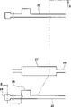
Describe with reference to Figure 10 A to 19B below and use the structure of the unit pixel of the TFT substrate of TFT substrate manufacturing method manufactured according to another embodiment of the present invention.
Figure 10 A shows and uses the layout of the TFT substrate of TFT substrate manufacturing method manufactured according to another embodiment of the present invention, Figure 10 B is the cross-sectional view that intercepts along B-B line shown in Figure 10 A.
In an embodiment of the present invention, at first on insulated substrate 10, form the grid wiring of many transmission signals.This grid wiring comprises: gate line 22, horizontal-extending shown in Figure 10 A; Grid end 24 is connected to the end of gate line 22, is used to receive from the signal of outside and this signal is transferred to gate line 22; Gate electrode 26 is connected to gate line 22 as the part of the TFT of projection; And keep electrode (sustainelectrode) 27 and be parallel to gate line 22 keep electrode wires 28.In Figure 10 A, keep electrode wires 28 horizontal-extendings pass pixel region and be connected to than keep electrode wires 28 wide keep electrode 27.Shown in Figure 10 B, keep electrode 27 parts and be positioned at the part below of the drain electrode extension 67 that (but being separated by the part of the part of dielectric 30, inner silica layer 44 and doped amorphous silicon layer 56) link to each other with pixel electrode 82, keep the electric charge holding capacity that capacitor improves pixel with formation.Keep electrode 27 and can change,, then can not form and keep electrode 27 and keep electrode wires 28 when enough high by the overlapping hold facility that produces between pixel electrode 82 and the gate line 22 with the shape of keeping electrode wires 28 and arrangement.
In the embodiment of the invention shown in Fig. 5 A to 9B, grid wiring is made up of three- decker layer 22,24,26,27 and 28, the conductive layer 222,242,262 that it comprises the bottom conductive oxide layer 221,241,261 and 271 that formed by ITO or IZO, formed by Ag or Ag alloy and 272 and the top conductive oxide layer 223,243,263 and 273 that formed by ITO or IZO.
Data arrange 62,65,66,67 and 68 is formed on impedance contact layer 52,55,56 and 58.Data arrange comprises: data line 62, vertically and with gate line 22 intersect to determine pixel shown in Figure 10 A; Source electrode 65, it is as a branch of data line 62 and extend on the impedance contact layer 55a; Data end 68, the picture signal that is connected to the end of data line 62 and accepts to come from the outside, drain electrode 66, be separated with source electrode 65, be formed on the impedance contact layer 56 and relative with source electrode 65, the part of covering grid electrode 26 simultaneously, it has determined the trench region of TFT; And drain electrode extension 67, it has from drain electrode 66 extensions and is overlapped in the big zone of keeping electrode 27.
Data arrange 62,65,66,67 and 68 is made up of the three-decker layer, and it comprises the conductive layer 621,651,661,671 and 681 (hereinafter referred to as " bottom conductive oxide layer ") that formed by the electric conductive oxidation material, the conductive layer 622,652,662,672 and 682 (to call " Ag conductive layer " in the following text) that is formed by Ag and Ag alloy and the conductive layer 623,653,663,673 and 683 (hereinafter referred to as " top conductive oxide layer ") that is formed by the electric conductive oxidation material.
Simultaneously, except the trench portions of TFT, semiconductor pattern 42,44 and 48 has and data arrange 62,65,66,67 and 68 and the identical shape of impedance contact layer 52,55,56 and 58.That is to say that in the trench portions of TFT, source electrode 65 and drain electrode 66 are separated from one another and also separated from one another with the impedance contact layer 56 under the drain electrode 66 at the impedance contact layer under the source electrode 65 55.But the semiconductor pattern 44 that is used for TFT is continuous in the trench portions of TFT, has formed the groove of TFT thus.
In addition, be connected to the auxiliary grid end 84 of grid end 24 by contact hole 74 and be formed on the passivation layer 70 by the auxiliary data end 88 that contact hole 78 is connected to data end 68.Pixel electrode 82, auxiliary grid end 84 and auxiliary data end 88 are formed by ITO.
10A and 10B and Figure 11 A to 19B describe the manufacture method of TFT substrate according to another embodiment of the present invention below with reference to accompanying drawings.
At first, shown in Figure 11 A and 11B, by the conductive layer 222,242,262 that deposits the bottom conductive oxide layer 221,241,261 and 271 that forms by ITO or IZO in the embodiment of the invention shown in Fig. 5 A to 9B successively, form by Ag or Ag alloy and 272 and form grid three- decker layer 22,24,26,27 and 28 by the top conductive oxide layer 223,243,263 and 273 that ITO or IZO form.
Next, on grid three- decker layer 22,24,26,27 and 28, carry out photoetching.Photoetching treatment is by carrying out the wet quarter of using etchant.Etchant is identical with the described etchant of Fig. 1 to 4, therefore no longer it is illustrated.
Therefore, shown in Figure 11 A and 11B, formed and comprise gate line 22, gate electrode 26, grid end 24, keep electrode 27 and keep the grid wiring of electrode wires 28.
Next, as shown in figure 12, by the chemical vapor deposition (CVD) successive sedimentation thickness doped amorphous silicon layer 50 that for example is 300-600 respectively for the gate insulator 30 that forms by silicon nitride of 1500-5000 , intrinsic amorphous silicon layer 40 that thickness is 500-2000 and thickness.Form data three-decker layer 60 by sputtering on the doped amorphous silicon layer 50, stack gradually the bottom conductive oxide layer 601 that forms by ITO in this layer, the Ag conductive layer 602 that forms by Ag or Ag alloy and the top conductive oxide layer 603 that forms by ITO.Here, the deposition process of data three-decker layer 60 is identical with the data three-decker layer of the embodiment of the invention shown in Fig. 5 A to 9B.
Photoresist layer 110 is coated on the data three-decker layer 60.
With reference to Figure 13 A to Figure 18, light passes mask and projects on the photoresist layer 110 and develop.Form the photoresist pattern 112 and 114 shown in Figure 13 B like this.At this moment, in photoresist pattern 112 and 114, the trench portions of TFT to be formed, promptly be positioned under the photoresist 114 (Figure 13 B) and be positioned at source electrode 65 to be formed and drain electrode 66 to be formed (Figure 16,17 and 18) between the first of amorphous silicon layer 40, covered by photoresist 114, the thickness of photoresist 114 is littler than the thickness of the photoresist 112 that is positioned at data arrange part top (being the second portion of photoresist 112 of the top, zone of data arrange to be formed).Except that the data arrange part of the trench portions of photoresist 114 and photoresist 112, the remainder of photoresist layer 110 (Figure 12) is removed.At this moment, the photoresist layer 114 that remains in the transistorized trench portions of TFT to be formed top with remain in the function that thickness between the photoresist layer 112 of data arrange on partly likens to the photoetching process that will describe after a while and change.The thickness of the first photoresist part 114 preferably less than the thickness of the second photoresist part 112 half (being approximately 8000 in one embodiment), that is to say, less than 4000 .Like this, the thickness of photoresist layer 110 can change in many ways with the variation of position.A kind of mode is to use the incident light quantity of well-known photoetching process change on the different piece of photoresist layer 110.In order to regulate the light quantity of transmission, can form slit or lattice pattern or use semitransparent thin film as the used mask part of photoresist layer 110 one patterned.
At this moment, the gap between the pattern on the line thickness of pattern or the mask between the slit on the mask, i.e. the width of slit is preferably less than the resolution of exposure system.When using semitransparent layer, can use transmittance or thickness to be different from the part of the film of the transmittance of semitransparent layer or thickness, with the transmittance of control mask part when making mask as mask as mask.
In case light projects on the photoresist layer 110 by mask, the polymkeric substance that directly is exposed in photoresist layer 110 parts of light is just decomposed fully.But because it is little to see through the light amount of mask, the polymkeric substance that is arranged in the photoresist 110 under the mask part that is formed with slit pattern or semitransparent layer is not decomposed fully, and the polymkeric substance in the photoresist under the mask light shield layer 110 almost is not decomposed yet.In case photoresist layer 110 is developed, the part of having only polymkeric substance not to be decomposed in the photoresist layer 110 is kept, and it is little that the thickness that has a small amount of light to be transmitted to the part of the photoresist 110 on it does not have light to be transmitted to the thickness of the part on it than those.A small amount of light transmission is on photoresist part 114.At this moment, if the time shutter is long, might the polymkeric substance of photoresist 110 in all microspheres all be decomposed, so should suitably adjust the time shutter.Polymeric material can be novolac resin, and the time shutter (being expressed as energy) can be about 36mmJ.
In one embodiment, but will be exposed by normal masks (it is divided into the part and the complete lighttight part of printing opacity fully) by the photoresist layer that reflow materials is made, this photoresist layer is developed and photoresist layer is refluxed, thereby the part of photoresist layer 114 flow to the zone of no photoetching glue-line 114, has so just formed the photoresist part 114 of thickness less than photoresist part 112." reflux technique " can surpass the photoresist inversion temperature and make photoresist layer flow to trench region downwards and carry out by the heating photoresist layer.Use above-mentioned etchant etching to have the data three-decker layer 60 and the photoresist pattern 114 of top conductive oxide layer 603, Ag conductive layer 602 and bottom conductive oxide layer 601 now.Because the etching process of the etching process of the formation data arrange of this etching process and the embodiment of the invention shown in Fig. 5 A to 9B and formation grid wiring 22,24,26,28 and 29 is roughly the same, so no longer it is illustrated.
Like this, as shown in figure 14, have only 62 and 68 of the three-decker pattern 64 of trench portions to be formed and data line part to be retained.Other parts of data three-decker layer 60 are removed fully.As a result, doped amorphous silicon layer 50 is exposed.Except that source electrode 65 did not separate (promptly limiting) as yet with drain electrode 66, residual three- decker pattern 62,64 was identical with data arrange (shown in Fig. 5 B 62,65,66,67 and 68) with 68 among Figure 14 and Figure 15.
Next, as shown in figure 15, the doped amorphous silicon layer 50 and the intrinsic amorphous silicon layer 40 that expose are done the method at quarter, to remove all parts of these layers except that trench portions (layer 44 among Figure 15) and data arrange part (layer 42 and 48 among Figure 15).Simultaneously, the first 114 of photoresist layer was also by doing method removal at quarter.The result who does the processing at quarter is shown in xsect Figure 15.Preferably, carrying out this etching process makes photoresist pattern 112 and 114, doped amorphous silicon layer 50 and intrinsic amorphous silicon layer 40 by etchings simultaneously and gate insulator 30 is not etched.Especially, to photoresist pattern 112 with 114 to the similar each other situation of the etching selectivity of intrinsic amorphous silicon layer 40 under to carry out etching be preferred.For example, use SF
6Or the mixed gas of HCl or SF
6Or O
2Mixed gas two layers can be etched to similar thickness.When to photoresist pattern 112 when identical with the etching selectivity of intrinsic amorphous silicon layer 40 with 114, the thickness of first 114 is equal to or less than the gross thickness of intrinsic amorphous silicon layer 40 and doped amorphous silicon layer 50.Stop to do quarter in the appropriate time, thereby dielectric layer 30 and ITO layer 643 are in fact done step etching at quarter by this.In one embodiment, the mixed gas that comprises such as SF6 and HCL enters reaction chamber, and applies high-frequency electric field to cause glow discharge plasma to reaction chamber.By being bumped, this plasma and intrinsic amorphous silicon layer and doped amorphous silicon layer do quarter.Like this, as shown in figure 15, after the first 114 of removing trench region, source/drain three-decker pattern 64 is exposed, and behind the doped amorphous silicon layer 50 and intrinsic amorphous silicon layer 40 of removing other parts, gate insulator 30 is exposed.Because the second photoresist part 112 of cover data wiring portion is also etched, the thickness of photoresist part 112 has been reduced the thickness that is equivalent to photoresist part 114 at least.
The residual fraction of lip-deep photoresist layer 110 that is deposited in the source/drain three-decker pattern 64 of trench portions is removed by ashing.
Next, as shown in figure 16, the part of the three-decker pattern 64 of the top conductive oxide layer 643 that comprises trench portions, Ag conductive layer 642 and the bottom conductive oxide layer 641 shown in Figure 15 is removed by for example wet etching, to expose the upper surface of doped amorphous silicon layer 50.In this etching step, used with referring to figs. 1 through 4 described identical etchants.Therefore this etching step is no longer described.
Etched by the impedance contact layer that doped amorphous silicon 50 forms.At this moment, can adopt the method at quarter of doing.Etching gas can be CF
4Potpourri or CF with HCl
4And O
2Potpourri.When using CF
4And O
2The time, the uniform thickness of the semiconductor pattern 44 that is formed by intrinsic amorphous silicon can obtain keeping.At this moment, as shown in figure 16, the part of semiconductor layer 44 is removed, and therefore can reduce the thickness of layer 44 etched part.The second portion 112 of photoresist pattern also can be etched, thereby the thickness of this part photoresist 112 will be reduced.The etching of carrying out should make gate insulator 30 not etched.Special etch mixed gas above-mentioned in this section can reach such effect.Photoresist pattern 112 should be thicker, so that do not exposed at etching second portion 112 back data arranges 62,65,66,67 and 68, this also is preferred.
Like this, source electrode 65 and drain electrode 66 are separated and decide, complete thus data arrange 65 and 66 of having formed, and itself and impedance contact layer 55 and 56 are formed these electrodes.
Next, as shown in figure 17, the second portion 112 of photoresist layer that is deposited in the data arrange part top of structure is removed.
Next, as shown in figure 18, passivation layer 70 is formed on the top of the upper surface of structure.This layer is typically formed by silicon nitride.Shown in Figure 19 A and 19B, on passivation layer 70 and gate insulator 30, carry out photoetching, thereby form contact hole 77,74 and 78, expose drain electrode extension 67, grid end 24 and data end 68.
At last, shown in Figure 10 A and 10B, deposit thickness between 400-500 the ITO layer and it is carried out photoetching, thereby form the pixel electrode 82 that is connected to drain electrode extension 67, be connected to the auxiliary grid end 84 of grid end 24 and be connected to the auxiliary data end 88 of data end 68.
It is desirable to before deposition ITO, use nitrogen to preheat processing, form metal oxide layer to prevent to be exposed on the outer metal level 24,67 and 68 by contact hole 74,77 and 78.
In another embodiment of the present invention, can obtain effect according to the embodiment of the invention, and only use single mask to form data arrange 62,65,66,67 and 68, impedance contact layer 52,55,56 and 58 and semiconductor pattern 42 and 48, wherein drain electrode 66 and source electrode 65 are separated and decide, thereby have simplified manufacture process.
Though in present embodiment of the present invention, adopt comprise bottom conductive oxide layer, Ag conductive layer and top conductive oxide layer three-decker as an example, have only grid wiring or data arrange can have three-decker.In addition, though grid wiring and data arrange form the three-decker that comprises bottom conductive oxide layer, Ag conductive layer and top conductive oxide layer on substrate, conductive oxide layer still can be for being formed on the sandwich construction conductive layer of Ag conductive layer below or top.
Manufacture method according to TFT substrate of the present invention can apply in the colour filter matrix (wherein the TFT matrix is formed on the colored filter for array on color filter, AOC) at an easy rate.
As mentioned above, by using etchant etching to be included on the Ag conductive layer and/or the sandwich construction of the conductive oxide layer under the Ag conductive layer according to the embodiment of the invention, the adhesiveness between sandwich construction and the substrate can be kept, and the conducting wiring of good profile can be obtained to have.In addition, by using etchant etching manufacturing according to the embodiment of the invention to have on the Ag conductive layer and/or the TFT substrate of the sandwich construction of the conductive oxide layer under the Ag conductive layer, can strengthen the adhesiveness between grid wiring and data arrange and the TFT substrate, and improve the profile of grid wiring and data arrange, thereby improve signal characteristic and picture quality.
It will be apparent to one skilled in the art that under the prerequisite of not violating spirit of the present invention and protection domain, foregoing preferred embodiment can have various changes and variation.Therefore, preferred embodiment disclosed in this invention only is used for usually descriptive purposes, and is not to be used to limit the present invention.
Claims (23)
1. etchant, it comprises material, ammonium acetate and the balance of deionized water with molecular formula 1, wherein, described molecular formula 1 is expressed as:
M(OH)
XL
Y ...(1)
Wherein M represents Zn, Sn, Cr, Al, Ba, Fe, Ti, Si or B, and X represents 2 or 3, and L represents H
2O, NH
3, CN, COR or NH
2R, Y represent 0,1,2 or 3, and R represents alkyl.
2. etchant according to claim 1, wherein, the amount of described material in the scope of 0.1-5wt% and the amount of described ammonium acetate in the scope of 0.001-0.1wt%.
3. etchant according to claim 1 and 2 further comprises the phosphoric acid of 60-70wt% scope, the nitric acid of 0.5-5wt% scope and the acetate of 2-10wt% scope.
4. method of making wiring, described method comprises:
Form sandwich construction on substrate, it comprises conductive oxide layer and the Ag conductive layer that is formed by Ag or Ag alloy; And
Use the described sandwich construction of etchant etching, described etchant comprises material, ammonium acetate and the balance of deionized water with molecular formula 1, and wherein, described molecular formula 1 is expressed as:
M(OH)
XL
Y ...(1)
Wherein, M represents Zn, Sn, Cr, Al, Ba, Fe, Ti, Si or B,
X represents 2 or 3, and L represents H
2O, NH
3, CN, COR or NH
2R, Y represent 0,1,2 or 3, and R represents alkyl.
5. method according to claim 4, wherein, described conductive layer and conductive oxide layer that the formation of described sandwich construction is included on the described substrate depositing electrically conductive oxide layer successively, is formed by Ag or Ag alloy.
6. method according to claim 4, wherein, the amount of described material in the scope of 0.1-5wt% and the amount of described ammonium acetate in the scope of 0.001-0.1wt%.
7. according to claim 4 or 6 described methods, further comprise the phosphoric acid of 60-70wt% scope, the nitric acid of 0.5-5wt% scope and the acetate of 2-10wt% scope.
8. method according to claim 4, wherein, described substrate is formed by insulator or semiconductor.
9. method according to claim 4 wherein, is carried out under the described 30-50 of being etched in ℃ the temperature.
10. method according to claim 4, wherein, described etching is undertaken by injection.
11. method according to claim 4, wherein, 30-100 second is carried out in described etching.
12. method according to claim 4, wherein, described each layer that forms described sandwich construction that be etched in upward carries out in the mode of gradation.
13. method according to claim 4, wherein, described conductive oxide layer is formed by tin indium oxide (ITO) or indium zinc oxide (IZO).
14. a method that is used to make thin film transistor (TFT) (TFT) substrate, described method comprises:
On substrate, form the grid sandwich construction that will form grid, comprise conductive oxide layer and the conductive layer that forms by Ag or Ag alloy;
By making described grid sandwich construction one patterned form grid wiring;
On described substrate and grid wiring, form gate insulator and semiconductor layer;
On described semiconductor layer, form the data sandwich construction of the conductive layer comprise conductive oxide layer and to form by Ag or Ag alloy; And
By making described data sandwich construction one patterned form data arrange;
Wherein, the formation of described grid wiring and/or described data arrange comprises uses the etchant that comprises material, ammonium acetate and balance of deionized water with molecular formula 1 to carry out etching, and wherein, described molecular formula 1 is expressed as:
M(OH)
XL
Y ...(1)
M represents Zn, Sn, Cr, Al, Ba, Fe, Ti, Si or B, and X represents 2 or 3, and L represents H
2O, NH
3, CN, COR or NH
2R, Y represent 0,1,2 or 3, and R represents alkyl.
15. method according to claim 14, wherein, conductive layer and conductive oxide layer that the formation of described grid sandwich construction is included on the described substrate depositing electrically conductive oxide layer successively, is formed by Ag or Ag alloy.
16. method according to claim 14, wherein, conductive layer and conductive oxide layer that the formation of described data sandwich construction is included on the described substrate depositing electrically conductive oxide layer successively, is formed by Ag or Ag alloy.
17. method according to claim 14, wherein, the amount of described material in the scope of 0.1-5wt% and the amount of described ammonium acetate in the scope of 0.001-0.1wt%.
18., further comprise the phosphoric acid of 60-70wt% scope, the nitric acid of 0.5-5wt% scope and the acetate of 2-10wt% scope according to claim 14 or 17 described methods.
19. method according to claim 14 wherein, is carried out under the described 30-50 of being etched in ℃ the temperature.
20. method according to claim 14, wherein, described etching is undertaken by injection.
21. method according to claim 14, wherein, 30-100 second is carried out in described etching.
22. method according to claim 14, wherein, described each layer that forms described sandwich construction that be etched in upward carries out in the mode of gradation.
23. method according to claim 14, wherein, described conductive oxide layer is formed by tin indium oxide (ITO) or indium zinc oxide (IZO).
Applications Claiming Priority (2)
| Application Number | Priority Date | Filing Date | Title |
|---|---|---|---|
| KR1020050049453 | 2005-06-09 | ||
| KR1020050049453A KR101124569B1 (en) | 2005-06-09 | 2005-06-09 | Echant and method for fabricating interconnection line and method for fabricating thin film transistor substrate using the same |
Publications (1)
| Publication Number | Publication Date |
|---|---|
| CN1877448A true CN1877448A (en) | 2006-12-13 |
Family
ID=37509918
Family Applications (1)
| Application Number | Title | Priority Date | Filing Date |
|---|---|---|---|
| CNA2006100674071A Pending CN1877448A (en) | 2005-06-09 | 2006-03-27 | Etchant, method for fabricating a wire using the etchant, and method for fabricating a thin film transistor substrate using the etchant |
Country Status (5)
| Country | Link |
|---|---|
| US (2) | US7357878B2 (en) |
| JP (1) | JP4988242B2 (en) |
| KR (1) | KR101124569B1 (en) |
| CN (1) | CN1877448A (en) |
| TW (1) | TWI388062B (en) |
Cited By (3)
| Publication number | Priority date | Publication date | Assignee | Title |
|---|---|---|---|---|
| CN101542692B (en) * | 2007-07-19 | 2011-04-13 | 林纯药工业株式会社 | Etching solution composition |
| CN104659035A (en) * | 2013-11-25 | 2015-05-27 | 乐金显示有限公司 | Array substrate including oxide thin film transistor and method of fabricating the same |
| CN104893728A (en) * | 2015-04-10 | 2015-09-09 | 深圳新宙邦科技股份有限公司 | Low-tension etching solution used for ITO/Ag/ITO film |
Families Citing this family (23)
| Publication number | Priority date | Publication date | Assignee | Title |
|---|---|---|---|---|
| US7288444B2 (en) * | 2001-04-04 | 2007-10-30 | Samsung Sdi Co., Ltd. | Thin film transistor and method of manufacturing the same |
| KR20060097381A (en) * | 2005-03-09 | 2006-09-14 | 삼성전자주식회사 | Thin film transistor substrate and method of manufacturing the same |
| KR100987840B1 (en) * | 2007-04-25 | 2010-10-13 | 주식회사 엘지화학 | Thin film transistor and method for preparing the same |
| KR100982395B1 (en) | 2007-04-25 | 2010-09-14 | 주식회사 엘지화학 | Thin film transistor and method for preparing the same |
| JP2009194351A (en) * | 2007-04-27 | 2009-08-27 | Canon Inc | Thin film transistor and its manufacturing method |
| KR20090095181A (en) * | 2008-03-05 | 2009-09-09 | 삼성전자주식회사 | Etchant composition for a patterned metal layer, method of patterning a conductive layer using the same and method of manufacturing a flat panel display using the same |
| KR101747391B1 (en) * | 2009-07-07 | 2017-06-15 | 엘지디스플레이 주식회사 | Array substrate for liquid crystal display device and methode of fabricating the same |
| CN102655155B (en) * | 2012-02-27 | 2015-03-11 | 京东方科技集团股份有限公司 | Array substrate, manufacturing method and display device thereof |
| KR102290801B1 (en) * | 2013-06-21 | 2021-08-17 | 가부시키가이샤 한도오따이 에네루기 켄큐쇼 | Semiconductor device and manufacturing method thereof |
| US20150069011A1 (en) * | 2013-09-11 | 2015-03-12 | Carestream Health, Inc. | Wet etching patterning compositions and methods |
| KR102091541B1 (en) * | 2014-02-25 | 2020-03-20 | 동우 화인켐 주식회사 | Preparing method for organic light emitting display device |
| KR101972630B1 (en) * | 2015-01-05 | 2019-04-26 | 동우 화인켐 주식회사 | Etching solution composition for silver layer and an display substrate using the same |
| KR20160108944A (en) * | 2015-03-09 | 2016-09-21 | 동우 화인켐 주식회사 | Etching solution composition for silver-containing layer and manufacturing method of an array substrate for display device using the same |
| TWI631205B (en) * | 2015-11-06 | 2018-08-01 | 東友精細化工有限公司 | Etching solution composition for silver layer and an display substrate using the same |
| KR102433385B1 (en) * | 2015-11-10 | 2022-08-17 | 동우 화인켐 주식회사 | Etching solution composition for silver layer and display substrate using the same |
| KR20190058758A (en) | 2017-11-21 | 2019-05-30 | 삼성디스플레이 주식회사 | Etchant and manufacturing method of display device using the same |
| KR102554816B1 (en) | 2018-04-23 | 2023-07-12 | 삼성디스플레이 주식회사 | Echant composition and manufacturing method of metal pattern using the same |
| KR102661845B1 (en) | 2018-10-11 | 2024-04-30 | 삼성디스플레이 주식회사 | Echtant and method for manufacturing display device using the same |
| KR102669119B1 (en) | 2018-11-14 | 2024-05-24 | 삼성디스플레이 주식회사 | Etching composition, method for forming pattern and method for manufacturing a display device using the same |
| US11898081B2 (en) | 2019-11-21 | 2024-02-13 | Tokyo Ohka Kogyo Co., Ltd. | Ruthenium-etching solution, method for manufacturing ruthenium-etching solution, method for processing object to be processed, and method for manufacturing ruthenium-containing wiring |
| JP6895577B2 (en) * | 2019-11-21 | 2021-06-30 | 東京応化工業株式会社 | Etching liquid, manufacturing method of etching liquid, treatment method of object to be treated, and manufacturing method of ruthenium-containing wiring |
| KR102676044B1 (en) | 2020-04-29 | 2024-06-20 | 삼성디스플레이 주식회사 | Etchant and manufacturing method of display device using the same |
| KR102659176B1 (en) | 2020-12-28 | 2024-04-23 | 삼성디스플레이 주식회사 | Etching composition for thin film containing silver, method for forming pattern and method for manufacturing a display device using the same |
Family Cites Families (15)
| Publication number | Priority date | Publication date | Assignee | Title |
|---|---|---|---|---|
| US6132522A (en) * | 1996-07-19 | 2000-10-17 | Cfmt, Inc. | Wet processing methods for the manufacture of electronic components using sequential chemical processing |
| JP2000008184A (en) * | 1998-06-24 | 2000-01-11 | Toppan Printing Co Ltd | Etching of multilayer electrically conductive film |
| US6387600B1 (en) * | 1999-08-25 | 2002-05-14 | Micron Technology, Inc. | Protective layer during lithography and etch |
| JP2002231706A (en) | 2001-02-01 | 2002-08-16 | Matsushita Electric Ind Co Ltd | Etching liquid and method for manufacturing thin film transistor using the same |
| KR100848109B1 (en) | 2001-10-23 | 2008-07-24 | 삼성전자주식회사 | An etchant for a wire, a method for manufacturing the wire and a method for manufacturing a thin film transistor array substrate including the method |
| CN100371809C (en) * | 2001-07-06 | 2008-02-27 | 三星电子株式会社 | An etchant for a wire, a method for manufacturing the wire and a method for manufacturing a thin film transistor array panel including the method |
| KR100840333B1 (en) * | 2001-10-23 | 2008-06-20 | 삼성전자주식회사 | A etchant for wires, a method for manufacturing the wires using the etchant, a thin film transistor array substrate and a method for manufacturing the same including the method |
| KR100415617B1 (en) * | 2001-12-06 | 2004-01-24 | 엘지.필립스 엘시디 주식회사 | Etchant and method of fabricating metal wiring and thin film transistor using the same |
| US20030162398A1 (en) * | 2002-02-11 | 2003-08-28 | Small Robert J. | Catalytic composition for chemical-mechanical polishing, method of using same, and substrate treated with same |
| US20030168431A1 (en) * | 2002-02-25 | 2003-09-11 | Ritdisplay Corporation | Etchant composition for silver alloy |
| KR100853216B1 (en) * | 2002-06-25 | 2008-08-20 | 삼성전자주식회사 | an etchant for a wiring, a method for manufacturing the wiring, a thin film transistor array panel including the wiring, and a method for manufacturing the same including the method |
| JP2004156070A (en) * | 2002-11-01 | 2004-06-03 | Kanto Chem Co Inc | Composition of etchant for multilayer film including transparent electroconductive film |
| JP2004356616A (en) * | 2003-05-28 | 2004-12-16 | Samsung Electronics Co Ltd | Etchant for wiring and method for manufacturing thin film transistor display panel using the same |
| KR100960687B1 (en) * | 2003-06-24 | 2010-06-01 | 엘지디스플레이 주식회사 | An etchant to etching a double layer with Cuor Cu-alloy |
| WO2005022592A2 (en) * | 2003-08-22 | 2005-03-10 | Fujifilm Electronic Materials U.S.A., Inc. | Novel aqueous based metal etchant |
-
2005
- 2005-06-09 KR KR1020050049453A patent/KR101124569B1/en active IP Right Grant
-
2006
- 2006-02-09 US US11/351,015 patent/US7357878B2/en active Active
- 2006-03-16 TW TW095108951A patent/TWI388062B/en active
- 2006-03-27 CN CNA2006100674071A patent/CN1877448A/en active Pending
- 2006-04-25 JP JP2006121189A patent/JP4988242B2/en active Active
-
2008
- 2008-02-21 US US12/035,316 patent/US7955521B2/en active Active
Cited By (4)
| Publication number | Priority date | Publication date | Assignee | Title |
|---|---|---|---|---|
| CN101542692B (en) * | 2007-07-19 | 2011-04-13 | 林纯药工业株式会社 | Etching solution composition |
| CN104659035A (en) * | 2013-11-25 | 2015-05-27 | 乐金显示有限公司 | Array substrate including oxide thin film transistor and method of fabricating the same |
| CN104893728A (en) * | 2015-04-10 | 2015-09-09 | 深圳新宙邦科技股份有限公司 | Low-tension etching solution used for ITO/Ag/ITO film |
| CN104893728B (en) * | 2015-04-10 | 2018-11-27 | 深圳新宙邦科技股份有限公司 | A kind of etching solution of the low-tension for ITO/Ag/ITO film |
Also Published As
| Publication number | Publication date |
|---|---|
| KR101124569B1 (en) | 2012-03-15 |
| JP2006344939A (en) | 2006-12-21 |
| US7955521B2 (en) | 2011-06-07 |
| US20060278606A1 (en) | 2006-12-14 |
| TW200701472A (en) | 2007-01-01 |
| KR20060128210A (en) | 2006-12-14 |
| US7357878B2 (en) | 2008-04-15 |
| TWI388062B (en) | 2013-03-01 |
| US20080142756A1 (en) | 2008-06-19 |
| JP4988242B2 (en) | 2012-08-01 |
Similar Documents
| Publication | Publication Date | Title |
|---|---|---|
| CN1877448A (en) | Etchant, method for fabricating a wire using the etchant, and method for fabricating a thin film transistor substrate using the etchant | |
| US7586554B2 (en) | Liquid crystal display device and dielectric film usable in the liquid crystal display device | |
| CN1773341A (en) | Method of manufacturing flexible display device | |
| KR100433463B1 (en) | Pattern formation method and method of manufacturing display using it | |
| CN100346218C (en) | Thin film transistor array panel and producing method thereof | |
| CN1752852A (en) | The composition and the thin-film transistor display panel manufacture method that are used for stripping photoresist | |
| TWI452445B (en) | Photoresist stripper composition and methods for forming wire structures and for fabricating thin film transistor substrate using composition | |
| CN101079429A (en) | Thin film transistor array substrate and method for fabricating the same | |
| CN1897269A (en) | Wire structure, method of forming wire, thin film transistor substrate, and method of manufacturing thin film transistor substrate | |
| CN1655326A (en) | Method for doping impurities, methods for producing semiconductor device and applied electronic apparatus | |
| CN1917202A (en) | Wire structure, a method for fabricating a wire, a thin film transistor substrate, and a method for fabricating the thin film transistor substrate | |
| CN1875488A (en) | Liquid crystal display device, its manufacturing method, and liquid crystal television receiver | |
| CN1884618A (en) | Etchant, method for fabricating interconnection line using the etchant, and method for fabricating thin film transistor substrate using the etchant | |
| CN1801479A (en) | Method of manufacturing a flexible thin film transistor array panel including plastic substrate | |
| CN1786801A (en) | Thin film transistor array panel and method for manufacturing the same | |
| CN1897270A (en) | Wire structure, method for fabricating wire, thin film transistor substrate, and method for fabricating thin film transistor substrate | |
| CN1945855A (en) | Thin-film transistor, TFT-array substrate, liquid-crystal display device and method of fabricating the same | |
| CN1790750A (en) | Thin film transistor, method of manufacturing the same, display apparatus having the same and method of manufacturing the display apparatus | |
| CN1845341A (en) | Thin film transistor and method of fabricating the same | |
| KR101278477B1 (en) | Metod of fabricating thin film transistor substrate | |
| CN1913146A (en) | Thin film conductor and method of fabrication | |
| CN1551367A (en) | Thin film transistor array substrate and method of fabricating the same | |
| CN1614483A (en) | Method for fabricating liquid crystal display device | |
| CN1655056A (en) | Optic mask and manufacturing method of thin film transistor array panel using the same | |
| CN1714431A (en) | TFT substrate for liquid crystal display apparatus and method of manufacturing the same |
Legal Events
| Date | Code | Title | Description |
|---|---|---|---|
| C06 | Publication | ||
| PB01 | Publication | ||
| C10 | Entry into substantive examination | ||
| SE01 | Entry into force of request for substantive examination | ||
| C12 | Rejection of a patent application after its publication | ||
| RJ01 | Rejection of invention patent application after publication |
Open date: 20061213 |