CN1750737A - Printed circuit board having chip package mounted theron and method of fabricating same - Google Patents
Printed circuit board having chip package mounted theron and method of fabricating same Download PDFInfo
- Publication number
- CN1750737A CN1750737A CNA2005100635320A CN200510063532A CN1750737A CN 1750737 A CN1750737 A CN 1750737A CN A2005100635320 A CNA2005100635320 A CN A2005100635320A CN 200510063532 A CN200510063532 A CN 200510063532A CN 1750737 A CN1750737 A CN 1750737A
- Authority
- CN
- China
- Prior art keywords
- layer
- circuit
- circuit layer
- substrate
- encapsulation module
- Prior art date
- Legal status (The legal status is an assumption and is not a legal conclusion. Google has not performed a legal analysis and makes no representation as to the accuracy of the status listed.)
- Pending
Links
Images


Classifications
-
- H—ELECTRICITY
- H10—SEMICONDUCTOR DEVICES; ELECTRIC SOLID-STATE DEVICES NOT OTHERWISE PROVIDED FOR
- H10W—GENERIC PACKAGES, INTERCONNECTIONS, CONNECTORS OR OTHER CONSTRUCTIONAL DETAILS OF DEVICES COVERED BY CLASS H10
- H10W70/00—Package substrates; Interposers; Redistribution layers [RDL]
- H10W70/60—Insulating or insulated package substrates; Interposers; Redistribution layers
-
- H—ELECTRICITY
- H05—ELECTRIC TECHNIQUES NOT OTHERWISE PROVIDED FOR
- H05K—PRINTED CIRCUITS; CASINGS OR CONSTRUCTIONAL DETAILS OF ELECTRIC APPARATUS; MANUFACTURE OF ASSEMBLAGES OF ELECTRICAL COMPONENTS
- H05K1/00—Printed circuits
- H05K1/18—Printed circuits structurally associated with non-printed electric components
- H05K1/182—Printed circuits structurally associated with non-printed electric components associated with components mounted in printed circuit boards [PCB], e.g. insert-mounted components [IMC]
- H05K1/183—Printed circuits structurally associated with non-printed electric components associated with components mounted in printed circuit boards [PCB], e.g. insert-mounted components [IMC] associated with components mounted in and supported by recessed areas of the PCBs
-
- H—ELECTRICITY
- H05—ELECTRIC TECHNIQUES NOT OTHERWISE PROVIDED FOR
- H05K—PRINTED CIRCUITS; CASINGS OR CONSTRUCTIONAL DETAILS OF ELECTRIC APPARATUS; MANUFACTURE OF ASSEMBLAGES OF ELECTRICAL COMPONENTS
- H05K1/00—Printed circuits
-
- H—ELECTRICITY
- H05—ELECTRIC TECHNIQUES NOT OTHERWISE PROVIDED FOR
- H05K—PRINTED CIRCUITS; CASINGS OR CONSTRUCTIONAL DETAILS OF ELECTRIC APPARATUS; MANUFACTURE OF ASSEMBLAGES OF ELECTRICAL COMPONENTS
- H05K3/00—Apparatus or processes for manufacturing printed circuits
- H05K3/46—Manufacturing multilayer circuits
- H05K3/4697—Manufacturing multilayer circuits having cavities, e.g. for mounting components
-
- H—ELECTRICITY
- H05—ELECTRIC TECHNIQUES NOT OTHERWISE PROVIDED FOR
- H05K—PRINTED CIRCUITS; CASINGS OR CONSTRUCTIONAL DETAILS OF ELECTRIC APPARATUS; MANUFACTURE OF ASSEMBLAGES OF ELECTRICAL COMPONENTS
- H05K2201/00—Indexing scheme relating to printed circuits covered by H05K1/00
- H05K2201/10—Details of components or other objects attached to or integrated in a printed circuit board
- H05K2201/10613—Details of electrical connections of non-printed components, e.g. special leads
- H05K2201/10621—Components characterised by their electrical contacts
- H05K2201/10734—Ball grid array [BGA]; Bump grid array
-
- H—ELECTRICITY
- H05—ELECTRIC TECHNIQUES NOT OTHERWISE PROVIDED FOR
- H05K—PRINTED CIRCUITS; CASINGS OR CONSTRUCTIONAL DETAILS OF ELECTRIC APPARATUS; MANUFACTURE OF ASSEMBLAGES OF ELECTRICAL COMPONENTS
- H05K2203/00—Indexing scheme relating to apparatus or processes for manufacturing printed circuits covered by H05K3/00
- H05K2203/13—Moulding and encapsulation; Deposition techniques; Protective layers
- H05K2203/1377—Protective layers
- H05K2203/1394—Covering open PTHs, e.g. by dry film resist or by metal disc
-
- H—ELECTRICITY
- H05—ELECTRIC TECHNIQUES NOT OTHERWISE PROVIDED FOR
- H05K—PRINTED CIRCUITS; CASINGS OR CONSTRUCTIONAL DETAILS OF ELECTRIC APPARATUS; MANUFACTURE OF ASSEMBLAGES OF ELECTRICAL COMPONENTS
- H05K3/00—Apparatus or processes for manufacturing printed circuits
- H05K3/02—Apparatus or processes for manufacturing printed circuits in which the conductive material is applied to the surface of the insulating support and is thereafter removed from such areas of the surface which are not intended for current conducting or shielding
- H05K3/06—Apparatus or processes for manufacturing printed circuits in which the conductive material is applied to the surface of the insulating support and is thereafter removed from such areas of the surface which are not intended for current conducting or shielding the conductive material being removed chemically or electrolytically, e.g. by photo-etch process
- H05K3/061—Etching masks
- H05K3/062—Etching masks consisting of metals or alloys or metallic inorganic compounds
-
- H—ELECTRICITY
- H05—ELECTRIC TECHNIQUES NOT OTHERWISE PROVIDED FOR
- H05K—PRINTED CIRCUITS; CASINGS OR CONSTRUCTIONAL DETAILS OF ELECTRIC APPARATUS; MANUFACTURE OF ASSEMBLAGES OF ELECTRICAL COMPONENTS
- H05K3/00—Apparatus or processes for manufacturing printed circuits
- H05K3/02—Apparatus or processes for manufacturing printed circuits in which the conductive material is applied to the surface of the insulating support and is thereafter removed from such areas of the surface which are not intended for current conducting or shielding
- H05K3/06—Apparatus or processes for manufacturing printed circuits in which the conductive material is applied to the surface of the insulating support and is thereafter removed from such areas of the surface which are not intended for current conducting or shielding the conductive material being removed chemically or electrolytically, e.g. by photo-etch process
- H05K3/061—Etching masks
- H05K3/064—Photoresists
-
- H—ELECTRICITY
- H05—ELECTRIC TECHNIQUES NOT OTHERWISE PROVIDED FOR
- H05K—PRINTED CIRCUITS; CASINGS OR CONSTRUCTIONAL DETAILS OF ELECTRIC APPARATUS; MANUFACTURE OF ASSEMBLAGES OF ELECTRICAL COMPONENTS
- H05K3/00—Apparatus or processes for manufacturing printed circuits
- H05K3/22—Secondary treatment of printed circuits
- H05K3/24—Reinforcing of the conductive pattern
- H05K3/244—Finish plating of conductors, especially of copper conductors, e.g. for pads or lands
-
- H—ELECTRICITY
- H05—ELECTRIC TECHNIQUES NOT OTHERWISE PROVIDED FOR
- H05K—PRINTED CIRCUITS; CASINGS OR CONSTRUCTIONAL DETAILS OF ELECTRIC APPARATUS; MANUFACTURE OF ASSEMBLAGES OF ELECTRICAL COMPONENTS
- H05K3/00—Apparatus or processes for manufacturing printed circuits
- H05K3/22—Secondary treatment of printed circuits
- H05K3/28—Applying non-metallic protective coatings
-
- H—ELECTRICITY
- H05—ELECTRIC TECHNIQUES NOT OTHERWISE PROVIDED FOR
- H05K—PRINTED CIRCUITS; CASINGS OR CONSTRUCTIONAL DETAILS OF ELECTRIC APPARATUS; MANUFACTURE OF ASSEMBLAGES OF ELECTRICAL COMPONENTS
- H05K3/00—Apparatus or processes for manufacturing printed circuits
- H05K3/46—Manufacturing multilayer circuits
- H05K3/4644—Manufacturing multilayer circuits by building the multilayer layer by layer, i.e. build-up multilayer circuits
- H05K3/4652—Adding a circuit layer by laminating a metal foil or a preformed metal foil pattern
-
- H—ELECTRICITY
- H10—SEMICONDUCTOR DEVICES; ELECTRIC SOLID-STATE DEVICES NOT OTHERWISE PROVIDED FOR
- H10W—GENERIC PACKAGES, INTERCONNECTIONS, CONNECTORS OR OTHER CONSTRUCTIONAL DETAILS OF DEVICES COVERED BY CLASS H10
- H10W90/00—Package configurations
- H10W90/701—Package configurations characterised by the relative positions of pads or connectors relative to package parts
- H10W90/721—Package configurations characterised by the relative positions of pads or connectors relative to package parts of bump connectors
- H10W90/724—Package configurations characterised by the relative positions of pads or connectors relative to package parts of bump connectors between a chip and a stacked insulating package substrate, interposer or RDL
-
- Y—GENERAL TAGGING OF NEW TECHNOLOGICAL DEVELOPMENTS; GENERAL TAGGING OF CROSS-SECTIONAL TECHNOLOGIES SPANNING OVER SEVERAL SECTIONS OF THE IPC; TECHNICAL SUBJECTS COVERED BY FORMER USPC CROSS-REFERENCE ART COLLECTIONS [XRACs] AND DIGESTS
- Y10—TECHNICAL SUBJECTS COVERED BY FORMER USPC
- Y10T—TECHNICAL SUBJECTS COVERED BY FORMER US CLASSIFICATION
- Y10T29/00—Metal working
- Y10T29/49—Method of mechanical manufacture
- Y10T29/49002—Electrical device making
- Y10T29/49117—Conductor or circuit manufacturing
- Y10T29/49124—On flat or curved insulated base, e.g., printed circuit, etc.
- Y10T29/4913—Assembling to base an electrical component, e.g., capacitor, etc.
-
- Y—GENERAL TAGGING OF NEW TECHNOLOGICAL DEVELOPMENTS; GENERAL TAGGING OF CROSS-SECTIONAL TECHNOLOGIES SPANNING OVER SEVERAL SECTIONS OF THE IPC; TECHNICAL SUBJECTS COVERED BY FORMER USPC CROSS-REFERENCE ART COLLECTIONS [XRACs] AND DIGESTS
- Y10—TECHNICAL SUBJECTS COVERED BY FORMER USPC
- Y10T—TECHNICAL SUBJECTS COVERED BY FORMER US CLASSIFICATION
- Y10T29/00—Metal working
- Y10T29/49—Method of mechanical manufacture
- Y10T29/49002—Electrical device making
- Y10T29/49117—Conductor or circuit manufacturing
- Y10T29/49124—On flat or curved insulated base, e.g., printed circuit, etc.
- Y10T29/49155—Manufacturing circuit on or in base
Landscapes
- Engineering & Computer Science (AREA)
- Microelectronics & Electronic Packaging (AREA)
- Manufacturing & Machinery (AREA)
- Production Of Multi-Layered Print Wiring Board (AREA)
- Manufacturing Of Printed Circuit Boards (AREA)
Abstract
Description
技术领域technical field
本发明一般涉及印刷电路板(PB)及其制造方法,更具体地,涉及PCB及其制造方法,其中在多层PCB的内层上形成接触部分,形成沟槽以暴露内层的接触部分,以及将芯片封装模块安装在PCB上,同时倒装(flip-chip)接合到内层暴露的接触部分上。The present invention generally relates to a printed circuit board (PB) and a manufacturing method thereof, and more particularly, to a PCB and a manufacturing method thereof, wherein a contact portion is formed on an inner layer of a multilayer PCB, a groove is formed to expose the contact portion of the inner layer, And the chip package module is mounted on the PCB while flip-chip bonding to the exposed contact portion of the inner layer.
背景技术Background technique
半导体封装的例子有树脂密封封装、TCP封装、玻璃密封封装和金属密封封装。此外,半导体封装分类为TH型,其中穿过PCB形成孔并将针脚插入该孔中,和表面贴装技术(SMT)型,其中根据其安装方法将其贴装在PCB表面上。Examples of semiconductor packages are resin-sealed packages, TCP packages, glass-sealed packages, and metal-sealed packages. Also, semiconductor packages are classified into a TH type in which a hole is formed through the PCB and pins are inserted into the hole, and a surface mount technology (SMT) type in which it is mounted on the surface of the PCB according to its mounting method.
TH型是使用时间最长的典型集成电路(IC)封装,并且代表性的实例包括双列直插式封装(DIP),其中多个针脚从封装两侧直线伸出,和针脚栅格阵列(PGA),其中将针脚排列在大六面体的底面。The TH type is the longest-serving typical integrated circuit (IC) package, and representative examples include the dual in-line package (DIP), in which multiple pins protrude linearly from both sides of the package, and the grid array of pins ( PGA), where the pins are arranged on the base of a large hexahedron.
SMT型是具有下述结构的封装,其中当将被封装芯片电连接到衬底时,不是象将针脚插入孔中并焊接的TH型那样,而是在衬底上获得电连接。The SMT type is a package having a structure in which when a packaged chip is electrically connected to a substrate, the electrical connection is obtained on the substrate, not like the TH type in which pins are inserted into holes and soldered.
相比于TH型,假设采用具有相同尺寸的芯片,SMT型的优点在于由于尺寸小而减小的安装面积、薄且重量轻,以及由于低寄生电容或电感导致操作速度随频率的增加而提高。Compared to TH type, assuming a chip with the same size is used, the SMT type has the advantages of reduced mounting area due to small size, thinness and light weight, and increased operation speed with frequency due to low parasitic capacitance or inductance .
其它优点在于不需要形成孔洞,焊接区域和针脚可以减少,可以获得高密度布线和装配,并且可以降低制造PCB的成本。然而,SMT型的缺点在于难以检测已焊接部分的外观。Other advantages are that holes do not need to be formed, soldering areas and pins can be reduced, high-density wiring and assembly can be achieved, and the cost of manufacturing PCBs can be reduced. However, the SMT type has a disadvantage in that it is difficult to inspect the appearance of the soldered part.
SMT型封装的代表性实例包括四方扁平封装(QFP)、塑料有引线芯片载体(PLCC)和球状栅格阵列(BGA)。Representative examples of SMT-type packages include quad flat pack (QFP), plastic leaded chip carrier (PLCC), and ball grid array (BGA).
同时,在PCB上安装多个元件期间对于PCB的尺寸和厚度存在一些限制。近来,对于携带便利的纤薄移动设备的需求增长,因而,必须将集成和无源元件排列到PC表面上具有限定面积和高度的空间中。Meanwhile, there are some restrictions on the size and thickness of the PCB during mounting of multiple components on the PCB. Recently, the demand for slim mobile devices that are easy to carry has increased, and thus, it is necessary to arrange integrated and passive components into a space with a limited area and height on the surface of the PC.
可以制造薄芯片来满足这种要求。不过,这样会发生层间的加工问题和信号干扰问题。Thin chips can be fabricated to meet this requirement. However, this creates processing problems between layers and signal interference problems.
换言之,将多层集成电路芯片集成到一个传统集成电路芯片封装模块中。此时,集成电路芯片必须非常薄以便将多层芯片插入到具有限定厚度的封装中。然而,由于集成电路芯片非常薄,因此难以处理发生在集成电路芯片之间的芯片和信号干扰问题。In other words, the multi-layer integrated circuit chip is integrated into a conventional integrated circuit chip package module. At this time, the integrated circuit chip must be very thin in order to insert the multilayer chip into a package with a defined thickness. However, since the integrated circuit chips are very thin, it is difficult to deal with chip and signal interference problems that occur between the integrated circuit chips.
同时,一种在PCB中嵌入集成电路芯片的技术被提出以补偿不足的空间。Meanwhile, a technology of embedding integrated circuit chips in PCBs was proposed to compensate for the insufficient space.
对于上述技术,日本专利特开No.11-274734公开了一种电子电路设备,其具有作为芯层的电路衬底、安装在电路衬底上的电子元件、形成在电路衬底上的绝缘层和形成在绝缘层上电路。As for the above technology, Japanese Patent Laid-Open No. 11-274734 discloses an electronic circuit device having a circuit substrate as a core layer, electronic components mounted on the circuit substrate, an insulating layer formed on the circuit substrate and form circuits on the insulating layer.
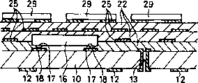
图1为其上安装有芯片的传统PCB的截面图。FIG. 1 is a cross-sectional view of a conventional PCB on which a chip is mounted.
参照图1,在其上安装有芯片的传统PCB中,电路衬底10被用作芯层,并且在电路衬底的上和下面形成电路图案12、18。Referring to FIG. 1, in a conventional PCB on which chips are mounted, a
穿过电路衬底10形成通孔13以相互连接内、外电路。将芯片16倒装接合到电路衬底10上从而安装在其上。形成在集成电路芯片16的焊垫上的焊接凸块17被连接到电路衬底10上的焊环18上。Via
此外,将多个绝缘层22层叠到电路衬底10上,并且在每个绝缘层22上形成电路图案25。Furthermore, a plurality of
在此阶段,将集成电路芯片29安装到绝缘层22的最外层22的外表面上,并将其连接到位于最外绝缘层22表面上的线路图案上。At this stage, an integrated
然而,在将集成电路芯片嵌入PCB的传统技术中,难以形成散热通道,因而很难将该技术应用到产生大量热的集成电路芯片中。However, in the conventional technique of embedding an integrated circuit chip in a PCB, it is difficult to form a heat dissipation channel, and thus it is difficult to apply the technique to an integrated circuit chip that generates a large amount of heat.
此外,由于必须将PCB制造期间产生的灰尘控制到与半导体制造期间相同的水平,因此必须新建清洁室或必须严密控制灰尘水平,这是不希望的。Furthermore, since the dust generated during PCB manufacturing has to be controlled to the same level as during semiconductor manufacturing, it is not desirable that new clean rooms have to be built or dust levels have to be tightly controlled.
发明内容Contents of the invention
因此,牢记现有技术中存在的上述缺点完成本发明,并且本发明的目的在于提供PCB及其制造方法。在该方法中,在PCB中形成在其上将要安装芯片封装模块的接触部分,进行层的层叠使得形成在衬底内层上的接触部分被暴露出来,并且将芯片封装模块倒装接合到内层的接触部分,从而将厚的芯片封装模块安装到在衬底表面具有限定高度的空间中。Therefore, the present invention has been accomplished keeping in mind the above-mentioned disadvantages existing in the prior art, and an object of the present invention is to provide a PCB and a manufacturing method thereof. In this method, a contact portion on which a chip package module is to be mounted is formed in the PCB, layer lamination is performed so that the contact portion formed on the inner layer of the substrate is exposed, and the chip package module is flip-chip bonded to the inner layer. The contact portion of the layer, so that a thick chip package module is mounted in a space with a defined height on the surface of the substrate.
可以通过提供其上安装有芯片封装模块的PCB来达到上述目的,PCB包括具有形成在其上面的多个电接触部分并且作为芯层的衬底。将芯片封装模块安装到衬底上,并且芯片封装模块具有连接到所述电接触部分的凸块。将绝缘层层叠到衬底上,并且绝缘层具有其中将安装芯片封装模块的孔。The above objects can be achieved by providing a PCB on which the chip package module is mounted, the PCB including a substrate having a plurality of electrical contact portions formed thereon and serving as a core layer. A chip package module is mounted on the substrate, and the chip package module has bumps connected to the electrical contact portions. An insulating layer is laminated on the substrate, and has a hole in which the chip package module is to be mounted.
此外,本发明提供一种制造其上安装有芯片封装模块的PCB的方法。该方法包括第一步骤,形成第一抗蚀剂以在衬底一面的第一电路层的上面形成电接触部分;第二步骤,将第一光敏物质涂覆到衬底的第一电路层上,以在第一电路层上形成第一电路图案,并且除去第一光敏物质;第三步骤,在衬底上层叠绝缘层和第二电路层,并且穿过一部分绝缘层形成其中将安装芯片封装模块的孔;第四步骤,涂覆第二光敏物质以在第二电路层上形成第二电路图案,并且在其上形成有第一抗蚀剂的暴露的衬底第一电路层上形成电接触部分;和第五步骤,安装芯片封装模块从而将芯片封装模块连接到形成在暴露的衬底第一电路层上的电接触部分。Furthermore, the present invention provides a method of manufacturing a PCB on which a chip package module is mounted. The method includes a first step of forming a first resist to form an electrical contact portion on the first circuit layer on one side of the substrate; a second step of coating a first photosensitive substance on the first circuit layer of the substrate , to form the first circuit pattern on the first circuit layer, and remove the first photosensitive substance; the third step is to laminate the insulating layer and the second circuit layer on the substrate, and form a package through a part of the insulating layer where the chip will be mounted. The hole of the module; the fourth step, coating the second photosensitive substance to form a second circuit pattern on the second circuit layer, and forming an electrical pattern on the exposed first circuit layer of the substrate with the first resist formed thereon. a contact portion; and a fifth step, mounting the chip package module to connect the chip package module to the electrical contact portion formed on the exposed first circuit layer of the substrate.
此外,本发明提供一种制造其上安装有芯片封装模块的PCB的方法。该方法包括第一步骤,层叠绝缘层和第一电路层到其上形成有第一电路图案的衬底一面上的第二电路层的上面;第二步骤,除去层叠在衬底上的、位置对应于将安装芯片封装模块的区域的绝缘层部分和第一电路层;第三步骤,在内层和外层涂覆光敏物质,以便光敏物质紧密附着到内层和外层,并且在光敏物质上形成第二电路图案以形成电接触部分和在外层上形成第三电路图案;第四步骤,使用形成在光敏物质上的第二电路图案进行蚀刻工艺,以在外层上形成第三电路图案和在内层上形成电接触部分;以及第五步骤,安装芯片封装模块从而将芯片封装模块连接到形成在暴露的衬底第二电路层上的电接触部分。Furthermore, the present invention provides a method of manufacturing a PCB on which a chip package module is mounted. The method includes a first step of laminating an insulating layer and a first circuit layer on top of a second circuit layer on one side of a substrate on which a first circuit pattern is formed; Corresponding to the insulating layer part and the first circuit layer of the area where the chip package module will be installed; the third step is to coat the photosensitive substance on the inner layer and the outer layer so that the photosensitive substance is closely attached to the inner layer and the outer layer, and the photosensitive substance Forming a second circuit pattern on the upper layer to form an electrical contact portion and forming a third circuit pattern on the outer layer; a fourth step, performing an etching process using the second circuit pattern formed on the photosensitive material to form a third circuit pattern and the outer layer forming an electrical contact portion on the inner layer; and a fifth step, mounting the chip package module to connect the chip package module to the electrical contact portion formed on the exposed second circuit layer of the substrate.
此外,本发明提供一种制造其上安装有芯片封装模块的PCB的方法。该方法包括第一步骤,在衬底的第一电路层上形成包括将被连接到芯片封装模块的电接触部分的第一电路图案;第二步骤,将绝缘层和第二电路层层叠到其上形成有第一电路图案的衬底一面的第一电路层的上面;第三步骤,除去层叠在衬底上的、位置对应于将安装芯片封装模块的区域的绝缘层部分和第二电路层;和第四步骤,安装芯片封装模块从而将芯片封装模块连接到形成在暴露的衬底第一电路层上的电接触部分。Furthermore, the present invention provides a method of manufacturing a PCB on which a chip package module is mounted. The method includes a first step of forming a first circuit pattern including an electrical contact portion to be connected to a chip package module on a first circuit layer of a substrate; a second step of laminating an insulating layer and a second circuit layer to it Above the first circuit layer on the side of the substrate on which the first circuit pattern is formed; the third step is to remove the insulating layer part and the second circuit layer stacked on the substrate and corresponding to the area where the chip package module will be mounted and a fourth step of mounting the chip package module so as to connect the chip package module to the electrical contacts formed on the exposed first circuit layer of the substrate.
此外,本发明提供一种制造其上安装有芯片封装模块的PCB的方法。该方法包括第一步骤,在衬底的第一电路层上形成包括将被连接到芯片封装模块的电接触部分的第一电路图案;第二步骤,用抗蚀剂包围电接触部分;第三步骤,层叠穿过其中形成孔的绝缘层,从而将芯片封装模块安装其中,同时将芯片封装模块连接到电接触部分,并层叠第二电路层到绝缘层上;第四步骤,层叠光敏物质到第二电路层上,在光敏物质上形成第二电路图案,其中位置对应于孔的部分光敏物质被除去,并且蚀刻所得衬底以在第二电路层上形成第三电路图案;和第五步骤,安装芯片封装模块从而将芯片封装模块连接到形成在暴露的衬底第一电路层上的电接触部分。Furthermore, the present invention provides a method of manufacturing a PCB on which a chip package module is mounted. The method includes a first step of forming a first circuit pattern including an electrical contact portion to be connected to a chip package module on a first circuit layer of a substrate; a second step of surrounding the electrical contact portion with a resist; third step, laminating the insulating layer through which a hole is formed, thereby mounting the chip package module therein, simultaneously connecting the chip package module to the electrical contact portion, and laminating the second circuit layer on the insulating layer; the fourth step, laminating the photosensitive substance on the On the second circuit layer, forming a second circuit pattern on the photosensitive substance, wherein a part of the photosensitive substance whose position corresponds to the hole is removed, and etching the resulting substrate to form a third circuit pattern on the second circuit layer; and a fifth step and mounting the chip package module to connect the chip package module to electrical contacts formed on the exposed first circuit layer of the substrate.
附图说明Description of drawings
由结合附图的以下详细描述可以更清楚地理解本发明的上述和其他目的、特征和其他优点。The above and other objects, features and other advantages of the present invention can be more clearly understood from the following detailed description in conjunction with the accompanying drawings.
图1为其上安装有芯片的传统PCB的截面图;Fig. 1 is a cross-sectional view of a traditional PCB on which a chip is installed;
图2为根据本发明的第一实施方案的其上安装有芯片封装模块的PCB的截面图;2 is a cross-sectional view of a PCB on which a chip packaging module is mounted according to a first embodiment of the present invention;
图3a-3p为示出根据本发明的第一实施方案制造其上安装有芯片封装模块的PCB的截面图;3a-3p are cross-sectional views illustrating the manufacture of a PCB on which a chip packaging module is mounted according to a first embodiment of the present invention;
图4a-4q为示出根据本发明的第二实施方案制造其上安装有芯片封装模块的PCB的截面图;4a-4q are cross-sectional views illustrating the manufacture of a PCB on which a chip packaging module is mounted according to a second embodiment of the present invention;
图5a-5k为示出根据本发明的第三实施方案制造其上安装有芯片封装模块的PCB的截面图;5a-5k are cross-sectional views illustrating the manufacture of a PCB on which a chip packaging module is mounted according to a third embodiment of the present invention;
图6a-6l为示出根据本发明的第四实施方案制造其上安装有芯片封装模块的PCB的截面图;6a-6l are cross-sectional views illustrating the manufacture of a PCB on which a chip packaging module is mounted according to a fourth embodiment of the present invention;
图7a-7l为示出根据本发明的第五实施方案制造其上安装有芯片封装模块的PCB的截面图;7a-7l are cross-sectional views illustrating the manufacture of a PCB on which a chip packaging module is mounted according to a fifth embodiment of the present invention;
图8a-8m为示出根据本发明的第六实施方案制造其上安装有芯片封装模块的PCB的截面图;8a-8m are cross-sectional views illustrating the manufacture of a PCB on which a chip packaging module is mounted according to a sixth embodiment of the present invention;
图9a-9d为示出根据本发明的第七实施方案制造其上安装有芯片封装模块的PCB的截面图。9a-9d are cross-sectional views illustrating the fabrication of a PCB on which a chip package module is mounted according to a seventh embodiment of the present invention.
具体实施方式Detailed ways
以下,将参照图2-9d给出对本发明的详细描述。Hereinafter, a detailed description of the present invention will be given with reference to FIGS. 2-9d.
图2为根据本发明的第一实施方案的、其上安装有芯片封装模块的PCB的截面图。2 is a cross-sectional view of a PCB on which a chip package module is mounted according to a first embodiment of the present invention.
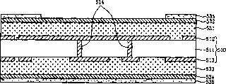
参照图2,根据本发明的第一实施方案的、其上安装有芯片封装模块的PCB包括作为芯层的覆铜层压板210,层叠在覆铜层压板210上的多个绝缘层231、233,多个电路层232、234,涂覆在外电路层232、234和暴露的内电路层212上的阻焊膜240、241,芯片封装模块250,和插入在芯片封装模块250的凸块242和内电路层212的接触部分之间的导电材料242。Referring to FIG. 2, a PCB on which a chip package module is mounted according to a first embodiment of the present invention includes a copper clad laminate 210 as a core layer, a plurality of insulating layers 231, 233 stacked on the copper clad laminate 210 , a plurality of circuit layers 232, 234, solder resist films 240, 241 coated on the outer circuit layers 232, 234 and the exposed inner circuit layer 212, a chip packaging module 250, and bumps 242 and 242 inserted into the chip packaging module 250 and Conductive material 242 between contact portions of inner circuit layer 212 .
覆铜层压板210由绝缘材料制成,并包括具有预定厚度的绝缘层211和位于绝缘层211的两面并具有电路图案的铜箔层211、213。The copper clad laminate 210 is made of insulating material, and includes an insulating layer 211 having a predetermined thickness and copper foil layers 211 , 213 located on both sides of the insulating layer 211 and having circuit patterns.
在此,接触部分形成在绝缘层211的一面上的铜箔层211上,芯片封装模块250的凸块251能被倒装接合到该接触部分上。该接触部分通过通孔214电连接到其它部分213。Here, a contact portion to which the bump 251 of the chip package module 250 can be flip-chip bonded is formed on the copper foil layer 211 on one side of the insulating layer 211 . The contact portion is electrically connected to the other portion 213 through the via hole 214 .
另外,在层叠在覆铜层压板211上面的绝缘层231上形成尺寸对应于芯片封装模块250的沟槽,从而将芯片封装模块250倒装接合到形成在内电路层212中的接触部分上。此外,暴露出内电路层212的接触部分。In addition, a groove having a size corresponding to the chip package module 250 is formed on the insulating layer 231 laminated on the copper clad laminate 211 , thereby flip-chip bonding the chip package module 250 to a contact portion formed in the inner circuit layer 212 . In addition, contact portions of the inner circuit layer 212 are exposed.
芯片封装模块250通过沟槽使用贴在接触部分上的凸块来倒装接合接触部分,从而被安装在PCB上。The chip package module 250 is mounted on the PCB by flip-chip bonding the contact portions through the grooves using bumps attached to the contact portions.
在此阶段,可应用导电材料242以便改善芯片封装模块250的凸块251和接触部分之间的粘结强度。At this stage, the conductive material 242 may be applied in order to improve the bonding strength between the bump 251 and the contact portion of the chip package module 250 .
此外,可在外电路层232和暴露的内部电路层212上涂覆阻焊剂。In addition, solder resist may be coated on the outer circuit layer 232 and the exposed inner circuit layer 212 .
同样,如图2所示,通过采用引线框架,侧壁连接是可行的,因而可以确保用于信号连接的多通道。Also, as shown in Fig. 2, by using a lead frame, side wall connections are possible, thereby ensuring multiple channels for signal connections.
图3a-3p为示出根据本发明的第一实施方案制造其上安装有芯片封装模块的PCB的截面图。3a-3p are cross-sectional views illustrating the manufacture of a PCB on which a chip package module is mounted according to a first embodiment of the present invention.
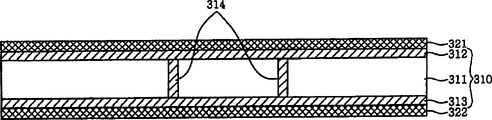
参照图3a,提供了作为芯层的电路衬底310。该电路衬底310由绝缘材料制成,并且包括具有预定厚度的绝缘层311,和位于绝缘层311的上下两面的铜箔层312、313。此外,穿过电路衬底310形成多个通孔314以相互连接电路衬底的两面上的电路。Referring to FIG. 3a, a
参照图3b和3c,光敏物质321、322被涂覆到电路衬底310的铜箔层312、313上。接着,通过曝光和显影工艺有选择地除去上层光敏物质321以暴露未除去的部分铜箔层312,从而形成在其上安装有芯片封装模块的部分。该光刻工艺可被分为照相工艺和丝网印刷工艺。使用其上印刷有电路图案的布线图膜,将照相工艺分为用干膜作为光敏材料的D/F工艺和用光敏液体的光敏液体工艺。Referring to FIGS. 3 b and 3 c ,
参照图3d,能够在使用金或镍的铜蚀刻工艺期间被用作电阻的抗蚀剂323被涂覆在铜箔层暴露部分上,从而在使用金或镍进行铜蚀刻工艺时防止铜箔层被蚀刻,从而提供电连接到待安装芯片封装模块。此时,优选通过镀覆工艺来形成抗蚀剂323。Referring to FIG. 3d, a resist 323 that can be used as a resistor during a copper etching process using gold or nickel is coated on the exposed portion of the copper foil layer, thereby preventing the copper foil layer from are etched to provide electrical connections to the chip package modules to be mounted. At this time, the resist 323 is preferably formed through a plating process.
参照图3e,使用剥除工艺从铜箔层312、313的两面除去光敏物质321、322,并且进一步涂覆光敏物质324、325来形成电路,如图3f所示。Referring to FIG. 3e, the
此时,位置对应于其中将安装芯片封装模块的区域的部分光敏物质324、325未被蚀刻。然而,其下的铜箔层将被蚀刻的剩余部分被曝光和显影以暴露出将被蚀刻的部分铜箔层,如图3g所示。At this time, portions of the photosensitive substances 324, 325 whose positions correspond to the regions where the chip packaging module will be mounted are not etched. However, the remaining portion of the underlying copper foil layer to be etched is exposed and developed to expose the portion of the copper foil layer to be etched, as shown in Figure 3g.
如图3h所示,在使用光敏物质324、325的电路图案作为抗蚀剂形成铜箔的电路图案之后,剥除作为抗蚀剂的光敏物质324、325以完全形成铜箔的电路图案。此时,不可除去抗蚀剂323。As shown in FIG. 3h, after forming the circuit pattern of the copper foil using the circuit pattern of the photosensitive substance 324, 325 as a resist, the photosensitive substance 324, 325 as the resist is stripped to completely form the circuit pattern of the copper foil. At this time, the resist 323 cannot be removed.
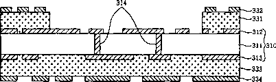
接着,在如图3i所示进行蚀刻工艺从而在内层上形成电路之后,通过剥除工艺除去光敏物质324、325,并且进一步层叠多个绝缘层331、333和电路层332、334。Next, after performing an etching process as shown in FIG. 3i to form a circuit on the inner layer, the photosensitive substances 324, 325 are removed by a stripping process, and a plurality of insulating
如图3j所示,为了除去位置对应于其中将安装芯片封装模块的区域的部分绝缘层331,通过使用激光或等离子体的工艺除去位于该部分绝缘层331上的铜箔。As shown in FIG. 3j , in order to remove a portion of the insulating
接着,在如图3k所示,除去位置对应于其中将安装芯片封装模块的区域的部分铜箔之后,通过能够除去绝缘层331的激光或等离子体工艺除去位置也对应于其中将安装芯片封装模块的区域的部分绝缘层331。此时,如果需要,优选控制绝缘层的去除从而防止所得衬底被过度移除。另外,优选待除去的绝缘层的材料不同于不可除去的绝缘层的材料,从而防止不可被除去的绝缘层被蚀刻。Next, as shown in FIG. 3k, after removing a portion of the copper foil whose position corresponds to the area where the chip package module will be installed, the position also corresponds to where the chip package module will be installed by removing the insulating
如图3l所示,涂覆光敏材料335、336以在最外层332、334上形成电路。As shown in FIG. 31, a photosensitive material 335,336 is applied to form a circuit on the outermost layer 332,334.
如图3m所示,将光敏材料335、336曝光和显影以在其上形成电路图案。此时,移除位置对应于其中将安装芯片封装模块的区域的部分光敏材料335、336,以便通过铜蚀刻工艺来去除位置对应于其中将安装芯片封装模块的区域的内层312的暴露的铜箔部分。As shown in FIG. 3m, the
如图3n所示,使用作为抗蚀剂的光敏材料335、336的电路图案和抗蚀剂323,在外电路层332、334和暴露的内部铜箔层312上形成线路图案。换言之,通过蚀刻工艺在所得衬底表面和内层铜箔312、332、334上形成电路。A circuit pattern is formed on the outer circuit layers 332, 334 and the exposed inner
如图3o所示,在通过剥除工艺彻底除去光敏材料335、336之后,将芯片封装模块安装在衬底内层表面上。当必须除去形成在内层上的抗蚀剂323时,必须通过抗蚀剂剥除工艺进行移除,如图3p所示。然而,如果抗蚀剂是通过镀金形成,则优选不除去抗蚀剂。As shown in FIG. 3o, after the
图4a-4q为示出根据本发明的第二实施方案制造其上安装有芯片封装模块的PCB的截面图。4a-4q are cross-sectional views illustrating the manufacture of a PCB on which a chip package module is mounted according to a second embodiment of the present invention.
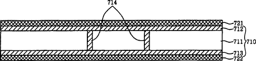
参照图4a,提供作为芯层的电路衬底410。该电路衬底410由绝缘材料制成,并且包括具有预定厚度的绝缘层411,和位于绝缘层411的上下两面的铜箔层412、413。此外,穿过电路衬底410形成多个通孔414以相互连接电路衬底的两面上的电路。Referring to FIG. 4a, a
参照图4b和4c,光敏物质421、422被涂覆到电路衬底410的铜箔层412、413上。接着,通过曝光和显影工艺有选择地除去上层光敏物质421、422以暴露将不被除去的上面的部分铜箔层412,从而形成在其上安装有芯片封装模块的部分。Referring to FIGS. 4 b and 4 c ,
参照图4d,能够在使用金或镍的铜蚀刻工艺中被用作电阻的抗蚀剂423被涂覆在铜箔层暴露部分上,从而在使用金或镍进行铜蚀刻工艺时防止铜箔层被蚀刻,从而提供电连接到待安装芯片封装模块。此时,优选通过镀覆工艺来形成抗蚀剂423。Referring to FIG. 4d, a resist 423 that can be used as a resistor in a copper etching process using gold or nickel is coated on the exposed portion of the copper foil layer, thereby preventing the copper foil layer from are etched to provide electrical connections to the chip package modules to be mounted. At this time, the resist 423 is preferably formed through a plating process.
参照图4e,使用剥除工艺从铜箔层412、413的两面除去光敏物质421、422,并且进一步涂覆光敏物质424、425来形成电路,如图4f所示。Referring to FIG. 4e, the
在此阶段,位置对应于其中将安装芯片封装模块的区域的部分光敏物质424、425未被蚀刻。然而,其下的铜箔层将被蚀刻的剩余部分被曝光和显影以暴露出将被蚀刻的部分铜箔层,如图4g所示。At this stage, portions of the
如图4h所示,在使用光敏物质424、425的电路图案作为抗蚀剂形成铜箔的电路图案之后,剥除作为抗蚀剂的光敏物质424、425以完全形成铜箔的电路图案。As shown in FIG. 4h, after forming the circuit pattern of the copper foil using the circuit pattern of the
接着,在如图4i所示进行蚀刻工艺从而在内层上形成电路之后,通过剥除工艺除去光敏物质424、425,并且进一步层叠多个绝缘层431、433和电路层432、434。Next, after performing an etching process as shown in FIG. 4i to form a circuit on the inner layer, the
如图4j所示,为了除去位置对应于其中将安装芯片封装模块的区域的部分绝缘层431,通过使用激光或等离子体的工艺除去位于该部分绝缘层431上的铜箔。As shown in FIG. 4j , in order to remove a portion of the insulating
接着,在如图4k所示,除去位置对应于其中将安装芯片封装模块的区域的部分铜箔之后,通过能够除去绝缘层431的激光或等离子体工艺除去位置也对应于其中将安装芯片封装模块的区域的部分绝缘层431。在此阶段,如果需要,优选控制绝缘层的去除从而防止所得衬底被过度移除。另外,优选待除去的绝缘层的材料不同于不可除去的绝缘层的材料,从而防止不可被除去的绝缘层被蚀刻。Next, as shown in FIG. 4k, after removing a portion of the copper foil whose position corresponds to the area where the chip package module will be installed, the position also corresponds to where the chip package module will be installed by removing the insulating
如图4l所示,涂覆光敏材料435、436以在最外层432、434上形成电路。A photosensitive material 435,436 is applied to form circuits on the outermost layers 432,434, as shown in FIG. 41.
如图4m所示,将光敏材料435、436曝光和显影以在其上形成电路图案。此时,不除去位置对应于其中将安装芯片封装模块的区域的部分光敏材料435、436。As shown in FIG. 4m, the
如图4n所示,将抗蚀剂437、438涂覆在使用曝光和显影工艺形成在光敏材料435、436上的电路图案上。在此阶段,优选通过镀覆工艺来进行抗蚀剂437、438的涂覆。As shown in Figure 4n, a resist 437, 438 is coated over the circuit pattern formed on the
如图4o所示,除去光敏材料435、436,从而通过使用抗蚀剂437、438的电路图案作为抗蚀剂在铜箔上形成线路图案。As shown in FIG. 4o, the
如图4p所示,在通过剥除工艺除去光敏材料435、436之后,采用抗蚀剂437、438作为抗蚀剂,通过蚀刻工艺在所得衬底表面和内层铜箔412、413、432、434上形成电路。As shown in Figure 4p, after the
如图4q所示,在通过剥除工艺彻底除去抗蚀剂437、438之后,将芯片封装模块安装在衬底内层表面上。如图4q所示,当必须除去形成在内层上的抗蚀剂423时,必须通过抗蚀剂剥除工艺进行移除。然而,如果抗蚀剂是通过镀金形成,则优选不除去抗蚀剂。As shown in FIG. 4q, after the resists 437, 438 are completely removed by a stripping process, the chip package module is mounted on the inner surface of the substrate. As shown in FIG. 4q, when the resist 423 formed on the inner layer must be removed, it must be removed through a resist stripping process. However, if the resist is formed by gold plating, it is preferable not to remove the resist.
图5a-5k为示出根据本发明的第三实施方案制造其上安装有芯片封装模块的PCB的截面图。5a-5k are cross-sectional views illustrating the manufacture of a PCB on which a chip package module is mounted according to a third embodiment of the present invention.
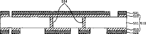
参照图5a,提供作为芯层的电路衬底510。该电路衬底510由绝缘材料制成,并且包括具有预定厚度的绝缘层511,和位于绝缘层511的上下两面的铜箔层512、513。此外,穿过电路衬底510形成多个通孔514以相互连接电路衬底的两面上的电路。Referring to FIG. 5a, a
参照图5b和5c,光敏物质521、522被涂覆到电路衬底510的铜箔层512、513上。接着,通过光刻工艺在位置对应于为安装芯片封装模块的区域的部分光敏物质521、522上形成电路图案,并且使用光敏物质521、522作为抗蚀剂在铜箔层512、513上形成另一电路图案。Referring to FIGS. 5 b and 5 c ,
如图5d所示,通过剥除工艺除去光敏物质521、522,并且如图5e所示,进一步形成多个绝缘层531、533和电路层532、534。As shown in FIG. 5d, the
如图5f所示,为了除去位置对应于其中将安装芯片封装模块的区域的部分绝缘层531,将光敏物质535、536涂覆到最外层532、534上。As shown in Fig. 5f, in order to remove part of the insulating
如图5g所示,为了除去位置对应于其中将安装芯片封装模块的区域的部分绝缘层531,将光敏物质535、536曝光和显影以除去其位置对应于其中将安装芯片封装模块的区域的部分。接着进行蚀刻工艺以除去位置对应于其中将安装芯片封装模块的区域的最外层的部分铜箔层532。As shown in Figure 5g, in order to remove the part of the insulating
在完成光敏物质531的功能之后,如图5h所示,通过剥除工艺除去光敏物质。接着,通过能够使用激光或等离子体除去绝缘层531的工艺,除去位置对应于其中将安装芯片封装模块的区域的部分绝缘层531。此外,将光敏材料537、538涂覆到所得衬底的表面以在外层上形成电路。After completing the function of the
如图5i所示,通过曝光和显影工艺在光敏材料537、538上形成电路。此时,在曝光工艺中,可以使用传播路径非常直的辐射,如UV辐射、X射线或激光来硬化位置对应于其中不安装芯片封装模块的区域的部分光敏材料537、538。As shown in Figure 5i, circuits are formed on the photosensitive materials 537, 538 by exposure and development processes. At this time, in the exposure process, radiation with a very straight propagation path, such as UV radiation, X-ray or laser, may be used to harden the portion of the photosensitive material 537, 538 corresponding to the area where the chip package module is not installed.
同样,如图5j所示,采用光敏材料537、538作为抗蚀剂,通过蚀刻工艺来同时蚀刻在所得衬底表面的铜箔532和其上将安装芯片封装模块的内层铜箔512。Similarly, as shown in FIG. 5j , using photosensitive materials 537 and 538 as resists, the
如图5k所示,在通过剥除工艺彻底除去光敏材料之后,在衬底内层表面上安装芯片封装模块。As shown in FIG. 5k, after the photosensitive material is completely removed by a stripping process, a chip package module is installed on the inner surface of the substrate.
图6a-6l为示出根据本发明的第四实施方案制造其上安装有芯片封装模块的PCB的截面图。6a-6l are cross-sectional views illustrating the fabrication of a PCB on which a chip package module is mounted according to a fourth embodiment of the present invention.
参照图6a,提供作为芯层的电路衬底610。该电路衬底610由绝缘材料制成,并且包括具有预定厚度的绝缘层611,和位于绝缘层611的上下两面的铜箔层612、613。此外,穿过电路衬底610形成多个通孔614以相互连接电路衬底的两面上的电路。Referring to FIG. 6a, a
参照图6b-6d,光敏物质621、622被涂覆到电路衬底610的铜箔层612、613上。接着,通过光刻工艺在光敏物质621、622上形成电路图案,并且随后使用光敏物质621、622作为抗蚀剂在铜箔层612、613上形成另一电路图案。从而,在位置对应于其中将安装芯片封装模块的区域的部分内层612、613上和内层的其它部分上形成电路图案。Referring to FIGS. 6b-6d ,
如图6e所示,通过剥除工艺除去光敏物质621、622,并且如图6f所示,进一步形成多个绝缘层631、633和电路层632、634。As shown in FIG. 6e, the
如图6g所示,为了除去位置对应于其中将安装芯片封装模块的区域的部分绝缘层631,将光敏物质635、636涂覆到最外层632、634上。As shown in Fig. 6g, in order to remove a part of the insulating
如图6h所示,为了除去位置对应于其中将安装芯片封装模块的区域的部分绝缘层631,将光敏物质635曝光和显影,以除去其位置对应于其中将安装芯片封装模块的区域的部分。接着,进行蚀刻工艺以除去位置对应于其中将安装芯片封装模块的区域的最外层的部分铜箔层632。As shown in FIG. 6h, in order to remove part of the insulating
在完成光敏物质635的功能之后,如图6i所示,通过剥除工艺除去光敏物质。接着,如图6j所示,通过能够使用激光或等离子体除去衬底的绝缘层的工艺,除去位置对应于其中将安装芯片封装模块的区域的部分绝缘层631。After completing the function of the
如图6k所示,将光敏材料637、638涂覆到所得衬底表面上,并且随后进行曝光和显影工艺以在外层上形成电路图案。由于已经在其上将安装芯片封装模块的内层612上形成了电路图案,因此电路图案形成在其上不安装芯片封装模块的部分外层上。此时,在曝光工艺中,可以使用传播路径非常直的辐射,如UV辐射、X射线或激光来硬化位置对应于其中铜箔不可被除去的区域的部分光敏材料637、638。As shown in Figure 6k, a
如图6l所示,在通过采用光敏材料637、638作为抗蚀剂的蚀刻工艺来蚀刻所得衬底表面上的铜箔632,并且通过剥除工艺彻底除去光敏材料之后,将芯片封装模块安装到衬底内层表面上。As shown in FIG. 6l, after etching the
图7a-7l为示出根据本发明的第五实施方案制造其上安装有芯片封装模块的PCB的截面图。7a-7l are cross-sectional views illustrating the fabrication of a PCB on which a chip package module is mounted according to a fifth embodiment of the present invention.
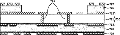
参照图7a,提供作为芯层的电路衬底710。该电路衬底710由绝缘材料制成,并且包括具有预定厚度的绝缘层711,和位于绝缘层711的上下两面的铜箔层712、713。此外,穿过电路衬底710形成多个通孔714以相互连接电路衬底的两面上的电路。Referring to FIG. 7a, a
参照图7b-7d,光敏物质721、722被涂覆到电路衬底710的铜箔层712、713上。接着,通过光刻工艺在光敏物质721、722上形成电路图案,并且随后使用光敏物质721、722作为抗蚀剂在铜箔层712、713上形成另一电路图案。从而,在位置对应于其中将安装芯片封装模块的区域的部分内层712、713上和内层的其它部分上形成电路图案。Referring to FIGS. 7b-7d ,
如图7e所示,通过剥除工艺除去光敏物质721、722。As shown in FIG. 7e, the
如图7f所示,涂覆光敏物质723、724以获得抗蚀剂725的选择性涂覆。A
如图7g所示,将光敏物质723曝光和显影,以暴露其上将涂覆抗蚀剂725的部分。As shown in Figure 7g, the
如图7h所示,涂覆抗蚀剂725之后,通过剥除工艺除去光敏物质723、724。在此阶段,优选使用镀覆工艺来进行抗蚀剂725的涂覆。As shown in FIG. 7h, after coating the resist 725, the
如图7i所示,进一步形成多个绝缘层726、728和电路层727、729。在此,其中将安装芯片封装模块的部分绝缘层726已被除去,并且保留位置对应于绝缘层部分的部分铜箔层727。因此,不需要蚀刻该部分绝缘层726来将芯片封装模块安装到衬底中。As shown in FIG. 7i, a plurality of insulating
如图7j所示,将光敏物质730、731涂覆到最外层727、729上以在最外层727上形成电路图案。As shown in FIG. 7j , a
如图7k所示,将光敏物质730曝光和显影以除去其位置对应于最外层727的电路图案的部分,从而在最外层727上形成电路图案。在此阶段,彻底除去位置对应于其中将安装芯片封装模块的区域的部分光敏物质730。As shown in FIG. 7k , the
此外,使用光敏物质730作为抗蚀剂进行蚀刻工艺以除去位置对应于光敏物质730的电路图案的最外层的部分铜箔层727。In addition, an etching process is performed using the
在完成光敏物质730的功能之后,如图7l所示,通过剥除工艺除去光敏物质。从而,可以将芯片封装模块安装到衬底内层表面上。After the function of the
图8a-8m为示出根据本发明的第六实施方案制造其上安装有芯片封装模块的PCB的截面图。8a-8m are cross-sectional views illustrating the fabrication of a PCB on which a chip package module is mounted according to a sixth embodiment of the present invention.
参照图8a,提供作为芯层的电路衬底810。该电路衬底810由绝缘材料制成,并且包括具有预定厚度的绝缘层811,和位于绝缘层811的上下两面的铜箔层812、813。此外,穿过电路衬底810形成多个通孔814以相互连接电路衬底的两面上的电路。Referring to FIG. 8a, a
参照图8b-8d,光敏物质821、822被涂覆到电路衬底810的铜箔层812、813上。接着,通过光刻工艺在光敏物质821、822上形成电路图案,并且随后使用光敏物质821、822作为抗蚀剂在铜箔层812、813上形成另一电路图案。从而,在位置对应于其中将安装芯片封装模块的区域的部分内层812、813上和内层其它部分上形成电路图案。Referring to FIGS. 8 b - 8 d ,
如图8e所示,通过剥除工艺除去光敏物质821、822。As shown in FIG. 8e, the
如图8f所示,涂覆光敏物质823、824以获得抗蚀剂825的选择性涂覆。A
如图8g所示,将光敏物质823曝光和显影,以暴露其上将涂覆抗蚀剂825的部分。As shown in Figure 8g, the
如图8h所示,涂覆抗蚀剂825之后,通过剥除工艺除去光敏物质823、824。在此阶段,优选使用镀覆工艺来进行抗蚀剂825的涂覆。As shown in FIG. 8h, after coating the resist 825, the
如图8i所示,进一步层叠多个绝缘层826、827。在此,其中将安装芯片封装模块的部分绝缘层826已被除去。因此,不需要蚀刻该部分绝缘层826来将芯片封装模块安装到衬底中。As shown in FIG. 8i, a plurality of insulating
如图8j所示,进行无电镀和电镀铜工艺来形成镀覆层828、829。As shown in Figure 8j, electroless plating and electroplating copper processes are performed to form plated
如图8k所示,将光敏物质830、831涂覆到最外层828、829上以在最外层828、829上形成电路图案。As shown in FIG. 8k , a
如图8l所示,将光敏物质830曝光和显影以除去其位置对应于镀覆层的电路图案的部分,从而在镀覆层828、829上形成电路图案。此时,彻底除去位置对应于其中将安装芯片封装模块的区域的部分光敏物质830。As shown in FIG. 81 , the
此外,使用光敏物质830作为抗蚀剂进行蚀刻工艺以除去位置对应于光敏物质830的电路图案的最外层的部分铜箔层828。In addition, an etching process is performed using the
在完成光敏物质830的功能之后,如图8m所示,通过剥除工艺除去光敏物质。从而,可以将芯片封装模块安装到衬底内层表面上。After completing the function of the
同时,可以在本发明的所有上述实施方案中进行图9a-9d的工艺。At the same time, the process of Figures 9a-9d can be carried out in all the above-described embodiments of the invention.
图9a-9d为示出根据本发明的第七实施方案制造其上安装有芯片封装模块的PCB的截面图。9a-9d are cross-sectional views illustrating the fabrication of a PCB on which a chip package module is mounted according to a seventh embodiment of the present invention.
参照图9a,将阻焊油墨940涂覆到PCB的一整面上,从中根据前述实施方案的方法除去其中将安装芯片封装模块的部分绝缘层931。Referring to FIG. 9a, solder resist
参照图9b,由涂覆到PCB上的阻焊油墨形成的阻焊层940在其位置对应于芯片封装模块的焊料951处被除去。Referring to FIG. 9b, a solder resist
如图9c所示,可以将导电材料或非导电材料242涂覆到通过去除部分PCB阻焊层940而部分暴露的铜箔层912上,从而防止铜箔层氧化和改善安装在PCB上的元件和铜箔层之间的粘结强度。在此阶段,优选通过镀金来涂覆材料。As shown in Figure 9c, a conductive material or a non-conductive material 242 can be applied to the
如图9d所示,采用倒装芯片方法将芯片封装模块安装到PCB上。As shown in Figure 9d, the chip package module is mounted on the PCB using the flip-chip method.
已经以示例的方式描述了本发明PCB的制造,并且应该理解所用术语的目的是描述而不是限制。可以依据以上教导对本发明进行多种改进和变化。因此,应该理解在所附权利要求的范围内,本发明可以不同于所具体描述的方式实施。The fabrication of the PCB of the present invention has been described by way of example and it is to be understood that the terminology used is for the purpose of description and not limitation. Many modifications and variations of the present invention are possible in light of the above teachings. It is therefore to be understood that within the scope of the appended claims, the invention may be practiced otherwise than as specifically described.
如上所述,本发明的优点在于由于将成品芯片封装模块安装在PCB上,因此降低了所需的洁净程度,消除了对额外设备和成本的要求。As mentioned above, the advantage of the present invention is that since the finished chip package module is mounted on the PCB, the degree of cleanliness required is reduced, eliminating the need for additional equipment and costs.
本发明的另一优点在于由于可以将芯片安置到更接近电源层,因此可以降低由干扰导致产生的噪声。Another advantage of the present invention is that the noise caused by interference can be reduced because the chip can be placed closer to the power plane.
本发明的又一优点在于由于使用了引线框架,通过封装的侧壁以及通过封装的底面进行连接是可行的,因而可以为信号连接提供多条通道。A further advantage of the present invention is that due to the use of a lead frame, connections are possible through the side walls of the package as well as through the bottom surface of the package, thereby providing multiple channels for signal connections.
Claims (21)
Applications Claiming Priority (2)
| Application Number | Priority Date | Filing Date | Title |
|---|---|---|---|
| KR1020040074872A KR20060026130A (en) | 2004-09-18 | 2004-09-18 | Printed circuit board mounting chip package and manufacturing method |
| KR1020040074872 | 2004-09-18 |
Publications (1)
| Publication Number | Publication Date |
|---|---|
| CN1750737A true CN1750737A (en) | 2006-03-22 |
Family
ID=36073070
Family Applications (1)
| Application Number | Title | Priority Date | Filing Date |
|---|---|---|---|
| CNA2005100635320A Pending CN1750737A (en) | 2004-09-18 | 2005-04-08 | Printed circuit board having chip package mounted theron and method of fabricating same |
Country Status (3)
| Country | Link |
|---|---|
| US (3) | US7506437B2 (en) |
| KR (1) | KR20060026130A (en) |
| CN (1) | CN1750737A (en) |
Cited By (11)
| Publication number | Priority date | Publication date | Assignee | Title |
|---|---|---|---|---|
| CN101170878B (en) * | 2006-10-27 | 2010-06-16 | 三星电机株式会社 | Method for manufacturing print circuit board |
| CN102931297A (en) * | 2012-11-16 | 2013-02-13 | 映瑞光电科技(上海)有限公司 | LED (Light-Emitting Diode) chip and manufacturing method of LED chip |
| CN103582280A (en) * | 2012-07-20 | 2014-02-12 | 鸿富锦精密工业(深圳)有限公司 | Circuit board device |
| CN103889169A (en) * | 2012-12-22 | 2014-06-25 | 宏启胜精密电子(秦皇岛)有限公司 | Circuit board and manufacturing method thereof |
| CN105304604A (en) * | 2015-10-09 | 2016-02-03 | 株洲宏达天成微波有限公司 | Multi-layer bonding method for multi-pad chip bonding |
| CN106057766A (en) * | 2015-04-13 | 2016-10-26 | 爱思开海力士有限公司 | Substrates, semiconductor packages including same, and electronic systems including semiconductor packages |
| CN106169445A (en) * | 2015-05-22 | 2016-11-30 | 艾马克科技公司 | In order to manufacture, there is multilayer film electrically-conductive backing plate and the method for structural semiconductor encapsulation |
| CN106257968A (en) * | 2015-06-18 | 2016-12-28 | 三星电机株式会社 | Printed circuit board and manufacturing methods |
| CN110785025A (en) * | 2019-11-08 | 2020-02-11 | 生益电子股份有限公司 | PCB manufacturing method and PCB |
| CN115767887A (en) * | 2022-11-09 | 2023-03-07 | 希烽光电科技(南京)有限公司 | Interconnection structure of PCB board and chip, preparation method of interconnection structure and optical module |
| CN120072792A (en) * | 2025-04-25 | 2025-05-30 | 广东风华芯电科技股份有限公司 | Semiconductor packaging substrate and preparation method thereof |
Families Citing this family (29)
| Publication number | Priority date | Publication date | Assignee | Title |
|---|---|---|---|---|
| TWI278501B (en) * | 1999-08-25 | 2007-04-11 | Hitachi Chemical Co Ltd | Adhesive film for connecting wiring terminals |
| JP4196901B2 (en) * | 2004-08-11 | 2008-12-17 | ソニー株式会社 | Electronic circuit equipment |
| KR100639676B1 (en) * | 2004-09-21 | 2006-10-30 | 삼성전자주식회사 | Photolithography Equipment Control System and Control Method for Semiconductor Manufacturing |
| US7420282B2 (en) * | 2004-10-18 | 2008-09-02 | Sharp Kabushiki Kaisha | Connection structure for connecting semiconductor element and wiring board, and semiconductor device |
| US7511228B2 (en) * | 2005-09-14 | 2009-03-31 | Schmartboard, Inc. | Printed circuit board |
| KR100805092B1 (en) * | 2006-05-10 | 2008-02-21 | 주식회사 네패스 | Stacked Multichip Package and Manufacturing Method Thereof |
| KR100819278B1 (en) * | 2006-11-22 | 2008-04-02 | 삼성전자주식회사 | Printed Circuit Board and Manufacturing Method Thereof |
| KR100840790B1 (en) | 2006-11-29 | 2008-06-23 | 삼성전자주식회사 | Semiconductor module and manufacturing method thereof |
| US9084377B2 (en) * | 2007-03-30 | 2015-07-14 | Stats Chippac Ltd. | Integrated circuit package system with mounting features for clearance |
| TWI353661B (en) * | 2007-04-09 | 2011-12-01 | Unimicron Technology Corp | Circuit board structure capable of embedding semic |
| KR20100017408A (en) * | 2007-05-29 | 2010-02-16 | 오컴 포트폴리오 엘엘씨 | Electronic assemblies without solder and methods for their manufacture |
| KR100971294B1 (en) * | 2008-05-08 | 2010-07-20 | 삼성전기주식회사 | Semiconductor plastic package and manufacturing method thereof |
| US20090260862A1 (en) * | 2008-04-16 | 2009-10-22 | Andrew Yaung | Circuit modification device for printed circuit boards |
| JP2012009828A (en) * | 2010-05-26 | 2012-01-12 | Jtekt Corp | Multilayer circuit board |
| KR101167802B1 (en) * | 2010-12-27 | 2012-07-25 | 삼성전기주식회사 | circuit board and method for manufacturing the same |
| KR101225663B1 (en) * | 2011-05-13 | 2013-01-23 | 전자부품연구원 | Chip embedded substrate manufacturing method |
| US9230899B2 (en) * | 2011-09-30 | 2016-01-05 | Unimicron Technology Corporation | Packaging substrate having a holder, method of fabricating the packaging substrate, package structure having a holder, and method of fabricating the package structure |
| KR20130064477A (en) * | 2011-12-08 | 2013-06-18 | 삼성전자주식회사 | Printed circuit board(pcb) comprising one-layer wire pattern |
| US9219029B2 (en) * | 2011-12-15 | 2015-12-22 | Stats Chippac Ltd. | Integrated circuit packaging system with terminals and method of manufacture thereof |
| US8623711B2 (en) | 2011-12-15 | 2014-01-07 | Stats Chippac Ltd. | Integrated circuit packaging system with package-on-package and method of manufacture thereof |
| US8629567B2 (en) | 2011-12-15 | 2014-01-14 | Stats Chippac Ltd. | Integrated circuit packaging system with contacts and method of manufacture thereof |
| KR101326999B1 (en) | 2012-03-07 | 2013-11-13 | 엘지이노텍 주식회사 | The printed circuit board and the method for manufacturing the same |
| KR102192356B1 (en) * | 2013-07-29 | 2020-12-18 | 삼성전자주식회사 | Semiconductor Packages |
| KR102268781B1 (en) | 2014-11-12 | 2021-06-28 | 삼성전자주식회사 | Printed circuit board and method for manufacturing the same |
| KR20160099381A (en) * | 2015-02-12 | 2016-08-22 | 삼성전기주식회사 | Printed circuit board and method of mamufacturing the same |
| WO2016209244A1 (en) | 2015-06-25 | 2016-12-29 | Intel Corporation | Integrated circuit structures with recessed conductive contacts for package on package |
| EP3314648A4 (en) * | 2015-06-25 | 2019-01-09 | Intel Corporation | INTEGRATED CIRCUIT STRUCTURES WITH INTERPOSITION ELEMENTS HAVING EVIDENCE |
| CN110769598B (en) * | 2018-07-27 | 2021-11-16 | 宏启胜精密电子(秦皇岛)有限公司 | Embedded circuit board and manufacturing method thereof |
| CN116031630A (en) * | 2021-10-25 | 2023-04-28 | 深南电路股份有限公司 | Antenna module, preparation method of antenna module and terminal |
Family Cites Families (8)
| Publication number | Priority date | Publication date | Assignee | Title |
|---|---|---|---|---|
| JPS61296800A (en) * | 1985-06-25 | 1986-12-27 | 日本電気株式会社 | Electrode for altering design |
| CN1094717C (en) * | 1995-11-16 | 2002-11-20 | 松下电器产业株式会社 | PC board and fixing body thereof |
| KR100388770B1 (en) | 1998-08-13 | 2003-06-25 | 히다치 가세고교 가부시끼가이샤 | Adhesive for Bonding Circuit Members, Circuit Board, and Method of Producing the Same |
| TW399309B (en) * | 1998-09-30 | 2000-07-21 | World Wiser Electronics Inc | Cavity-down package structure with thermal via |
| US6611635B1 (en) * | 1998-10-09 | 2003-08-26 | Fujitsu Limited | Opto-electronic substrates with electrical and optical interconnections and methods for making |
| US6271127B1 (en) * | 1999-06-10 | 2001-08-07 | Conexant Systems, Inc. | Method for dual damascene process using electron beam and ion implantation cure methods for low dielectric constant materials |
| JP2002062308A (en) | 2000-08-15 | 2002-02-28 | Toyota Motor Corp | Collision type determination device |
| US6603915B2 (en) * | 2001-02-05 | 2003-08-05 | Fujitsu Limited | Interposer and method for producing a light-guiding structure |
-
2004
- 2004-09-18 KR KR1020040074872A patent/KR20060026130A/en not_active Ceased
-
2005
- 2005-04-08 CN CNA2005100635320A patent/CN1750737A/en active Pending
- 2005-05-13 US US11/128,852 patent/US7506437B2/en not_active Expired - Fee Related
-
2009
- 2009-02-09 US US12/367,738 patent/US20090152233A1/en not_active Abandoned
- 2009-02-09 US US12/367,768 patent/US20090147488A1/en not_active Abandoned
Cited By (13)
| Publication number | Priority date | Publication date | Assignee | Title |
|---|---|---|---|---|
| CN101170878B (en) * | 2006-10-27 | 2010-06-16 | 三星电机株式会社 | Method for manufacturing print circuit board |
| CN103582280B (en) * | 2012-07-20 | 2017-10-03 | 鸿富锦精密工业(深圳)有限公司 | Circuit board arrangement |
| CN103582280A (en) * | 2012-07-20 | 2014-02-12 | 鸿富锦精密工业(深圳)有限公司 | Circuit board device |
| CN102931297A (en) * | 2012-11-16 | 2013-02-13 | 映瑞光电科技(上海)有限公司 | LED (Light-Emitting Diode) chip and manufacturing method of LED chip |
| CN102931297B (en) * | 2012-11-16 | 2015-06-24 | 映瑞光电科技(上海)有限公司 | LED (Light-Emitting Diode) chip and manufacturing method of LED chip |
| CN103889169A (en) * | 2012-12-22 | 2014-06-25 | 宏启胜精密电子(秦皇岛)有限公司 | Circuit board and manufacturing method thereof |
| CN106057766A (en) * | 2015-04-13 | 2016-10-26 | 爱思开海力士有限公司 | Substrates, semiconductor packages including same, and electronic systems including semiconductor packages |
| CN106169445A (en) * | 2015-05-22 | 2016-11-30 | 艾马克科技公司 | In order to manufacture, there is multilayer film electrically-conductive backing plate and the method for structural semiconductor encapsulation |
| CN106257968A (en) * | 2015-06-18 | 2016-12-28 | 三星电机株式会社 | Printed circuit board and manufacturing methods |
| CN105304604A (en) * | 2015-10-09 | 2016-02-03 | 株洲宏达天成微波有限公司 | Multi-layer bonding method for multi-pad chip bonding |
| CN110785025A (en) * | 2019-11-08 | 2020-02-11 | 生益电子股份有限公司 | PCB manufacturing method and PCB |
| CN115767887A (en) * | 2022-11-09 | 2023-03-07 | 希烽光电科技(南京)有限公司 | Interconnection structure of PCB board and chip, preparation method of interconnection structure and optical module |
| CN120072792A (en) * | 2025-04-25 | 2025-05-30 | 广东风华芯电科技股份有限公司 | Semiconductor packaging substrate and preparation method thereof |
Also Published As
| Publication number | Publication date |
|---|---|
| KR20060026130A (en) | 2006-03-23 |
| US20090147488A1 (en) | 2009-06-11 |
| US20060060960A1 (en) | 2006-03-23 |
| US20090152233A1 (en) | 2009-06-18 |
| US7506437B2 (en) | 2009-03-24 |
Similar Documents
| Publication | Publication Date | Title |
|---|---|---|
| CN1750737A (en) | Printed circuit board having chip package mounted theron and method of fabricating same | |
| CN1290389C (en) | Circuit-board having internal electronic element and making method thereof | |
| CN1251560C (en) | Part built-in module and manufacturing method thereof | |
| CN1189068C (en) | Multilayer printed circuit board and manufacturing method thereof | |
| CN1138302C (en) | Manufacturing method of semiconductor device and packaging of semiconductor device | |
| CN1275307C (en) | Wiring basilar plate with position information | |
| CN1428829A (en) | Method for mfg. semiconductor assembly | |
| CN1497717A (en) | Circuit device and manufacturing method thereof | |
| CN1956183A (en) | Electronic part built-in substrate and manufacturing method thereof | |
| CN1525544A (en) | Packaging substrate manufactured by leadless electroplating process and manufacturing method thereof | |
| CN1790684A (en) | Ball grid array substrate having window and method of fabricating same | |
| CN101064294A (en) | Circuit device and method for manufacturing circuit device | |
| CN1705104A (en) | Circuit device and manufacturing method thereof | |
| CN1392611A (en) | Semiconductor device and its producing method | |
| CN1705108A (en) | Circuit device and manufacturing method thereof | |
| CN1798478A (en) | Printed circuit board including embedded chips and method of fabricating the same | |
| CN1519920A (en) | Semiconductor device and method for manufacturing semiconductor device | |
| CN1444269A (en) | Multi-layer semiconductor device and its mfg. method | |
| CN1798479A (en) | Printed circuit board including embedded chips and method of fabricating the same | |
| CN1722935A (en) | Method of fabricating PCB including embedded passive chip | |
| CN1343089A (en) | Printed circuit board with channel and manufacturing method thereof | |
| CN1258784C (en) | Stacked ceramic electronic device, composite electronic device, and method for manufacturing a stacked ceramic electronic device | |
| CN1320846C (en) | Circuit board and its manufacturing method | |
| CN1805657A (en) | Wired circuit board | |
| CN1577840A (en) | Stack package of semiconductor device |
Legal Events
| Date | Code | Title | Description |
|---|---|---|---|
| C06 | Publication | ||
| PB01 | Publication | ||
| C10 | Entry into substantive examination | ||
| SE01 | Entry into force of request for substantive examination | ||
| C02 | Deemed withdrawal of patent application after publication (patent law 2001) | ||
| WD01 | Invention patent application deemed withdrawn after publication |