CN1685774A - Flexible circuit with electrostatic damage limiting feature - Google Patents
Flexible circuit with electrostatic damage limiting feature Download PDFInfo
- Publication number
- CN1685774A CN1685774A CNA038227762A CN03822776A CN1685774A CN 1685774 A CN1685774 A CN 1685774A CN A038227762 A CNA038227762 A CN A038227762A CN 03822776 A CN03822776 A CN 03822776A CN 1685774 A CN1685774 A CN 1685774A
- Authority
- CN
- China
- Prior art keywords
- circuit
- flexible circuit
- conductive polymer
- cylinder
- band
- Prior art date
- Legal status (The legal status is an assumption and is not a legal conclusion. Google has not performed a legal analysis and makes no representation as to the accuracy of the status listed.)
- Pending
Links
- 229920001940 conductive polymer Polymers 0.000 claims abstract description 51
- 239000011248 coating agent Substances 0.000 claims abstract description 23
- 238000000576 coating method Methods 0.000 claims abstract description 23
- 239000000758 substrate Substances 0.000 claims abstract description 15
- 239000004642 Polyimide Substances 0.000 claims abstract description 5
- 229920001721 polyimide Polymers 0.000 claims abstract description 5
- 239000000203 mixture Substances 0.000 claims description 26
- 239000000463 material Substances 0.000 claims description 21
- 238000000034 method Methods 0.000 claims description 16
- 238000007639 printing Methods 0.000 claims description 9
- 238000005516 engineering process Methods 0.000 claims description 8
- 229920001467 poly(styrenesulfonates) Polymers 0.000 claims description 7
- 229960002796 polystyrene sulfonate Drugs 0.000 claims description 7
- 239000011970 polystyrene sulfonate Substances 0.000 claims description 7
- 238000012545 processing Methods 0.000 claims description 6
- XKRFYHLGVUSROY-UHFFFAOYSA-N Argon Chemical compound [Ar] XKRFYHLGVUSROY-UHFFFAOYSA-N 0.000 claims description 4
- IJGRMHOSHXDMSA-UHFFFAOYSA-N Atomic nitrogen Chemical compound N#N IJGRMHOSHXDMSA-UHFFFAOYSA-N 0.000 claims description 4
- PXHVJJICTQNCMI-UHFFFAOYSA-N Nickel Chemical compound [Ni] PXHVJJICTQNCMI-UHFFFAOYSA-N 0.000 claims description 4
- 229920002120 photoresistant polymer Polymers 0.000 claims description 4
- 238000009832 plasma treatment Methods 0.000 claims description 4
- 230000001681 protective effect Effects 0.000 claims description 4
- XLYOFNOQVPJJNP-UHFFFAOYSA-N water Substances O XLYOFNOQVPJJNP-UHFFFAOYSA-N 0.000 claims description 4
- NIXOWILDQLNWCW-UHFFFAOYSA-N acrylic acid group Chemical group C(C=C)(=O)O NIXOWILDQLNWCW-UHFFFAOYSA-N 0.000 claims description 3
- 230000003247 decreasing effect Effects 0.000 claims description 3
- 239000007789 gas Substances 0.000 claims description 3
- 239000011347 resin Substances 0.000 claims description 3
- 229920005989 resin Polymers 0.000 claims description 3
- VHUUQVKOLVNVRT-UHFFFAOYSA-N Ammonium hydroxide Chemical compound [NH4+].[OH-] VHUUQVKOLVNVRT-UHFFFAOYSA-N 0.000 claims description 2
- RYGMFSIKBFXOCR-UHFFFAOYSA-N Copper Chemical compound [Cu] RYGMFSIKBFXOCR-UHFFFAOYSA-N 0.000 claims description 2
- 239000000908 ammonium hydroxide Substances 0.000 claims description 2
- 229910052786 argon Inorganic materials 0.000 claims description 2
- QVGXLLKOCUKJST-UHFFFAOYSA-N atomic oxygen Chemical compound [O] QVGXLLKOCUKJST-UHFFFAOYSA-N 0.000 claims description 2
- 229910052802 copper Inorganic materials 0.000 claims description 2
- 239000010949 copper Substances 0.000 claims description 2
- 238000003851 corona treatment Methods 0.000 claims description 2
- 238000004132 cross linking Methods 0.000 claims description 2
- 230000008021 deposition Effects 0.000 claims description 2
- 238000001035 drying Methods 0.000 claims description 2
- 239000000839 emulsion Substances 0.000 claims description 2
- LWGKBODJSZZWHB-UHFFFAOYSA-N ethene thiophene Chemical compound S1C=CC=C1.C=C.C=C LWGKBODJSZZWHB-UHFFFAOYSA-N 0.000 claims description 2
- 239000002184 metal Substances 0.000 claims description 2
- 229910052751 metal Inorganic materials 0.000 claims description 2
- 229910052759 nickel Inorganic materials 0.000 claims description 2
- 229910052757 nitrogen Inorganic materials 0.000 claims description 2
- 239000001301 oxygen Substances 0.000 claims description 2
- 229910052760 oxygen Inorganic materials 0.000 claims description 2
- 239000011148 porous material Substances 0.000 claims description 2
- 238000005096 rolling process Methods 0.000 claims description 2
- 239000010409 thin film Substances 0.000 claims description 2
- 238000007747 plating Methods 0.000 claims 2
- 239000003125 aqueous solvent Substances 0.000 claims 1
- 230000015572 biosynthetic process Effects 0.000 claims 1
- PCHJSUWPFVWCPO-UHFFFAOYSA-N gold Chemical compound [Au] PCHJSUWPFVWCPO-UHFFFAOYSA-N 0.000 claims 1
- 229910052737 gold Inorganic materials 0.000 claims 1
- 239000010931 gold Substances 0.000 claims 1
- 239000003595 mist Substances 0.000 claims 1
- 230000003068 static effect Effects 0.000 claims 1
- 238000001429 visible spectrum Methods 0.000 claims 1
- 229920000106 Liquid crystal polymer Polymers 0.000 abstract description 2
- 239000004977 Liquid-crystal polymers (LCPs) Substances 0.000 abstract description 2
- 239000010410 layer Substances 0.000 description 18
- 239000010408 film Substances 0.000 description 17
- SECXISVLQFMRJM-UHFFFAOYSA-N N-Methylpyrrolidone Chemical compound CN1CCCC1=O SECXISVLQFMRJM-UHFFFAOYSA-N 0.000 description 9
- 238000004519 manufacturing process Methods 0.000 description 6
- 239000002904 solvent Substances 0.000 description 5
- 239000000523 sample Substances 0.000 description 4
- 239000000126 substance Substances 0.000 description 4
- 239000011810 insulating material Substances 0.000 description 3
- 239000000080 wetting agent Substances 0.000 description 3
- 238000013459 approach Methods 0.000 description 2
- 239000003989 dielectric material Substances 0.000 description 2
- 230000000694 effects Effects 0.000 description 2
- 150000002500 ions Chemical class 0.000 description 2
- 239000000314 lubricant Substances 0.000 description 2
- 238000005259 measurement Methods 0.000 description 2
- 239000012528 membrane Substances 0.000 description 2
- 238000002156 mixing Methods 0.000 description 2
- 239000011253 protective coating Substances 0.000 description 2
- 238000000935 solvent evaporation Methods 0.000 description 2
- 238000004441 surface measurement Methods 0.000 description 2
- 239000004809 Teflon Substances 0.000 description 1
- 229920006362 Teflon® Polymers 0.000 description 1
- 238000010521 absorption reaction Methods 0.000 description 1
- 238000009825 accumulation Methods 0.000 description 1
- 239000000654 additive Substances 0.000 description 1
- 230000000996 additive effect Effects 0.000 description 1
- 239000011230 binding agent Substances 0.000 description 1
- 238000003486 chemical etching Methods 0.000 description 1
- 239000002322 conducting polymer Substances 0.000 description 1
- 239000004020 conductor Substances 0.000 description 1
- 230000001186 cumulative effect Effects 0.000 description 1
- 238000011161 development Methods 0.000 description 1
- 238000010586 diagram Methods 0.000 description 1
- 238000007599 discharging Methods 0.000 description 1
- 238000009826 distribution Methods 0.000 description 1
- 230000005611 electricity Effects 0.000 description 1
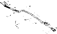
- 238000001493 electron microscopy Methods 0.000 description 1
- 238000001704 evaporation Methods 0.000 description 1
- 239000000835 fiber Substances 0.000 description 1
- 239000011521 glass Substances 0.000 description 1
- 238000009413 insulation Methods 0.000 description 1
- 239000011229 interlayer Substances 0.000 description 1
- 238000000608 laser ablation Methods 0.000 description 1
- 239000006194 liquid suspension Substances 0.000 description 1
- 238000011068 loading method Methods 0.000 description 1
- 230000007935 neutral effect Effects 0.000 description 1
- 238000010422 painting Methods 0.000 description 1
- JTJMJGYZQZDUJJ-UHFFFAOYSA-N phencyclidine Chemical compound C1CCCCN1C1(C=2C=CC=CC=2)CCCCC1 JTJMJGYZQZDUJJ-UHFFFAOYSA-N 0.000 description 1
- 238000001020 plasma etching Methods 0.000 description 1
- 239000004033 plastic Substances 0.000 description 1
- 229920003023 plastic Polymers 0.000 description 1
- 229920000642 polymer Polymers 0.000 description 1
- 239000002897 polymer film coating Substances 0.000 description 1
- 238000004080 punching Methods 0.000 description 1
- 238000007650 screen-printing Methods 0.000 description 1
- 239000002689 soil Substances 0.000 description 1
- 239000007787 solid Substances 0.000 description 1
- 238000004381 surface treatment Methods 0.000 description 1
- 238000012360 testing method Methods 0.000 description 1
Images

Classifications
-
- G—PHYSICS
- G11—INFORMATION STORAGE
- G11B—INFORMATION STORAGE BASED ON RELATIVE MOVEMENT BETWEEN RECORD CARRIER AND TRANSDUCER
- G11B5/00—Recording by magnetisation or demagnetisation of a record carrier; Reproducing by magnetic means; Record carriers therefor
- G11B5/40—Protective measures on heads, e.g. against excessive temperature
-
- G—PHYSICS
- G11—INFORMATION STORAGE
- G11B—INFORMATION STORAGE BASED ON RELATIVE MOVEMENT BETWEEN RECORD CARRIER AND TRANSDUCER
- G11B5/00—Recording by magnetisation or demagnetisation of a record carrier; Reproducing by magnetic means; Record carriers therefor
- G11B5/48—Disposition or mounting of heads or head supports relative to record carriers ; arrangements of heads, e.g. for scanning the record carrier to increase the relative speed
- G11B5/4806—Disposition or mounting of heads or head supports relative to record carriers ; arrangements of heads, e.g. for scanning the record carrier to increase the relative speed specially adapted for disk drive assemblies, e.g. assembly prior to operation, hard or flexible disk drives
- G11B5/484—Integrated arm assemblies, e.g. formed by material deposition or by etching from single piece of metal or by lamination of materials forming a single arm/suspension/head unit
-
- H—ELECTRICITY
- H05—ELECTRIC TECHNIQUES NOT OTHERWISE PROVIDED FOR
- H05K—PRINTED CIRCUITS; CASINGS OR CONSTRUCTIONAL DETAILS OF ELECTRIC APPARATUS; MANUFACTURE OF ASSEMBLAGES OF ELECTRICAL COMPONENTS
- H05K1/00—Printed circuits
- H05K1/02—Details
- H05K1/0213—Electrical arrangements not otherwise provided for
- H05K1/0254—High voltage adaptations; Electrical insulation details; Overvoltage or electrostatic discharge protection ; Arrangements for regulating voltages or for using plural voltages
- H05K1/0257—Overvoltage protection
- H05K1/0259—Electrostatic discharge [ESD] protection
-
- H—ELECTRICITY
- H05—ELECTRIC TECHNIQUES NOT OTHERWISE PROVIDED FOR
- H05K—PRINTED CIRCUITS; CASINGS OR CONSTRUCTIONAL DETAILS OF ELECTRIC APPARATUS; MANUFACTURE OF ASSEMBLAGES OF ELECTRICAL COMPONENTS
- H05K3/00—Apparatus or processes for manufacturing printed circuits
- H05K3/0091—Apparatus for coating printed circuits using liquid non-metallic coating compositions
-
- H—ELECTRICITY
- H05—ELECTRIC TECHNIQUES NOT OTHERWISE PROVIDED FOR
- H05K—PRINTED CIRCUITS; CASINGS OR CONSTRUCTIONAL DETAILS OF ELECTRIC APPARATUS; MANUFACTURE OF ASSEMBLAGES OF ELECTRICAL COMPONENTS
- H05K9/00—Screening of apparatus or components against electric or magnetic fields
- H05K9/0067—Devices for protecting against damage from electrostatic discharge
-
- H—ELECTRICITY
- H05—ELECTRIC TECHNIQUES NOT OTHERWISE PROVIDED FOR
- H05K—PRINTED CIRCUITS; CASINGS OR CONSTRUCTIONAL DETAILS OF ELECTRIC APPARATUS; MANUFACTURE OF ASSEMBLAGES OF ELECTRICAL COMPONENTS
- H05K1/00—Printed circuits
- H05K1/02—Details
- H05K1/03—Use of materials for the substrate
- H05K1/0393—Flexible materials
-
- H—ELECTRICITY
- H05—ELECTRIC TECHNIQUES NOT OTHERWISE PROVIDED FOR
- H05K—PRINTED CIRCUITS; CASINGS OR CONSTRUCTIONAL DETAILS OF ELECTRIC APPARATUS; MANUFACTURE OF ASSEMBLAGES OF ELECTRICAL COMPONENTS
- H05K1/00—Printed circuits
- H05K1/16—Printed circuits incorporating printed electric components, e.g. printed resistor, capacitor, inductor
- H05K1/167—Printed circuits incorporating printed electric components, e.g. printed resistor, capacitor, inductor incorporating printed resistors
-
- H—ELECTRICITY
- H05—ELECTRIC TECHNIQUES NOT OTHERWISE PROVIDED FOR
- H05K—PRINTED CIRCUITS; CASINGS OR CONSTRUCTIONAL DETAILS OF ELECTRIC APPARATUS; MANUFACTURE OF ASSEMBLAGES OF ELECTRICAL COMPONENTS
- H05K2201/00—Indexing scheme relating to printed circuits covered by H05K1/00
- H05K2201/03—Conductive materials
- H05K2201/032—Materials
- H05K2201/0323—Carbon
-
- H—ELECTRICITY
- H05—ELECTRIC TECHNIQUES NOT OTHERWISE PROVIDED FOR
- H05K—PRINTED CIRCUITS; CASINGS OR CONSTRUCTIONAL DETAILS OF ELECTRIC APPARATUS; MANUFACTURE OF ASSEMBLAGES OF ELECTRICAL COMPONENTS
- H05K2201/00—Indexing scheme relating to printed circuits covered by H05K1/00
- H05K2201/03—Conductive materials
- H05K2201/032—Materials
- H05K2201/0329—Intrinsically conductive polymer [ICP]; Semiconductive polymer
-
- H—ELECTRICITY
- H05—ELECTRIC TECHNIQUES NOT OTHERWISE PROVIDED FOR
- H05K—PRINTED CIRCUITS; CASINGS OR CONSTRUCTIONAL DETAILS OF ELECTRIC APPARATUS; MANUFACTURE OF ASSEMBLAGES OF ELECTRICAL COMPONENTS
- H05K2203/00—Indexing scheme relating to apparatus or processes for manufacturing printed circuits covered by H05K3/00
- H05K2203/05—Patterning and lithography; Masks; Details of resist
- H05K2203/0502—Patterning and lithography
- H05K2203/0534—Offset printing, i.e. transfer of a pattern from a carrier onto the substrate by using an intermediate member
-
- H—ELECTRICITY
- H05—ELECTRIC TECHNIQUES NOT OTHERWISE PROVIDED FOR
- H05K—PRINTED CIRCUITS; CASINGS OR CONSTRUCTIONAL DETAILS OF ELECTRIC APPARATUS; MANUFACTURE OF ASSEMBLAGES OF ELECTRICAL COMPONENTS
- H05K2203/00—Indexing scheme relating to apparatus or processes for manufacturing printed circuits covered by H05K3/00
- H05K2203/09—Treatments involving charged particles
- H05K2203/095—Plasma, e.g. for treating a substrate to improve adhesion with a conductor or for cleaning holes
-
- H—ELECTRICITY
- H05—ELECTRIC TECHNIQUES NOT OTHERWISE PROVIDED FOR
- H05K—PRINTED CIRCUITS; CASINGS OR CONSTRUCTIONAL DETAILS OF ELECTRIC APPARATUS; MANUFACTURE OF ASSEMBLAGES OF ELECTRICAL COMPONENTS
- H05K2203/00—Indexing scheme relating to apparatus or processes for manufacturing printed circuits covered by H05K3/00
- H05K2203/15—Position of the PCB during processing
- H05K2203/1545—Continuous processing, i.e. involving rolls moving a band-like or solid carrier along a continuous production path
-
- H—ELECTRICITY
- H05—ELECTRIC TECHNIQUES NOT OTHERWISE PROVIDED FOR
- H05K—PRINTED CIRCUITS; CASINGS OR CONSTRUCTIONAL DETAILS OF ELECTRIC APPARATUS; MANUFACTURE OF ASSEMBLAGES OF ELECTRICAL COMPONENTS
- H05K3/00—Apparatus or processes for manufacturing printed circuits
- H05K3/10—Apparatus or processes for manufacturing printed circuits in which conductive material is applied to the insulating support in such a manner as to form the desired conductive pattern
- H05K3/12—Apparatus or processes for manufacturing printed circuits in which conductive material is applied to the insulating support in such a manner as to form the desired conductive pattern using thick film techniques, e.g. printing techniques to apply the conductive material or similar techniques for applying conductive paste or ink patterns
- H05K3/1275—Apparatus or processes for manufacturing printed circuits in which conductive material is applied to the insulating support in such a manner as to form the desired conductive pattern using thick film techniques, e.g. printing techniques to apply the conductive material or similar techniques for applying conductive paste or ink patterns by other printing techniques, e.g. letterpress printing, intaglio printing, lithographic printing, offset printing
-
- H—ELECTRICITY
- H05—ELECTRIC TECHNIQUES NOT OTHERWISE PROVIDED FOR
- H05K—PRINTED CIRCUITS; CASINGS OR CONSTRUCTIONAL DETAILS OF ELECTRIC APPARATUS; MANUFACTURE OF ASSEMBLAGES OF ELECTRICAL COMPONENTS
- H05K3/00—Apparatus or processes for manufacturing printed circuits
- H05K3/22—Secondary treatment of printed circuits
- H05K3/28—Applying non-metallic protective coatings
Landscapes
- Engineering & Computer Science (AREA)
- Microelectronics & Electronic Packaging (AREA)
- Manufacturing & Machinery (AREA)
- Non-Metallic Protective Coatings For Printed Circuits (AREA)
- Manufacturing Of Printed Wiring (AREA)
- Structure Of Printed Boards (AREA)
- Application Of Or Painting With Fluid Materials (AREA)
- Laminated Bodies (AREA)
Abstract
A flexible circuit (10) incorporating an electrostatic discharge limiting feature, comprising a dielectric substrate selected from polyimide or liquid crystal polymer film having at least one conductive trace (30) coated on at least one surface of the substrate wherein the discharge limiting feature includes a thin conductive polymer coating (60) selectively applied over a at least a portion of the non-critical region (50) of the circuit, said feature reducing the surface resistivity of the circuit to about 10<4>ohms to about 10<8> ohms and having tribocharging of less than about 50 V.
Description
Background of invention
Little flexible circuit is widely used in the electrical connection based on flexible circuit such as integrated circuit (IC), card, Inkjet Cartridge, hard disk drive (HDD), medical apparatus and other advanced person.This class is connected to be made and assembling comprises in the product of insulating material (plastics, condensate) and the manually-operated process and needs the Electrostatic Discharge protection.The problem that ESD was concerned about is more to highlight at the hard disk manufacturing environment with in using, particularly for using big mangneto to read the head gimbal assembly of (GMR) transducer in sliding contact.Present commercial hard disk drive (HDD) production platform is at 40 to 60 megabit/inches
2[(GB)/in
2], need electrostatic discharge (ESD) protection to protect these responsive reading magnetic heads.The requirement of ESD can be according to specifying at all input blocks with near surface resistivity and triboelectric charge (tribocharge) voltage that processing/fitter's bench is controlled.Many HDD manufacturer technical specifications show that the index of surface resistivity should preferably be controlled at from about 10
4Ohm is to about 10
8In the scope of ohm, and the maximum surface voltage that has triboelectric charge to produce must be less than 10 volts (V).
Development course figure according to up-to-date HGA technology, the planning of HDD will be at 80 to 100GB/ dishes or higher in future, and also will have strict more ESD requirement (triboelectric charge is less than 5V) to the input block that comprises the flexible circuit that is applicable to suspend crooked (FOS).Microdrive program, complicated sliding contact structure and other are based on being electrically connected of suspending and adhere to the ESD that also all needs good control.By the loss that the damage that ESD caused has accounted for the most of HGA output in the HDD industry, this affects the interests of whole industry significantly.Therefore, for the HDD industry, the ability of control ESD is crucial.
In United States Patent (USP) (sequence number No.09/823,220), this application conductive compositions that will approach, narrow strip is coated between the conducting element of two flexible circuits at least, with the accumulation that reduces electrostatic charge and be equilibrated at electromotive force between all conductive lead wires.This application has also disclosed conductive polymer layers set under the protection cover layer can be so that final FOS circuit can be by the strict ionic soil test of HDD industry.
Yet, have been found that now the flexible circuit with conductive polymer coating that coating approaches on the flexible circuit part of non-critical region can reduce the surface voltage that records fully.
Summary of the invention
The present invention is a kind of flexible circuit, and this circuit is in conjunction with electrostatic charge (ESD) limited characteristic and be designed for the manufacturing of the applied hard disk drive of computer.
According to one embodiment of present invention, but in order to reduce surface measurements voltage, thin conductive polymer coating can be coated in the partially flexible circuit in the non-critical region, can flow by the electric charge that on institute's coating surface, causes, make that can discharge quickly in affected zone when the probe of conductive earthing contacts by triboelectric charge.Conductive layer is because its intrinsic resistivity has limited the speed of discharging.If coating is contacted with the conductive polymer band, then the electric charge that is produced also can be by the probe discharge that contacts with coated non-critical surface.Final circuit has the esd protection that is added; because by electric charge in case set up just to begin immediately to discharge and make conductive surface to discharge to formed any electric charge in its surface; therefore, reduce the crest voltage on surface by the decay that allows to and control voltage level.Because when energy is that the existing energy of the time damage GMR magnetic head by sensitive G MR sensors coupled is directly proportional with voltage level, so total energy will reduce.
Thin conductive film will obviously reduce the surface resistivity of insulating material, can be from about 10
11Ohm is to 10
14The scope of ohm is decreased to about 10
4Ohm is to 10
8The scope of ohm.
Just as used herein, these terms can have following connotation:
(1) term " non-critical region " is meant in the driver flexible bonding zone of circuit and the zone of the circuit between the universal joint zone.This is usually to be used to the part of handing in assembling process.
(2) term " interlayer materials " and " intermediate layer " are meant layer of material, for example, are arranged on the lax gasket material below the circuit, can be used for by and close the flexible circuit band transferred to printing mechanism.
Brief description of drawings
Fig. 1 is the profile of employed flexible circuit in hard disk drive, and it has the feature of the conductive polymer film layer in the circuit non-critical region arranged according to the present invention.
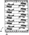
Fig. 2 is a schematic diagram of realizing the inventive method.
Fig. 3 has shown that an example has been coated in the example of the printed pattern between the flexible circuit band.
Fig. 4 shown circuit surface resistivity and in the conductive polymer composition relation between the NMP percentage.
Fig. 5 has shown in the relation of using before circuit surface resistivity and the coated with conductive condensate composition between the plasma treatment step.
Specific implementation method
The present invention is a kind of flexible circuit 10, and it combines the Electrostatic Discharge limited characteristic, as shown in Figure 1, and is designed in the manufacturing of hard disk drive.Be typically, HGA adopts hand assembled.In this operating process, when the probe that adopts non-ground connection, instrument or anchor clamps contact the coating of insulation, protection, when perhaps contacting other dielectric material such as rubber blanket, will produce electrostatic charge on the surface of flexible circuit.According to one embodiment of present invention, Bao conductive polymer coating 60 is coated on the partially flexible circuit 10 in the non-critical region 50.Non-critical region is at the driver flexible bonding zone 20 of circuit 70 and the circuit region between the universal joint zone.This is usually to be used to the part of handing in assembling process.The conductive polymer coating can be coated in selective deposition protective finish 40 above.Can obviously reduce the surface resistivity of material by the formed conductive membrane layer of conductive polymer coating, can be from about 10
11Ohm is to 10
14The scope of ohm is decreased to about 10
4Ohm is to 10
8The scope of ohm.In the present embodiment, in order to avoid ESD in the protective circuit surface, the coating of conductive polymer not necessarily will contact the lead-in wire of conduction.
The conductive polymer composition can adopt a cylinder to the typography of cylinder to apply continuously, to form thin conductive polymer film element, its final cured thickness about 0.2 micron to about 25 microns scope, preferably about 0.5 micron to about 5 microns scope, it can be coated on the various insulating material, for example, polymer thin films, frosting, pottery, glass, fiber, and particularly be coated on the flexible circuit.Flexible circuit can be that polyimides also can be the dielectric substrate of liquid crystal polymer, has a conducting wire at least one surface of dielectric substrate at least.This conducting wire can be by at least one surface that photoresist is coated in dielectric substrate, adopt the circuitry needed figure that photoresist is carried out graphically, and adopt such as copper, nickel, golden the described circuitous pattern of metal pair carry out that the method for additional plated forms.In addition, the method that also can adopt subtraction to form circuit is created flexible circuit.Can adopt the characteristic such as chemical etching, laser ablation, mechanical punching and other or the like method forms compressing of perforation, blind hole, window, dielectric substrate or thinner zone and other or the like in dielectric film.After forming circuit, protectiveness condensate composition can optionally apply also can globality be coated on the circuit.The conductive polymer composition can be coated on this protective coating surface subsequently.
The present invention be more particularly directed to a kind of flexible circuit of the HGA of being applicable to parts, the surface resistivity of these HGA parts is about 10
4Ohm is to 10
8In the scope of ohm, and according to the surface resistivity of conductive polymer film coating, triboelectric charge is less than 50V, more preferably less than 15V.
Example
Preferable conductive polymer composition comprises the mixture of conductive polymer, nonionic binding material, wetting agent and film former.
A kind of preferable conductive polymer is a kind ofly to have that (Bayer Corporation ofPittsburgh PA) produces, trade mark is Baytron by Beyer Co., Ltd
TMThe water-based diffusant of the poly--3-4-dioxy ethene thiophene (Poly-3-4-ethylenedioxythiophene) of the mixing poly styrene sulfonate of P-LS (polystyrene sulfonate), it has low survivor ion capacity.The conducting polymer liquid suspension that is provided has and is approximately 1% to 4% solids by weight.
A kind of preferable nonionic binding material is Rhoplex HA-16, and this is a kind of by Rohm and Haas company (Rohm and Haas Company of Philadelphia, PA) the self-crosslinking acrylic binding agent of Chu Pining.
A kind of preferable wetting agent is by Dupont chemical company (Dupont Chemical Company, Wilmington, DE) Zonyl of Chu Pining
FSN.Its chemical constitution is " R
fCH
2CH
2O (CH
2CH
2O)
xH ", R in the formula
f=F (CF
2CF
2)
y, wherein, X=0 is to about 25, and Y=1 is to about 9.Wetting agent can be used for changing surface energy with low-down concentration, and is compatible with the solution of great majority based on water-based or solvent.Generally, the lubricant concentration of adding about 0.1% to about 0.5% scope, by weight.
Preferable additive is 1-methyl-2-pyrolidone (NMP).The function of NMP is to be convenient to discharge from the main framework of conductive polymer chain more " free ion ", to increase conductivity.The degree that conductivity is improved depends primarily on the quantity of the NMP that is added.The NMP that is added is about 2% to about 8% scope, by weight, and more preferably about 2% to about 4% scope, by weight.
The conductive polymer composition can be made by the combination of mentioned component.Particularly, 10% to the 90% conductive polymer diffusant (Baytron P-LS) that provides has been sneaked into selected lubricant in this diffusant.This diffusant can 90% to 10% acrylic emulsion (RHOPLEX HA-16) and 2% to 8%NMP mixture make up.Subsequently, the ph value of final mixture can be by 50% ammonium hydroxide (NH of interpolation about 0.1% to 1%
4OH) solution is adjusted in about 7.0 and 8.5 the scope from about 3.0.Table 1 has shown the example of a group profile.
Table 1
Be applicable to the exemplary formula of conductive polymer composition and final conductive polymer film performance
| Example 1.1 | Example 1.2 | Example 1.3 | Example 1.4 | Example 1.5 | |
| ??BAYTRON?P-LS | ??90wt.% | ??88.2wt.% | ??86.4wt.% | ??82.8wt.% | ??72wt.% |
| ??RHOPLEX?HA-16 | ??10wt.% | ??9.8wt.% | ??9.6wt.% | ??9.2wt.% | ??8wt.% |
| ??NMP | ??0 | ??2wt.% | ??4wt.% | ??8wt.% | ??20wt.% |
| Triboelectric charge | ??10-50V | ??10-30V | ??5-15V | ??<10V | ??<10V |
Attention: all conductive polymer compositions all comprise the Zonyl of 0.1%-0.3%
FSN.
The conductive polymer composition can adopt a cylinder to be coated in the non-critical region of FOS circuit to the place mat print system of cylinder, the place mat print system comprises that one can be handled from about 70mm to approximately 300mm is wide, the preferably automatic strip treatment system of the wide band of 70mm, a print station and a drying table.The structure of this system and assembling are as shown in Figure 2.Before or after protective coating applies, can give integrated with the manufacturing of FOS circuit or this technology is being used as independent technology aspect the final band of the flexible circuit with protective finish by shifting out tape handling equipment and print station being inserted in the flexible circuitry production line this treatment process.
In place mat printing treatment technology, paper liner or condensate liner can be placed on little flexible band below, can have the ink of preventing like this and flow to and be diffused into unwanted zone.The placement tolerance of following band can be by sprocket wheel perforation (shown in Figure 3 320) control, and this hole is arranged on the side of flexible circuit band 300, and can be in band down with 32 spacing cumulative errors for+/-mode of 0.254mm represents.The tolerance of the band printing of intersecting depends on the circuit of coating sometimes, but is typically about 40 Mills.
Automatically the tape handling system can handle from about 70mm to the wide band of about 300mm, preferably, the band that 70mm is wide, the band that it is included in before the print station 220 is decontroled platform 205, and the band rolling platform 260 after baking oven 245.Loosen platform and can hold the material of two cylinders down, that is, and the intermediate layer material 210 of the band of flexible circuit 215 and a cylinder.The purpose of intermediate layer material is to help to comprise before solvent evaporation the conductive polymer composition.The width in the intermediate layer width with the flexible circuit band basically is identical.Be fitted on the circuit surface that transmitted by control and become dosis refracta with conductive polymer on the zone, the adjection that the back side that allows circuit also can apply can be played in the intermediate layer, thereby circuit is provided the protection of other ESD.Usually, flexible circuit comes perforate by dielectric substrate, so that separate various piece.Quantity by control conductive polymer composition can go up coated materials overleaf by these perforates between flexible circuit dielectric substrate and intermediate layer material and pore.Intermediate layer material can be selected from one group of material that comprises convex intermediate layer, release liners or Teflon intermediate layer.The intermediate layer is to be decontroled by cylinder 210.Subsequently, by the flexible circuit cylinder, this band feeds out these cylinders with direction v with identical speed.Several idle pulleys are used to keep the elasticity of the suitable band of film.Subsequently, the flexible circuit on the intermediate layer is brought into print station 220.
The conductive polymer composition is coated in the non-critical region of the HDD circuit on the flexible circuit band.Painting method can make the trans-printing technology such as silk screen printing or liner printing.For instance, print station as shown in Figure 2 is exactly a liner print station.When flex circuit material 215 was introduced into print station, print head 230 was loading the conductive polymer composition and is being stamped in being with of passing through thereupon.Print head 230 is designed to the conductive polymer composition can be deposited on the non-critical region of HDD circuit and across the whole width (see figure 3) of band.The spacing that this step can be stipulated repeats, and each provisional capital of feasible HDD circuit on the strip length lengthwise position can adopt similar mode to impress.One cylinder absorption paper can use in conjunction with print station, as shown in Figure 2, and the required degree so that the conductive polymer composition that was comprised before solvent evaporation can keep clean.
After printing, flex circuit material enters at least one baking oven.Unnecessary solvent can be dried, and binding resin is crosslinked in baking oven.Preferable oven structure allows to carry out the step that bakes of the prebaking step of evaporating solvent and crosslinked resin and any remaining solvent of removal.The prebaking zone of baking oven can be arranged on about 40 ℃ to about 90 ℃ temperature range.After platform, that can carry out online or off-line in second baking oven bakes step at last, not shown on the circuit of prebaking is rich.Last baking temperature can be arranged on about 120 ℃ to about 180 ℃ of scopes.Baking oven can be an IR bake, also can be the high wind convection oven.
As liner printing treatment technology, it is important that conductive polymer film is in coating surface or the uniformity on exposed polyimide base film.These surfaces generally all have lower surface energy, and its scope is at the extremely about 39dyne/cm of about 28dyne/cm.Surface energy can use the marking pen of the standard surface tension solvent that comprises Sherman Treaters (UK) company product to determine.
Use Electron Microscopy, the thickness distribution scope that can determine conductive polymer film is about 0.2 micron to about 5 microns.Can adopt the mode that increases the surface energy on coating or the polyimides to detect the process for treating surface step of various routines, this should improve the uniformity of bonding and film equally.Surprisingly, the measurement of skin resistance shows, compares at least 10 times of the conductivity of plasma etching raising film with the surface that does not have using plasma to handle.Corona treatment should produce similar or better effect.
Carrying out plasma treatment before the coated with conductive condensate prescription on the circuit.The gaseous plasma of mixing be can use, argon gas, nitrogen and oxygen comprised.When about 120 ℃ of temperature, the speed of band can be set to about 3mpm.
The thickness of coating can change, by single, twice or even more times print the thickness that increases film, and its conductivity.
Skin resistance is measured can be on the single circuit surface or have from the teeth outwards on other film surface of conductive polymer film and carry out.This measurement can be used the Hiresta UP MCP-HT260 resistance instrument with HRS ring-type probe, and (Mitsubishi Chemical, Tokyo Japan) carries out.
But the ESD sensitiveness of HGA is relevant with the discharge energy of this part, and this can instruct by the GMR element of W head.If the dielectric surface of flexible circuit is with other medium or do not have the electric conducting material of ground connection to contact, when different materials separates, will set up the instantaneous voltage electromotive force, because exist unnecessary positive charge or negative electrical charge from the surface.If the surface has high resistivity, this electric charge will keep, and can not discharge or drainage.If material conducts electricity, then electric charge will spread and form neutral charge (decay).For circuit, need good dielectric material usually, make the triboelectric charge effect become very general.
Voltage level is directly relevant with the quantity of electric charge point/unit area on the circuit surface.A kind of direct surface measurements voltage method is to use Isoprobe
Electrostatic voltmeter-Model 244A (MonroeElectronics, Lyndonville, New York).For high impedance surface, can measure crest voltage or the voltage range of this part, to determine whether surface treatment has reduced measured voltage level.
Fig. 4 is presented at the surface resistivity of circuit and the relation between the NMP percentage in the conductive polymer composition, and wherein the conductive polymer composition comes from conductive polymer film for given thickness at the example shown in the table 1.This conductivity can further increase by applying thicker film.
Fig. 5 is presented at the surface resistivity of circuit and in the relation of using before the coated with conductive condensate composition between the plasma treatment step.The sheet resistance of pre-process circuit with do not carry out pretreated circuit and do not have the circuit of the conductive membrane layer of esd protection to compare.
Claims (16)
1. flexible circuit in conjunction with the discharge electrostatic charges limited characteristic, it is characterized in that, described circuit comprises a dielectric substrate that is selected from polyimides group or polymerizable mesogenic body thin film, has the conducting wire of at least one plating at least one surface of dielectric substrate; Described discharge limited characteristic comprises that a selectivity is coated in the thin conductive polymer coating on the part non-critical region of described at least circuit, and described characteristic is decreased to the surface resistivity of circuit about 10
4Ohm is to 10
8Ohm, and the triboelectric charge that is had is less than about 50V.
2. according to the described flexible circuit of claim 1, it is characterized in that, described conductive polymer coating comprises the water-based diffusant of about 10 to 90 percentage by weights of at least 1.3 percentage by weight conductive polymers, about 10 aqueous emulsions of the nonionic self-crosslinking acrylic binding resin of about 4.5 percentage by weights to about 90 percentage by weights,, and the aqueous solvent of 0.1 to 1 percentage by weight of the ammonium hydroxide of about 50 percentage by weights.
3. according to the described flexible circuit of claim 2, it is characterized in that, the mixture of described discharge limited characteristic comprises poly--3-4-dioxy ethene thiophene (Poly-3-4-ethylenedioxythiophene) and poly styrene sulfonate (polystyrene sulfonate), wherein the water-based diffusant contains from about 2% to about 3% conductive polymer.
4. according to the described flexible circuit of claim 1, it is characterized in that described conductive polymer is to the visible spectrum substantially transparent.
5. according to the described flexible circuit of claim 1, it is characterized in that, further be included in the protective finish of the selective deposition on the described circuit-line, described conductive polymer coating is to apply in the above.
6. according to the described flexible circuit of claim 1, it is characterized in that, described circuit-line is by at least one surface that photoresist is coated in described dielectric substrate, adopt described circuitous pattern that photoresist is carried out graphically, and adopt to be selected from and comprise copper, nickel and gold and so on conducting metal the method that described circuitous pattern carries out additional plated is formed.
7. according to the described flexible circuit of claim 1, it is characterized in that, comprise that further at least one characteristic is selected from the group that is included in formed perforation, blind hole, window and breach in the described dielectric substrate.
8. according to the described flexible circuit of claim 1, it is characterized in that described triboelectric charge is less than 15V.
9. according to the described flexible circuit of claim 1, it is characterized in that described triboelectric charge is less than 10V.
10. device that is applicable to formation in conjunction with the flexible circuit of static discharge limited characteristic, it is characterized in that, described this circuit comprises a dielectric substrate, described dielectric substrate has the conducting wire of a plating at least on one surface at least, and selectivity is coated in the thin conductive polymer coating on the part non-critical region of described at least circuit, described coating can adopt automatic tape handling system to form, described automatic tape handling system can handle width from about 70mm to the about wide band of 300mm, and comprise a band relieving platform before print station, a baking oven and the band rolling platform after baking oven, described band are decontroled platform and are had the cylinder that is used for a flexible circuit cylinder and an intermediate layer cylinder.
11. one kind is applicable to that selectivity forms the printing treatment technology of a continuous cylinder of thin conductive polymer coating to cylinder, described conductive polymer coating be coated in a plurality of flexible circuits to the small part non-critical region, it is characterized in that described treatment process comprises:
The intermediate layer material of one cylinder and the flexible circuit of a cylinder are provided, described flexible circuit has a plurality of with the capable circuit that is positioned on the cylinder transverse width, and the row of a plurality of longitudinal registers along cylinder, decontrol intermediate layer material to being with from cylinder, come moving belt and intermediate layer material cylinder with band direction and the speed that sets by flexible circuit, flexible circuit is fed out from cylinder with identical speed with the band direction, nationality helps the elasticity that a plurality of idle pulleys come retainer belt simultaneously, to be with the shift-in print station, nationality help the trans-printing technology with across the mode of delegation's flexible circuit with the conductive polymer composition be coated in the described flexible circuit to the small part non-critical region, with the spacing of band direction with a regulation of Tape movement, the step of on the adjacent lines of flexible circuit, repeating print, print steps repeats prescribed distance, thereby print each row, and will be with the shift-in drying oven.
12. according to the described processing of claim 11, it is characterized in that, further be included in print steps plasma treatment step before.
13., it is characterized in that use a kind of mixed gas plasma, mist comprises argon gas, nitrogen and oxygen according to the described processing of claim 12.
14. according to the described processing of claim 11, it is characterized in that, further be included in print steps corona treatment before.
15. according to the described processing of claim 11, it is characterized in that, described each circuit carried out repeatedly coating step.
16. according to the described processing of claim 11, it is characterized in that, unnecessary conductive polymer composition is coated on the circuit band, so that redundance flows through perforate in band and the pore between intermediate layer material and circuit band also apply described dielectric substrate with the thin layer conductive polymer the back side.
Applications Claiming Priority (2)
| Application Number | Priority Date | Filing Date | Title |
|---|---|---|---|
| US10/255,507 | 2002-09-26 | ||
| US10/255,507 US6815620B2 (en) | 2001-03-29 | 2002-09-26 | Flexible circuit with electrostatic damage limiting feature |
Publications (1)
| Publication Number | Publication Date |
|---|---|
| CN1685774A true CN1685774A (en) | 2005-10-19 |
Family
ID=32041750
Family Applications (1)
| Application Number | Title | Priority Date | Filing Date |
|---|---|---|---|
| CNA038227762A Pending CN1685774A (en) | 2002-09-26 | 2003-08-29 | Flexible circuit with electrostatic damage limiting feature |
Country Status (5)
| Country | Link |
|---|---|
| US (2) | US6815620B2 (en) |
| JP (1) | JP2006500782A (en) |
| CN (1) | CN1685774A (en) |
| AU (1) | AU2003263041A1 (en) |
| WO (1) | WO2004030427A1 (en) |
Cited By (3)
| Publication number | Priority date | Publication date | Assignee | Title |
|---|---|---|---|---|
| CN101202212B (en) * | 2006-12-11 | 2011-03-23 | 爱德牌工程有限公司 | Substrate damage prevention system and method |
| CN104078055A (en) * | 2013-03-29 | 2014-10-01 | 东莞新科技术研究开发有限公司 | Flexible piece, manufacturing method thereof, head-gimbal assembly and disc drive |
| CN113271719A (en) * | 2021-06-23 | 2021-08-17 | 昆山丘钛生物识别科技有限公司 | Flexible circuit board processing method, device and equipment |
Families Citing this family (13)
| Publication number | Priority date | Publication date | Assignee | Title |
|---|---|---|---|---|
| US6995954B1 (en) | 2001-07-13 | 2006-02-07 | Magnecomp Corporation | ESD protected suspension interconnect |
| US7489493B2 (en) * | 2003-12-01 | 2009-02-10 | Magnecomp Corporation | Method to form electrostatic discharge protection on flexible circuits using a diamond-like carbon material |
| US7223922B2 (en) * | 2004-07-28 | 2007-05-29 | International Business Machines Corporation | ESD dissipative coating on cables |
| US7525047B2 (en) * | 2004-07-28 | 2009-04-28 | International Business Machines Corporation | Cable having translucent, semi-transparent or transparent ESD dissipative layer and/or metallic layer |
| JP4386863B2 (en) * | 2005-02-21 | 2009-12-16 | 日本発條株式会社 | Head suspension |
| JP4326484B2 (en) * | 2005-02-21 | 2009-09-09 | 日本発條株式会社 | Head suspension |
| JP4571013B2 (en) * | 2005-05-30 | 2010-10-27 | 日東電工株式会社 | Printed circuit board |
| US8213120B2 (en) * | 2007-09-10 | 2012-07-03 | International Business Machines Corporation | Flexible cable comprising liquid crystal polymer |
| JP5138549B2 (en) | 2008-10-31 | 2013-02-06 | 日東電工株式会社 | Suspension board with circuit |
| US8493689B2 (en) * | 2009-06-15 | 2013-07-23 | Seagate Technology Llc | Protective layer on gimbal for scratch mitigation |
| US8873192B1 (en) | 2013-07-30 | 2014-10-28 | Hewlett-Packard Development Company, L.P. | Magnetic tape heads |
| US9681542B2 (en) * | 2014-11-14 | 2017-06-13 | Oracle International Corporation | Flexible circuit with partial ground path |
| CN107710889B (en) * | 2015-05-06 | 2021-06-29 | 哈钦森技术股份有限公司 | Plasma treatment of flexures for hard disk drives |
Family Cites Families (43)
| Publication number | Priority date | Publication date | Assignee | Title |
|---|---|---|---|---|
| US3562037A (en) * | 1967-07-07 | 1971-02-09 | Electro Connective Systems Inc | Continuous method of producing indefinite lengths of flexible flat electrical conductors |
| US4231154A (en) * | 1979-01-10 | 1980-11-04 | International Business Machines Corporation | Electronic package assembly method |
| EP0030792B1 (en) * | 1979-11-20 | 1983-09-21 | National Research Development Corporation | Infra red reflectors |
| EP0049032B1 (en) * | 1980-08-21 | 1986-09-17 | National Research Development Corporation | Coating insulating materials by glow discharge |
| DE3200206A1 (en) * | 1982-01-07 | 1983-07-21 | Henkel KGaA, 4000 Düsseldorf | ORGANOPOLYSILOXANES AND THEIR USE AS ANTI-FOAM AGENTS IN AQUEOUS DISPERSIONS AND SOLUTIONS OF RESIN |
| US4576964A (en) * | 1982-03-16 | 1986-03-18 | Pfizer Inc. | Substituted hexahydrobenzo[e]indene and octahydrophenanthrene CNS agents and pharmaceutical compositions thereof |
| US4480288A (en) * | 1982-12-27 | 1984-10-30 | International Business Machines Corporation | Multi-layer flexible film module |
| US4698256A (en) * | 1984-04-02 | 1987-10-06 | American Cyanamid Company | Articles coated with adherent diamondlike carbon films |
| FR2592874B1 (en) * | 1986-01-14 | 1990-08-03 | Centre Nat Rech Scient | PROCESS FOR DIPPING A GLASS OR VITREOUS OBJECT AND OBJECT THUS DIPPED |
| US4809876A (en) * | 1987-08-27 | 1989-03-07 | Aluminum Company Of America | Container body having improved gas barrier properties |
| US4913930A (en) * | 1988-06-28 | 1990-04-03 | Wacker Silicones Corporation | Method for coating semiconductor components on a dielectric film |
| US4914551A (en) * | 1988-07-13 | 1990-04-03 | International Business Machines Corporation | Electronic package with heat spreader member |
| US4959752A (en) * | 1988-10-24 | 1990-09-25 | Digital Equipment Corporation | Electronic module RFI/EMI shielding |
| CA2031098A1 (en) * | 1990-01-16 | 1991-07-17 | William F. Banholzer | Cvd diamond coated annulus components and method of their fabrication |
| US5527596A (en) * | 1990-09-27 | 1996-06-18 | Diamonex, Incorporated | Abrasion wear resistant coated substrate product |
| WO1993014504A1 (en) * | 1992-01-18 | 1993-07-22 | The University Of Newcastle Upon Tyne | Process for the preparation of conductive polymers |
| US5227008A (en) * | 1992-01-23 | 1993-07-13 | Minnesota Mining And Manufacturing Company | Method for making flexible circuits |
| DE4219410A1 (en) * | 1992-06-13 | 1993-12-16 | Hoechst Ag | Heat-sealable, antistatic-coated films and film laminates, processes for their production and their use |
| US5350594A (en) * | 1993-01-25 | 1994-09-27 | Tech Spray, Inc. | Conformally coated faraday cage |
| EP0615257B1 (en) | 1993-03-09 | 1999-06-02 | Koninklijke Philips Electronics N.V. | Method of manufactoring a laminated structure of a metal layer on a conductive polymer layer |
| EP0698275A4 (en) * | 1993-04-28 | 1996-09-04 | Mark Mitchnick | Conductive polymers |
| US5401913A (en) * | 1993-06-08 | 1995-03-28 | Minnesota Mining And Manufacturing Company | Electrical interconnections between adjacent circuit board layers of a multi-layer circuit board |
| US5643343A (en) * | 1993-11-23 | 1997-07-01 | Selifanov; Oleg Vladimirovich | Abrasive material for precision surface treatment and a method for the manufacturing thereof |
| US5465186A (en) * | 1994-01-26 | 1995-11-07 | International Business Machines Corporation | Shorted magnetoresistive head leads for electrical overstress and electrostatic discharge protection during manufacture of a magnetic storage system |
| US5559367A (en) * | 1994-07-12 | 1996-09-24 | International Business Machines Corporation | Diamond-like carbon for use in VLSI and ULSI interconnect systems |
| US5551959A (en) * | 1994-08-24 | 1996-09-03 | Minnesota Mining And Manufacturing Company | Abrasive article having a diamond-like coating layer and method for making same |
| US5700398A (en) | 1994-12-14 | 1997-12-23 | International Business Machines Corporation | Composition containing a polymer and conductive filler and use thereof |
| JP2855414B2 (en) | 1995-04-13 | 1999-02-10 | 日本メクトロン株式会社 | Relay substrate for magnetic head and method of manufacturing the same |
| US6099757A (en) * | 1995-06-05 | 2000-08-08 | Americhem, Inc. | Tuned conductive coatings and blends from intrinisically conductive polymers and processes for making same |
| US5761009A (en) * | 1995-06-07 | 1998-06-02 | International Business Machines Corporation | Having parastic shield for electrostatic discharge protection |
| DE19536844C1 (en) * | 1995-10-02 | 1997-04-10 | Bayer Ag | Process for electrostatic painting of non-conductive surfaces |
| JP3062435B2 (en) * | 1995-11-10 | 2000-07-10 | 日本碍子株式会社 | Flexible substrate, Be-Cu alloy foil used therefor, and method of manufacturing the same |
| US5644454A (en) * | 1996-03-11 | 1997-07-01 | International Business Machines Corporation | Electrostatic discharge protection system for MR heads |
| US5699212A (en) * | 1996-05-01 | 1997-12-16 | International Business Machines Corporation | Method of electrostatic discharge protection of magnetic heads in a magnetic storage system |
| US6046886A (en) * | 1997-10-09 | 2000-04-04 | Seagate Technology, Inc. | Flex circuit head interconnect with insulating spacer |
| KR100442408B1 (en) * | 1998-11-05 | 2004-11-06 | 제일모직주식회사 | Polythiophene Conductive Polymer Solution Composition with High Conductivity and High Transparency |
| US6125015A (en) * | 1998-12-04 | 2000-09-26 | Read-Rite Corporation | Head gimbal assembly with low stiffness flex circuit and ESD Protection |
| US6146813A (en) * | 1999-01-13 | 2000-11-14 | Applied Kinetics Inc. | Method and shunting and deshunting an electrical component and a shuntable/shunted electrical component |
| US6316734B1 (en) * | 2000-03-07 | 2001-11-13 | 3M Innovative Properties Company | Flexible circuits with static discharge protection and process for manufacture |
| US6687097B1 (en) * | 2000-03-22 | 2004-02-03 | Pemstar, Inc. | Electrostatic protection for magnetic heads |
| US6482521B1 (en) | 2000-07-31 | 2002-11-19 | Hughes Electronics Corp. | Structure with blended polymer conformal coating of controlled electrical resistivity |
| US6927951B2 (en) * | 2001-03-09 | 2005-08-09 | Seagate Technology Llc | Flex on suspension with dissipative polymer substrate acting as bleed resistor for minimizing ESD damage |
| US6459043B1 (en) * | 2001-03-29 | 2002-10-01 | 3M Innovative Properties Company | Flexible circuit with electrostatic damage limiting feature and method of manufacture |
-
2002
- 2002-09-26 US US10/255,507 patent/US6815620B2/en not_active Expired - Fee Related
-
2003
- 2003-08-29 CN CNA038227762A patent/CN1685774A/en active Pending
- 2003-08-29 AU AU2003263041A patent/AU2003263041A1/en not_active Abandoned
- 2003-08-29 WO PCT/US2003/027362 patent/WO2004030427A1/en active Application Filing
- 2003-08-29 JP JP2004540039A patent/JP2006500782A/en not_active Withdrawn
-
2004
- 2004-07-22 US US10/897,139 patent/US7135203B2/en not_active Expired - Fee Related
Cited By (5)
| Publication number | Priority date | Publication date | Assignee | Title |
|---|---|---|---|---|
| CN101202212B (en) * | 2006-12-11 | 2011-03-23 | 爱德牌工程有限公司 | Substrate damage prevention system and method |
| CN104078055A (en) * | 2013-03-29 | 2014-10-01 | 东莞新科技术研究开发有限公司 | Flexible piece, manufacturing method thereof, head-gimbal assembly and disc drive |
| CN104078055B (en) * | 2013-03-29 | 2018-10-26 | 东莞新科技术研究开发有限公司 | Flexible element and its manufacturing method, magnetic head fold piece combination and disc driver |
| CN113271719A (en) * | 2021-06-23 | 2021-08-17 | 昆山丘钛生物识别科技有限公司 | Flexible circuit board processing method, device and equipment |
| CN113271719B (en) * | 2021-06-23 | 2022-07-08 | 昆山丘钛生物识别科技有限公司 | Flexible circuit board processing method, device and equipment |
Also Published As
| Publication number | Publication date |
|---|---|
| JP2006500782A (en) | 2006-01-05 |
| US6815620B2 (en) | 2004-11-09 |
| US7135203B2 (en) | 2006-11-14 |
| US20030062194A1 (en) | 2003-04-03 |
| AU2003263041A1 (en) | 2004-04-19 |
| WO2004030427A1 (en) | 2004-04-08 |
| US20040257729A1 (en) | 2004-12-23 |
Similar Documents
| Publication | Publication Date | Title |
|---|---|---|
| CN1685774A (en) | Flexible circuit with electrostatic damage limiting feature | |
| KR100377992B1 (en) | Anisotropically electroconductive resin film | |
| US6459043B1 (en) | Flexible circuit with electrostatic damage limiting feature and method of manufacture | |
| CN104519671B (en) | Carbon oil pcb board and preparation method thereof | |
| JP2001210956A (en) | Multilayer laminate | |
| US8595917B2 (en) | Method for improving a flexure's electrical characteristics | |
| KR100691336B1 (en) | Manufacturing method of flexible semiconductor substrate by buildup method | |
| EP1848253B1 (en) | Wired circuit board | |
| US20030015345A1 (en) | Laminated base sheet for flexible printed circuit board | |
| JPH06148122A (en) | Humidity detecting element | |
| JP2003208931A (en) | Connecting member | |
| US20070238361A1 (en) | Printed circuit board | |
| JP3763183B2 (en) | Humidity sensor and manufacturing method thereof | |
| CN1253465A (en) | Built-in finger-like plate capacitor resistor and manufacturing method thereof | |
| JP2000151098A (en) | Manufacture of metal base wiring board | |
| JPH06244520A (en) | Flexible printed-circuit board | |
| JPH0529739A (en) | Flexible printed circuit board | |
| JP2788576B2 (en) | Printed wiring board intermediate material | |
| CN119012506A (en) | Micro-nano circuit board and large-scale manufacturing process thereof | |
| JP2023099279A (en) | touch sensor | |
| Zhang et al. | 3M tribo-coating development and its application on microinterconnect flexible circuit | |
| TWI384910B (en) | Flexible printed circuit boards | |
| JP2003243799A (en) | Method of manufacturing flexible board | |
| Hinderaker et al. | New connector in an adhesive tape form for electronic applications | |
| JPH0529729A (en) | Flexible printed circuit board |
Legal Events
| Date | Code | Title | Description |
|---|---|---|---|
| C06 | Publication | ||
| PB01 | Publication | ||
| C10 | Entry into substantive examination | ||
| SE01 | Entry into force of request for substantive examination | ||
| C02 | Deemed withdrawal of patent application after publication (patent law 2001) | ||
| WD01 | Invention patent application deemed withdrawn after publication |