CN1663105A - Improved platen for electrostatic wafer clamping device - Google Patents
Improved platen for electrostatic wafer clamping device Download PDFInfo
- Publication number
- CN1663105A CN1663105A CN038150476A CN03815047A CN1663105A CN 1663105 A CN1663105 A CN 1663105A CN 038150476 A CN038150476 A CN 038150476A CN 03815047 A CN03815047 A CN 03815047A CN 1663105 A CN1663105 A CN 1663105A
- Authority
- CN
- China
- Prior art keywords
- platen
- thickness
- wafer
- tic
- dielectric material
- Prior art date
- Legal status (The legal status is an assumption and is not a legal conclusion. Google has not performed a legal analysis and makes no representation as to the accuracy of the status listed.)
- Granted
Links
Images


Classifications
-
- H—ELECTRICITY
- H02—GENERATION; CONVERSION OR DISTRIBUTION OF ELECTRIC POWER
- H02N—ELECTRIC MACHINES NOT OTHERWISE PROVIDED FOR
- H02N13/00—Clutches or holding devices using electrostatic attraction, e.g. using Johnson-Rahbek effect
-
- H—ELECTRICITY
- H10—SEMICONDUCTOR DEVICES; ELECTRIC SOLID-STATE DEVICES NOT OTHERWISE PROVIDED FOR
- H10P—GENERIC PROCESSES OR APPARATUS FOR THE MANUFACTURE OR TREATMENT OF DEVICES COVERED BY CLASS H10
- H10P72/00—Handling or holding of wafers, substrates or devices during manufacture or treatment thereof
- H10P72/50—Handling or holding of wafers, substrates or devices during manufacture or treatment thereof for positioning, orientation or alignment
-
- H—ELECTRICITY
- H10—SEMICONDUCTOR DEVICES; ELECTRIC SOLID-STATE DEVICES NOT OTHERWISE PROVIDED FOR
- H10P—GENERIC PROCESSES OR APPARATUS FOR THE MANUFACTURE OR TREATMENT OF DEVICES COVERED BY CLASS H10
- H10P72/00—Handling or holding of wafers, substrates or devices during manufacture or treatment thereof
- H10P72/70—Handling or holding of wafers, substrates or devices during manufacture or treatment thereof for supporting or gripping
- H10P72/72—Handling or holding of wafers, substrates or devices during manufacture or treatment thereof for supporting or gripping using electrostatic chucks
- H10P72/722—Details of electrostatic chucks
-
- Y—GENERAL TAGGING OF NEW TECHNOLOGICAL DEVELOPMENTS; GENERAL TAGGING OF CROSS-SECTIONAL TECHNOLOGIES SPANNING OVER SEVERAL SECTIONS OF THE IPC; TECHNICAL SUBJECTS COVERED BY FORMER USPC CROSS-REFERENCE ART COLLECTIONS [XRACs] AND DIGESTS
- Y10—TECHNICAL SUBJECTS COVERED BY FORMER USPC
- Y10T—TECHNICAL SUBJECTS COVERED BY FORMER US CLASSIFICATION
- Y10T279/00—Chucks or sockets
- Y10T279/23—Chucks or sockets with magnetic or electrostatic means
-
- Y—GENERAL TAGGING OF NEW TECHNOLOGICAL DEVELOPMENTS; GENERAL TAGGING OF CROSS-SECTIONAL TECHNOLOGIES SPANNING OVER SEVERAL SECTIONS OF THE IPC; TECHNICAL SUBJECTS COVERED BY FORMER USPC CROSS-REFERENCE ART COLLECTIONS [XRACs] AND DIGESTS
- Y10—TECHNICAL SUBJECTS COVERED BY FORMER USPC
- Y10T—TECHNICAL SUBJECTS COVERED BY FORMER US CLASSIFICATION
- Y10T428/00—Stock material or miscellaneous articles
- Y10T428/24—Structurally defined web or sheet [e.g., overall dimension, etc.]
- Y10T428/24802—Discontinuous or differential coating, impregnation or bond [e.g., artwork, printing, retouched photograph, etc.]
- Y10T428/24917—Discontinuous or differential coating, impregnation or bond [e.g., artwork, printing, retouched photograph, etc.] including metal layer
Landscapes
- Container, Conveyance, Adherence, Positioning, Of Wafer (AREA)
- Drying Of Semiconductors (AREA)
- Discharging, Photosensitive Material Shape In Electrophotography (AREA)
Abstract
本发明揭示了一种用于静电的晶片夹紧装置(10)中的压盘(12),其包括一介电材料的压盘体(12)和扩散在介电材料内的导电材料的颗粒,以使压盘(12)因导电颗粒的扩散而具有相当大的静电电容。这导致不管周围湿度如何,压盘(12)具有一增加了的夹紧力。根据本发明的另一方面,压盘体(12)的厚度可减小一定量,以致在从电压源(28)施加的电压降低的情形下足以保持一恒定的夹紧力,以便消除压盘上任何的残余电压并提高晶片(38)释放的速度。
The present invention discloses a platen (12) for use in an electrostatic wafer clamping device (10), comprising a platen body (12) of dielectric material and particles of conductive material dispersed within the dielectric material, such that the platen (12) has a substantial electrostatic capacitance due to the diffusion of the conductive particles. This results in the platen (12) having an increased clamping force regardless of ambient humidity. According to another aspect of the invention, the thickness of the platen body (12) can be reduced by an amount sufficient to maintain a constant clamping force under conditions where the voltage applied from the voltage source (28) is reduced, thereby eliminating any residual voltage on the platen and increasing the speed at which the wafer (38) is released.
Description
发明背景Background of the invention
本发明涉及半导体器件制造技术,具体来说,涉及一种用于半导体器件制造的新的和改进的静电晶片夹紧装置用的压盘。This invention relates to the art of semiconductor device fabrication, and more particularly, to a new and improved platen for electrostatic wafer chucking for semiconductor device fabrication.
一种在制造过程中用来夹紧半导体晶片的已知技术包括使用静电的卡盘。尽管静电卡盘在设计上有变化,但它们都根据相同的物理原理,即在压盘表面和半导体晶片之间形成一静电力。典型的静电夹具包括一导电电极,其安装在一底座上并被一电气绝缘的介电材料或压盘所覆盖。半导体晶片坐落在绝缘材料的顶上。一电压源电气地偏置电极,以使电荷积聚在电极和绝缘材料上。然后,施加的电压在晶片的后表面上包括一相等的和相对的电荷。该积聚的电荷产生一静电力,该静电力吸引和夹紧晶片抵靠在绝缘的材料或压盘上。然后,当半导体晶片夹紧时在晶片上可进行各种处理,例如,化学蒸发沉淀、离子植入、离子束研磨以及反应性离子蚀刻。One known technique for clamping semiconductor wafers during manufacturing involves the use of electrostatic chucks. Although electrostatic chucks vary in design, they all operate on the same physical principle of creating an electrostatic force between the platen surface and the semiconductor wafer. A typical electrostatic chuck includes a conductive electrode mounted on a base and covered by an electrically insulating dielectric material or platen. A semiconductor wafer sits on top of the insulating material. A voltage source electrically biases the electrodes to cause charge to accumulate on the electrodes and insulating material. The applied voltage then includes an equal and opposite charge on the rear surface of the wafer. This accumulated charge creates an electrostatic force that attracts and clamps the wafer against an insulating material or platen. Various treatments, such as chemical vapor deposition, ion implantation, ion beam milling, and reactive ion etching, can then be performed on the wafer while it is clamped.
在用于静电卡盘的压盘设计中需要重要考虑的一点是提高静电夹紧力。另一重要的考虑点是不管环境条件如何须保持高的夹紧力。还有一重要的考虑点是:一旦夹紧的晶片上的制造操作已经完成,应提高从静电卡盘中释放晶片的速度。An important consideration in the design of a platen for an electrostatic chuck is to increase the electrostatic clamping force. Another important consideration is the need to maintain high clamping forces regardless of environmental conditions. It is also important to consider that the rate at which wafers are released from the electrostatic chuck should be increased once the fabrication operations on the chucked wafers have been completed.
发明概要Summary of the invention
本发明提供一种用于静电的晶片夹紧装置中的压盘,其包括一介电材料的压盘体以及扩散在介电材料内的导电材料的颗粒,这样,由于导电颗粒的扩散,压盘具有一相当大的静电等容,其结果,压盘不管湿度如何总提供一提高了的夹紧力。根据本发明的另一方面,压盘的厚度可减小一足够量,以在减小了的施加电压下保持一恒定的夹紧力,并消除在压盘上的任何残余的电压和提高晶片释放的速度。导电材料的颗粒的量约为压盘体的体积的2.5%至15.0%,导电材料的颗粒可选自包括碳化转变金属、氮化转变金属和碳化颗粒的组群。介电材料较佳地是Al2O3,导电材料颗粒较佳地是TiC,且较佳地含量约为压盘体积的5%。The present invention provides a platen used in an electrostatic wafer clamping device, which includes a platen body of a dielectric material and particles of a conductive material diffused in the dielectric material, so that due to the diffusion of the conductive particles, the pressure plate The disc has a relatively large electrostatic capacity, as a result, the platen always provides an increased clamping force regardless of humidity. According to another aspect of the invention, the thickness of the platen can be reduced by a sufficient amount to maintain a constant clamping force at the reduced applied voltage and eliminate any residual voltage on the platen and raise the wafer. speed of release. The amount of particles of conductive material is about 2.5% to 15.0% of the volume of the platen body, the particles of conductive material may be selected from the group consisting of carbonized transition metals, nitrided transition metals and carbide particles. The dielectric material is preferably Al 2 O 3 and the conductive material particles are preferably TiC, preferably in an amount of about 5% by volume of the platen.
阅读其后详细的描述连同包括的附图,本发明的上述的和其它的优点以及概括的特征将变得清晰明了。These and other advantages and generalized features of the present invention will become apparent upon reading the following detailed description together with the included drawings.
附图简要说明Brief description of the drawings
图1是根据本发明的包括一压盘的静电卡盘的示意正视图;1 is a schematic front view of an electrostatic chuck including a platen according to the present invention;
图2是图1压盘的示意的平面图;Figure 2 is a schematic plan view of the platen of Figure 1;
图3(a)一3(d)是扫描电子显微镜的照片,示出根据本发明的静电卡盘压盘的材料;3(a)-3(d) are scanning electron microscope photographs showing the material of the platen of the electrostatic chuck according to the present invention;
图4是显示本发明的静电卡盘材料的电气特性的表格;Figure 4 is a table showing the electrical properties of electrostatic chuck materials of the present invention;
图5是本发明的静电卡盘压盘的材料的静电力特性曲线;Fig. 5 is the electrostatic force characteristic curve of the material of the electrostatic chuck pressure plate of the present invention;
图6(a)和6(b)是作为施加电压的函数的静电力的曲线,还示出本发明的静电卡盘压盘;Figures 6(a) and 6(b) are plots of electrostatic force as a function of applied voltage, also showing the electrostatic chuck platen of the present invention;
图7(a)和7(b)是作为对于本发明的压盘的两个不同的厚度的施加电压的函数的静电力的曲线图;Figures 7(a) and 7(b) are graphs of electrostatic force as a function of applied voltage for two different thicknesses of the platen of the present invention;
图8(a)和8(b)是作为施加电压的函数的表面电势的曲线,还示出本发明的静电卡盘压盘;Figures 8(a) and 8(b) are plots of surface potential as a function of applied voltage, also showing the electrostatic chuck platen of the present invention;
图9(a)和9(b)是类似于图8(a)和8(b)的曲线,但用于不同的压盘厚度;Figures 9(a) and 9(b) are curves similar to Figures 8(a) and 8(b), but for different platen thicknesses;
图10(a)和10(b)是作为时间的函数的静电力的曲线,还示出本发明的静电卡盘压盘;Figures 10(a) and 10(b) are plots of electrostatic force as a function of time, also showing the electrostatic chuck platen of the present invention;
图11(a)和11(b)是作为施加电压的函数的静电力的曲线,还示出本发明的静电卡盘压盘;Figures 11(a) and 11(b) are plots of electrostatic force as a function of applied voltage, also showing the electrostatic chuck platen of the present invention;
图12(a)和12(b)是作为施加电压的函数的沿剪切方向的静电力的曲线,还示出本发明的静电卡盘压盘;以及Figures 12(a) and 12(b) are plots of electrostatic force along the shear direction as a function of applied voltage, also showing the electrostatic chuck platen of the present invention; and
图13是示出制作根据本发明的压盘的方法的方框图。Fig. 13 is a block diagram showing a method of making a platen according to the present invention.
图示实施例的详细描述Detailed description of the illustrated embodiment
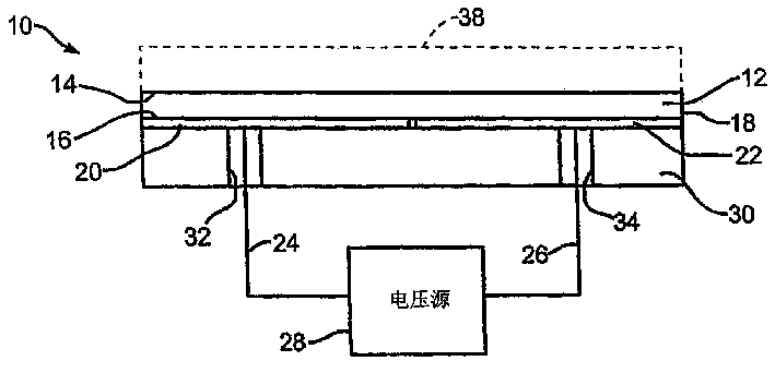
图1示出一基本的静电卡盘10,其包括根据本发明的一压盘12。压盘12由介电材料制成(现将作进一步详细描述),并具有如图1所示的上表面14和下表面16。压盘12的周缘18可以是如图2所示的圆形,以使压盘12具有一圆盘形状。一对电极20和22与压盘12的下表面16接触。电极20和22以一合适的方式附连于表面16,并通过引线24和26连接到一电压源28。电极的数量和形状纯粹是一设计选择的事情。与电极20、22接触的压盘12支承在电气绝缘材料的背板30上。引线24和26分别延伸通过背板30内的开口32和34。如图1所示,一待加工处理的半导体晶片38支承在压盘上表面14上。当要求将晶片38牢固地保持就位以便处理时,操作电压源28以在晶片38与压盘12之间施加一静电吸力,以便足够地将晶片38保持在卡盘10的一定位置上。晶片38的处理完成之后,停止施加电压源,以便允许晶片38从卡盘10中释放和移去。静电卡盘的这样的操作对于本技术领域内的技术人员都是熟知的。Figure 1 shows a basic
根据本发明的压盘12的特征在于呈绝缘体或Al2O3的薄层或类似的绝缘材料形式的新材料,其中,碳化、氮化转变的金属和/或导电的碳化颗粒进行扩散,即,用于静电卡盘的压盘的组合的陶瓷材料。这示于图3(a)-3(b)中,这些图是根据本发明的Al2O3-TiC复合物的扫描电子显微镜的照片,其中TiC的所占体积比例从2.5%变化到15%。The
本发明提供一种具有Al2O3的介电层的E形卡盘压盘,其中,由导电材料制成的颗粒以2.5至15%的体积含量扩散,这是一种典型的非常硬的陶瓷复合材料。Al2O3-TiC较佳地用于E形卡盘压盘材料。该材料(Al2O3-TiC)具有极佳的机械性能和静电夹紧能力。The present invention provides an E-shaped chuck platen with a dielectric layer of Al2O3 , in which particles made of conductive material are diffused at a volume content of 2.5 to 15%, which is a typical very hard ceramic composites. Al 2 O 3 -TiC is preferably used as the E-shaped chuck pressure plate material. The material (Al 2 O 3 -TiC) has excellent mechanical properties and electrostatic clamping ability.
根据本发明的静电卡盘压盘12由于如上所述的导电颗粒的扩散而具有一相当大的静电电容。这示于图4的表格中,它显示压盘12的Al2O3-TiC复合材料的电气特性。在根据本发明的E卡盘压盘12中,导电颗粒围绕多结晶的Al2O3的边界很好地扩散,以便实际地拓宽电极区域而增加了静电电容。与静电电容的增加成正比,在Al2O3-TiC的情形中的实际相对介电常数分别是增加TiC的24%和添加5%的TiC后的35%。The
根据本发明的压盘12的增加的静电电容导致一E卡盘压盘中的夹紧力显著地增加。因静电荷量的增加,本发明的E卡盘压盘12获得显著高的夹紧力。在Al2O3-TiC的情形中,具有0.3mm厚度的压盘的夹紧力分别在1500VDC(直流)下是44g/cm2,在1500VAC(交流)p-p(正、负峰间值)下是28g/cm2,与不包含TiC的Al2O3压盘的夹紧力相比它们增加60%和100%的夹紧力。这示于图5中的曲线50和52,图5是作为介电成分中TiC含量的函数的静电力的曲线。1500V的直流电压和1500V(Vp-p)的交流电压施加在空气中。介电层的厚度是0.3mm。The increased electrostatic capacitance of the
本发明的静电卡盘压盘12不管周围环境湿度如何能较佳地提供显著强的晶片夹紧力。图6(a)的曲线60和62示出了作为施加的直流电压的函数的静电力,而图6(b)的曲线64和66示出作为施加的交流电压(均方根值)的函数的静电力。图6(a)和6(b)的数据是用于包含在空气(相对湿度为46%)中的或氮气(相对湿度为46%)中的Al2O3+TiC的压盘12。压盘12的厚度从以上的信息中可得出是0.3mm。因此,本发明提供了一静电卡盘压盘12,其中,夹紧力在相对湿度从大约2%到40%的范围下具有足够的力来夹紧一晶片。The
本发明的压盘12还具有另外的特征:为了获得晶片的夹紧力施加到压盘上的电压可通过减小其介电层的厚度来减小。图7(a)的曲线70示出作为施加电压的函数的压盘材料的静电力,该压盘材料是0.3mm厚度的Al2O3+TiC5%。图7(b)的曲线72示出了作为施加电压的函数的0.1mm厚度的同一压盘材料的静电力。因此,压盘达到相同的夹紧力量,其施加的电压低达600V,介电层的厚度为0.1mm。The
本发明的静电卡盘压盘12上较佳地不具有残余电压。尤其是,通过将压盘的介电层厚度减小到0.1mm厚度,根据施加电压增加和/或减小的顺序留在压盘上的残余表面电势不保留在压盘上。这显示在图8和9的曲线中。The
图8(a)和8(b)示出作为空气中施加的电压的函数的表面电势,其用于具有0.3mm厚度的本发明的Al2O3+TiC5%的压盘材料。在电压施加到静电卡盘装置上之后,硅晶片从压盘剥下。曲线84示出表面电势对施加的电压的曲线,表征+1000V下的剥离,曲线86示出表面电势对施加的电压的曲线,表征-1000V下的剥离。图9(a)和9(b)示出关于具有0.1mm厚度的本发明的Al2O3+TiC5%的压盘材料的、作为在空气中施加的电压的函数的表面电势。在电压施加到静电卡盘装置上之后,硅晶片从压盘剥下。曲线88示出表面电势对施加的电压的曲线,表征+600V下的剥离,曲线90示出表面电势对施加的电压的曲线,表征-600V下的剥离。Figures 8(a) and 8(b) show the surface potential as a function of the applied voltage in air for the Al2O3 +TiC5% platen material of the invention having a thickness of 0.3 mm. After a voltage is applied to the electrostatic chuck device, the silicon wafer is peeled off from the platen.
根据本发明的压盘12具有一非常快的晶片释放能力,其原因在于先前所述的事实:为获得晶片夹紧力,施加到压盘12上的电压可通过减小介电层的厚度来减小。晶片的释放可在不到一秒的时间内实现,与介电层厚度未减小的晶片压盘相比残余夹紧力可减小约60%。图10(a)和10(b)的曲线示出了作为时间的函数的静电力,而曲线94和96分别代表0.3mm厚度和0.1mm厚度的、根据本发明的具有一压盘12的静电卡盘的释放响应(release response)。施加的电压在时间=0秒时关闭。显然,较快的释放响应对应于厚度减小的压盘12。The
具有减小了厚度的附加特征的本发明的压盘12提供一晶片夹紧力,在施加一直流电压或一等于直流电压的均方根值的交流电压的情形下具有相同的强度。图11(a)和11(b)示出了作为施加电压的函数的静电力,其中,曲线100是对于直流电压,而曲线102是对于交流电压(均方根值)。两者都是关于具有厚度为0.1mm的Al2O3+TiC5%的压盘12的静电卡盘。如曲线图所示,压盘12在施加到压盘的400V的直流电压和/或施加的400Vrms下,产生20g/cm2的晶片夹紧力。The
具有减小了厚度的附加特征的本发明的压盘12具有较小的对剪切力的力衰减比(与法向力,即沿垂直于表面14的方向的力比较)。图12(a)和12(b)中的曲线106和108分别示出沿剪切方向的静电力,其针对0.1mm厚度的Al2O3+TiC5%的压盘12,分别作为施加的直流电压和施加的交流电压(均方根值)的函数。压盘分别在施加直流电压下具有一66%的剪切力分量,在施加交流电压下具有一32%的剪切力分量(各与施加相同的直流电压和交流电压下的法向力比较)。The
除了上述的本发明的压盘12的特性之外,添加TiC可提供压盘12的如下理想的特性。一个是较高的硬度。Al2O3-TiC(30%TiC浓度)的硬度在摄氏500℃下的Vickers硬度约为1800,而在同样条件下Al2O3本身硬度是1600。因此,与Al2O3相比Al2O3-TiC的硬度要硬16%。硬度的增加有利于上述晶片压盘的较小的磨损特性,和/或由于材料磨损较小的特性对干净房间环境产生的污染也小。In addition to the characteristics of the
另一理想的特性是较高的温度转移特性。Al2O3-TiC(30%浓度)的传热比大约为21W/mK,而Al2O3本身在同样条件下为17W/mK。因此,与Al2O3相比Al2O3-TiC具有的传热指数(heat transfer characteristic)要好24%。较佳的传热特性有利于夹紧晶片在晶片的全部表面上热量的均匀分布。Another desirable property is higher temperature transfer properties. The heat transfer ratio of Al 2 O 3 -TiC (30% concentration) is about 21 W/mK, while Al 2 O 3 itself is 17 W/mK under the same conditions. Therefore, Al 2 O 3 —TiC has a heat transfer characteristic 24% better than Al 2 O 3 . The better heat transfer characteristics facilitate even distribution of heat over the entire surface of the wafer by clamping the wafer.
还有另一理想的特性是较高的抗断裂力。Al2O3-TiC(30%TiC浓度)的抗断裂力是700至800Mpa,而在同样条件下Al2O3本身是400至500MPa。因此,与Al2O3相比Al2O3-TiC具有高出60至70%的抗断裂力特性。较佳的抗断裂力特性有利于上述压盘的强度。Yet another desirable property is a high resistance to fracture. The fracture resistance of Al 2 O 3 -TiC (30% TiC concentration) is 700 to 800 MPa, while Al 2 O 3 itself is 400 to 500 MPa under the same conditions. Therefore, Al 2 O 3 —TiC has 60 to 70% higher fracture resistance characteristics than Al 2 O 3 . The preferred fracture force properties contribute to the strength of the platen as described above.
本发明的压盘12还具有良好的抗锈蚀、耐等离子和耐热特性。The
图13示出一根据本发明制作压盘的方法。在该方法的开始步骤120和12,分别提供介电陶瓷材料和导电材料。较佳地,介电陶瓷材料是颗粒大小约为0.2μm的氧化铝陶瓷粉末,而较佳地,导电陶瓷材料是具有约0.5μm的颗粒大小的碳化钛陶瓷粉末,并呈约从2.5%至15.0%的体积量。然后,在步骤124中两种材料在一溶剂(较佳地为酒精)中混合,时间持续约72小时。在步骤126中使合成的混合物干燥。定形步骤128包括将干燥的混合物定形或成形在一模具或类似的容器内。生成的形状要求对压盘来说是理想的,较佳地呈一圆盘的形式。然后,在下面的步骤130中,压盘在1600℃温度下和约20MPa的压力下烧结约一个小时。这可通过传统的热—压力过程来实施。烧结之后是打磨和抛光步骤132,主要在接触半导体晶片的压盘表面上进行处理。制成的压盘的厚度可在约0.1mm至2.0mm的范围内,依据不同的应用情况而定。步骤134代表制成的压盘,其呈一单层结构形式。Figure 13 shows a method of making a platen according to the present invention. In
尽管已经描述了本发明的一实施例,但这样做是为了说明的目的,而不是限制性的。While an embodiment of the invention has been described, this has been done for purposes of illustration and not limitation.
Claims (18)
Applications Claiming Priority (2)
| Application Number | Priority Date | Filing Date | Title |
|---|---|---|---|
| US10/137,790 | 2002-05-01 | ||
| US10/137,790 US6660665B2 (en) | 2002-05-01 | 2002-05-01 | Platen for electrostatic wafer clamping apparatus |
Publications (2)
| Publication Number | Publication Date |
|---|---|
| CN1663105A true CN1663105A (en) | 2005-08-31 |
| CN100508355C CN100508355C (en) | 2009-07-01 |
Family
ID=29269158
Family Applications (1)
| Application Number | Title | Priority Date | Filing Date |
|---|---|---|---|
| CNB038150476A Expired - Fee Related CN100508355C (en) | 2002-05-01 | 2003-04-30 | Improved platen for electrostatic wafer clamping device |
Country Status (9)
| Country | Link |
|---|---|
| US (1) | US6660665B2 (en) |
| EP (1) | EP1532728B1 (en) |
| JP (2) | JP5058438B2 (en) |
| KR (1) | KR100979684B1 (en) |
| CN (1) | CN100508355C (en) |
| AT (1) | ATE476782T1 (en) |
| AU (1) | AU2003228776A1 (en) |
| DE (1) | DE60333642D1 (en) |
| WO (1) | WO2003094335A1 (en) |
Cited By (3)
| Publication number | Priority date | Publication date | Assignee | Title |
|---|---|---|---|---|
| CN101221893B (en) * | 2007-01-12 | 2010-05-19 | 北京北方微电子基地设备工艺研究中心有限责任公司 | Method for promoting electrostatic charge dissipation on semiconductor chip |
| CN107206567A (en) * | 2014-11-23 | 2017-09-26 | M丘比德技术公司 | Wafer Pin Chuck Manufacturing and Repair |
| CN110491819A (en) * | 2018-05-14 | 2019-11-22 | 北京北方华创微电子装备有限公司 | The method and electrostatic chuck of equilibrium electrostatic power |
Families Citing this family (7)
| Publication number | Priority date | Publication date | Assignee | Title |
|---|---|---|---|---|
| JP4631748B2 (en) * | 2006-03-02 | 2011-02-16 | Toto株式会社 | Electrostatic adsorption method |
| JP4976911B2 (en) * | 2007-04-27 | 2012-07-18 | 新光電気工業株式会社 | Electrostatic chuck |
| US8363378B2 (en) * | 2009-02-17 | 2013-01-29 | Intevac, Inc. | Method for optimized removal of wafer from electrostatic chuck |
| JP6052976B2 (en) * | 2012-10-15 | 2016-12-27 | 日本タングステン株式会社 | Electrostatic chuck dielectric layer and electrostatic chuck |
| US20150062772A1 (en) * | 2013-08-27 | 2015-03-05 | Varian Semiconductor Equipment Associates, Inc | Barrier Layer For Electrostatic Chucks |
| JP7430489B2 (en) * | 2019-01-16 | 2024-02-13 | セメス株式会社 | Electrostatic chuck, electrostatic chuck device |
| KR102234220B1 (en) * | 2020-07-24 | 2021-03-30 | 이준호 | Conductive electrode static chuck lift pin, electrode static chuck including the same, and semiconductor production method using them |
Family Cites Families (16)
| Publication number | Priority date | Publication date | Assignee | Title |
|---|---|---|---|---|
| US3772748A (en) * | 1971-04-16 | 1973-11-20 | Nl Industries Inc | Method for forming electrodes and conductors |
| US4808315A (en) * | 1986-04-28 | 1989-02-28 | Asahi Kasei Kogyo Kabushiki Kaisha | Porous hollow fiber membrane and a method for the removal of a virus by using the same |
| JPH0521584A (en) * | 1991-07-16 | 1993-01-29 | Nikon Corp | Holding device |
| US5691876A (en) * | 1995-01-31 | 1997-11-25 | Applied Materials, Inc. | High temperature polyimide electrostatic chuck |
| JP3887842B2 (en) * | 1995-03-17 | 2007-02-28 | 東京エレクトロン株式会社 | Stage equipment |
| JPH0945753A (en) * | 1995-07-28 | 1997-02-14 | Kyocera Corp | Article holding device |
| US6399143B1 (en) * | 1996-04-09 | 2002-06-04 | Delsys Pharmaceutical Corporation | Method for clamping and electrostatically coating a substrate |
| US5754391A (en) * | 1996-05-17 | 1998-05-19 | Saphikon Inc. | Electrostatic chuck |
| JP4256483B2 (en) * | 1996-07-19 | 2009-04-22 | アプライド マテリアルズ インコーポレイテッド | Electrostatic chuck, apparatus for manufacturing integrated circuit device, and manufacturing method of electrostatic chuck |
| JPH11168134A (en) * | 1997-12-03 | 1999-06-22 | Shin Etsu Chem Co Ltd | Electrostatic suction device and method of manufacturing the same |
| US5969934A (en) * | 1998-04-10 | 1999-10-19 | Varian Semiconductor Equipment Associats, Inc. | Electrostatic wafer clamp having low particulate contamination of wafers |
| JP2000252351A (en) * | 1999-02-26 | 2000-09-14 | Taiheiyo Cement Corp | Electrostatic chuck and its manufacture |
| JP3805134B2 (en) * | 1999-05-25 | 2006-08-02 | 東陶機器株式会社 | Electrostatic chuck for insulating substrate adsorption |
| JP2002016129A (en) * | 2000-06-30 | 2002-01-18 | Taiheiyo Cement Corp | Electrostatic chuck |
| JP2002373769A (en) * | 2001-06-14 | 2002-12-26 | Ibiden Co Ltd | Hot plate unit |
| JP4510358B2 (en) * | 2002-03-27 | 2010-07-21 | 太平洋セメント株式会社 | Electrostatic chuck and manufacturing method thereof |
-
2002
- 2002-05-01 US US10/137,790 patent/US6660665B2/en not_active Expired - Lifetime
-
2003
- 2003-04-30 EP EP03726546A patent/EP1532728B1/en not_active Expired - Lifetime
- 2003-04-30 AT AT03726546T patent/ATE476782T1/en not_active IP Right Cessation
- 2003-04-30 WO PCT/US2003/013459 patent/WO2003094335A1/en not_active Ceased
- 2003-04-30 AU AU2003228776A patent/AU2003228776A1/en not_active Abandoned
- 2003-04-30 JP JP2004502453A patent/JP5058438B2/en not_active Expired - Fee Related
- 2003-04-30 KR KR1020047017606A patent/KR100979684B1/en not_active Expired - Lifetime
- 2003-04-30 CN CNB038150476A patent/CN100508355C/en not_active Expired - Fee Related
- 2003-04-30 DE DE60333642T patent/DE60333642D1/en not_active Expired - Lifetime
-
2011
- 2011-03-24 JP JP2011066529A patent/JP2011176328A/en active Pending
Cited By (3)
| Publication number | Priority date | Publication date | Assignee | Title |
|---|---|---|---|---|
| CN101221893B (en) * | 2007-01-12 | 2010-05-19 | 北京北方微电子基地设备工艺研究中心有限责任公司 | Method for promoting electrostatic charge dissipation on semiconductor chip |
| CN107206567A (en) * | 2014-11-23 | 2017-09-26 | M丘比德技术公司 | Wafer Pin Chuck Manufacturing and Repair |
| CN110491819A (en) * | 2018-05-14 | 2019-11-22 | 北京北方华创微电子装备有限公司 | The method and electrostatic chuck of equilibrium electrostatic power |
Also Published As
| Publication number | Publication date |
|---|---|
| WO2003094335A1 (en) | 2003-11-13 |
| US20030207596A1 (en) | 2003-11-06 |
| EP1532728A4 (en) | 2008-07-16 |
| HK1081735A1 (en) | 2006-05-19 |
| JP5058438B2 (en) | 2012-10-24 |
| KR100979684B1 (en) | 2010-09-02 |
| ATE476782T1 (en) | 2010-08-15 |
| US6660665B2 (en) | 2003-12-09 |
| AU2003228776A1 (en) | 2003-11-17 |
| JP2011176328A (en) | 2011-09-08 |
| JP2005524247A (en) | 2005-08-11 |
| DE60333642D1 (en) | 2010-09-16 |
| KR20050026385A (en) | 2005-03-15 |
| CN100508355C (en) | 2009-07-01 |
| EP1532728B1 (en) | 2010-08-04 |
| EP1532728A1 (en) | 2005-05-25 |
Similar Documents
| Publication | Publication Date | Title |
|---|---|---|
| JP4031732B2 (en) | Electrostatic chuck | |
| JP2011176328A (en) | Improved platen for electrostatic wafer clamping apparatus | |
| CN1365518A (en) | Electrostatic Chucks and Handling Devices | |
| CN112219273B (en) | Electrostatic chuck and method of manufacturing the same | |
| JP2001284442A (en) | Electrostatic chuck and method of manufacturing the same | |
| KR100450475B1 (en) | Electrostatic chucks and process for producing the same | |
| JP3586034B2 (en) | Electrostatic chuck | |
| JP3426845B2 (en) | Electrostatic chuck | |
| JP3447305B2 (en) | Electrostatic chuck | |
| JP3348140B2 (en) | Electrostatic chuck | |
| US20040121192A1 (en) | ALN material and electrostatic chuck incorporating same | |
| EP1513191A2 (en) | Heating apparatus having electrostatic adsorption function | |
| KR102822668B1 (en) | Dielectric for electrostatic chuck | |
| JP2000012666A (en) | Electrostatic chuck | |
| JP3370532B2 (en) | Electrostatic chuck | |
| JP3588253B2 (en) | Electrostatic chuck | |
| HK1081735B (en) | Improved platen for electrostatic wafer clamping apparatus | |
| JPH10189698A (en) | Electrostatic chuck | |
| JP3965469B2 (en) | Electrostatic chuck | |
| JP2002324832A (en) | Electrostatic chuck | |
| JP2000021963A (en) | Electrostatic suction device | |
| JPH03183151A (en) | Electrostatic chuck plate | |
| JP3527840B2 (en) | Electrostatic chuck | |
| JP2002324833A (en) | Electrostatic chuck | |
| Choi et al. | Ceramic electrode materials for electrostatic chuck applications |
Legal Events
| Date | Code | Title | Description |
|---|---|---|---|
| C06 | Publication | ||
| PB01 | Publication | ||
| C10 | Entry into substantive examination | ||
| SE01 | Entry into force of request for substantive examination | ||
| REG | Reference to a national code |
Ref country code: HK Ref legal event code: DE Ref document number: 1081735 Country of ref document: HK |
|
| C14 | Grant of patent or utility model | ||
| GR01 | Patent grant | ||
| REG | Reference to a national code |
Ref country code: HK Ref legal event code: GR Ref document number: 1081735 Country of ref document: HK |
|
| CF01 | Termination of patent right due to non-payment of annual fee | ||
| CF01 | Termination of patent right due to non-payment of annual fee |
Granted publication date: 20090701 Termination date: 20190430 |