EP1513191B1 - Heating apparatus having electrostatic adsorption function - Google Patents
Heating apparatus having electrostatic adsorption function Download PDFInfo
- Publication number
- EP1513191B1 EP1513191B1 EP04255100A EP04255100A EP1513191B1 EP 1513191 B1 EP1513191 B1 EP 1513191B1 EP 04255100 A EP04255100 A EP 04255100A EP 04255100 A EP04255100 A EP 04255100A EP 1513191 B1 EP1513191 B1 EP 1513191B1
- Authority
- EP
- European Patent Office
- Prior art keywords
- electrostatic adsorption
- insulating layer
- heating
- layer
- heating apparatus
- Prior art date
- Legal status (The legal status is an assumption and is not a legal conclusion. Google has not performed a legal analysis and makes no representation as to the accuracy of the status listed.)
- Expired - Fee Related
Links
- 238000010438 heat treatment Methods 0.000 title claims description 143
- 238000001179 sorption measurement Methods 0.000 title claims description 114
- 239000010410 layer Substances 0.000 claims description 174
- PZNSFCLAULLKQX-UHFFFAOYSA-N Boron nitride Chemical compound N#B PZNSFCLAULLKQX-UHFFFAOYSA-N 0.000 claims description 49
- 239000000758 substrate Substances 0.000 claims description 45
- OKTJSMMVPCPJKN-UHFFFAOYSA-N Carbon Chemical compound [C] OKTJSMMVPCPJKN-UHFFFAOYSA-N 0.000 claims description 35
- 239000011241 protective layer Substances 0.000 claims description 31
- 230000003746 surface roughness Effects 0.000 claims description 25
- 229910002804 graphite Inorganic materials 0.000 claims description 21
- 239000010439 graphite Substances 0.000 claims description 21
- 229910052799 carbon Inorganic materials 0.000 claims description 14
- 238000005229 chemical vapour deposition Methods 0.000 claims description 12
- PMHQVHHXPFUNSP-UHFFFAOYSA-M copper(1+);methylsulfanylmethane;bromide Chemical compound Br[Cu].CSC PMHQVHHXPFUNSP-UHFFFAOYSA-M 0.000 claims description 10
- 229910052582 BN Inorganic materials 0.000 claims description 7
- 229910052581 Si3N4 Inorganic materials 0.000 claims description 7
- PNEYBMLMFCGWSK-UHFFFAOYSA-N aluminium oxide Inorganic materials [O-2].[O-2].[O-2].[Al+3].[Al+3] PNEYBMLMFCGWSK-UHFFFAOYSA-N 0.000 claims description 7
- HQVNEWCFYHHQES-UHFFFAOYSA-N silicon nitride Chemical compound N12[Si]34N5[Si]62N3[Si]51N64 HQVNEWCFYHHQES-UHFFFAOYSA-N 0.000 claims description 7
- PCHJSUWPFVWCPO-UHFFFAOYSA-N gold Chemical compound [Au] PCHJSUWPFVWCPO-UHFFFAOYSA-N 0.000 claims description 6
- 229910052737 gold Inorganic materials 0.000 claims description 6
- 239000010931 gold Substances 0.000 claims description 6
- BASFCYQUMIYNBI-UHFFFAOYSA-N platinum Chemical group [Pt] BASFCYQUMIYNBI-UHFFFAOYSA-N 0.000 claims description 6
- 229910052709 silver Inorganic materials 0.000 claims description 6
- 239000004332 silver Substances 0.000 claims description 6
- 229910052796 boron Inorganic materials 0.000 claims description 5
- 238000007650 screen-printing Methods 0.000 claims description 5
- 229910052580 B4C Inorganic materials 0.000 claims description 3
- ZOXJGFHDIHLPTG-UHFFFAOYSA-N Boron Chemical compound [B] ZOXJGFHDIHLPTG-UHFFFAOYSA-N 0.000 claims description 3
- ZOKXTWBITQBERF-UHFFFAOYSA-N Molybdenum Chemical compound [Mo] ZOKXTWBITQBERF-UHFFFAOYSA-N 0.000 claims description 3
- BQCADISMDOOEFD-UHFFFAOYSA-N Silver Chemical compound [Ag] BQCADISMDOOEFD-UHFFFAOYSA-N 0.000 claims description 3
- RTAQQCXQSZGOHL-UHFFFAOYSA-N Titanium Chemical compound [Ti] RTAQQCXQSZGOHL-UHFFFAOYSA-N 0.000 claims description 3
- INAHAJYZKVIDIZ-UHFFFAOYSA-N boron carbide Chemical compound B12B3B4C32B41 INAHAJYZKVIDIZ-UHFFFAOYSA-N 0.000 claims description 3
- 239000000203 mixture Substances 0.000 claims description 3
- 229910052750 molybdenum Inorganic materials 0.000 claims description 3
- 239000011733 molybdenum Substances 0.000 claims description 3
- 229910052715 tantalum Inorganic materials 0.000 claims description 3
- GUVRBAGPIYLISA-UHFFFAOYSA-N tantalum atom Chemical compound [Ta] GUVRBAGPIYLISA-UHFFFAOYSA-N 0.000 claims description 3
- 229910052719 titanium Inorganic materials 0.000 claims description 3
- 239000010936 titanium Substances 0.000 claims description 3
- WFKWXMTUELFFGS-UHFFFAOYSA-N tungsten Chemical compound [W] WFKWXMTUELFFGS-UHFFFAOYSA-N 0.000 claims description 3
- 229910052721 tungsten Inorganic materials 0.000 claims description 3
- 239000010937 tungsten Substances 0.000 claims description 3
- 235000012431 wafers Nutrition 0.000 description 120
- XUIMIQQOPSSXEZ-UHFFFAOYSA-N Silicon Chemical compound [Si] XUIMIQQOPSSXEZ-UHFFFAOYSA-N 0.000 description 88
- 229910052710 silicon Inorganic materials 0.000 description 88
- 239000010703 silicon Substances 0.000 description 88
- 239000002245 particle Substances 0.000 description 32
- 239000000463 material Substances 0.000 description 22
- 238000000034 method Methods 0.000 description 22
- 230000008569 process Effects 0.000 description 18
- 239000007789 gas Substances 0.000 description 17
- QGZKDVFQNNGYKY-UHFFFAOYSA-N Ammonia Chemical compound N QGZKDVFQNNGYKY-UHFFFAOYSA-N 0.000 description 14
- 238000001816 cooling Methods 0.000 description 13
- 239000004065 semiconductor Substances 0.000 description 13
- 238000002474 experimental method Methods 0.000 description 12
- 238000004519 manufacturing process Methods 0.000 description 11
- VNWKTOKETHGBQD-UHFFFAOYSA-N methane Chemical compound C VNWKTOKETHGBQD-UHFFFAOYSA-N 0.000 description 8
- 229910021529 ammonia Inorganic materials 0.000 description 7
- 238000000227 grinding Methods 0.000 description 6
- 238000005498 polishing Methods 0.000 description 6
- 239000000919 ceramic Substances 0.000 description 5
- -1 sialon Chemical compound 0.000 description 5
- FAQYAMRNWDIXMY-UHFFFAOYSA-N trichloroborane Chemical compound ClB(Cl)Cl FAQYAMRNWDIXMY-UHFFFAOYSA-N 0.000 description 5
- 230000015572 biosynthetic process Effects 0.000 description 4
- 238000006243 chemical reaction Methods 0.000 description 4
- 239000012535 impurity Substances 0.000 description 4
- 238000011109 contamination Methods 0.000 description 3
- 230000005611 electricity Effects 0.000 description 3
- 238000005530 etching Methods 0.000 description 3
- 238000012545 processing Methods 0.000 description 3
- 230000002411 adverse Effects 0.000 description 2
- 238000000137 annealing Methods 0.000 description 2
- 230000015556 catabolic process Effects 0.000 description 2
- 230000000052 comparative effect Effects 0.000 description 2
- 230000000694 effects Effects 0.000 description 2
- 230000020169 heat generation Effects 0.000 description 2
- 229910052751 metal Inorganic materials 0.000 description 2
- 239000002184 metal Substances 0.000 description 2
- 230000003287 optical effect Effects 0.000 description 2
- 230000000704 physical effect Effects 0.000 description 2
- 230000000630 rising effect Effects 0.000 description 2
- 239000002344 surface layer Substances 0.000 description 2
- 238000012546 transfer Methods 0.000 description 2
- 230000009471 action Effects 0.000 description 1
- 230000008901 benefit Effects 0.000 description 1
- 230000008602 contraction Effects 0.000 description 1
- 239000013078 crystal Substances 0.000 description 1
- 230000003247 decreasing effect Effects 0.000 description 1
- 230000007547 defect Effects 0.000 description 1
- 230000000593 degrading effect Effects 0.000 description 1
- 238000004299 exfoliation Methods 0.000 description 1
- 239000010408 film Substances 0.000 description 1
- 230000006872 improvement Effects 0.000 description 1
- 238000007689 inspection Methods 0.000 description 1
- 239000011810 insulating material Substances 0.000 description 1
- 238000009413 insulation Methods 0.000 description 1
- 238000011835 investigation Methods 0.000 description 1
- 230000003647 oxidation Effects 0.000 description 1
- 238000007254 oxidation reaction Methods 0.000 description 1
- 229920005989 resin Polymers 0.000 description 1
- 239000011347 resin Substances 0.000 description 1
- 238000004544 sputter deposition Methods 0.000 description 1
- 239000010409 thin film Substances 0.000 description 1
Images
Classifications
-
- H—ELECTRICITY
- H01—ELECTRIC ELEMENTS
- H01L—SEMICONDUCTOR DEVICES NOT COVERED BY CLASS H10
- H01L21/00—Processes or apparatus adapted for the manufacture or treatment of semiconductor or solid state devices or of parts thereof
- H01L21/67—Apparatus specially adapted for handling semiconductor or electric solid state devices during manufacture or treatment thereof; Apparatus specially adapted for handling wafers during manufacture or treatment of semiconductor or electric solid state devices or components ; Apparatus not specifically provided for elsewhere
- H01L21/683—Apparatus specially adapted for handling semiconductor or electric solid state devices during manufacture or treatment thereof; Apparatus specially adapted for handling wafers during manufacture or treatment of semiconductor or electric solid state devices or components ; Apparatus not specifically provided for elsewhere for supporting or gripping
- H01L21/687—Apparatus specially adapted for handling semiconductor or electric solid state devices during manufacture or treatment thereof; Apparatus specially adapted for handling wafers during manufacture or treatment of semiconductor or electric solid state devices or components ; Apparatus not specifically provided for elsewhere for supporting or gripping using mechanical means, e.g. chucks, clamps or pinches
- H01L21/68714—Apparatus specially adapted for handling semiconductor or electric solid state devices during manufacture or treatment thereof; Apparatus specially adapted for handling wafers during manufacture or treatment of semiconductor or electric solid state devices or components ; Apparatus not specifically provided for elsewhere for supporting or gripping using mechanical means, e.g. chucks, clamps or pinches the wafers being placed on a susceptor, stage or support
- H01L21/68757—Apparatus specially adapted for handling semiconductor or electric solid state devices during manufacture or treatment thereof; Apparatus specially adapted for handling wafers during manufacture or treatment of semiconductor or electric solid state devices or components ; Apparatus not specifically provided for elsewhere for supporting or gripping using mechanical means, e.g. chucks, clamps or pinches the wafers being placed on a susceptor, stage or support characterised by a coating or a hardness or a material
-
- H—ELECTRICITY
- H01—ELECTRIC ELEMENTS
- H01L—SEMICONDUCTOR DEVICES NOT COVERED BY CLASS H10
- H01L21/00—Processes or apparatus adapted for the manufacture or treatment of semiconductor or solid state devices or of parts thereof
- H01L21/67—Apparatus specially adapted for handling semiconductor or electric solid state devices during manufacture or treatment thereof; Apparatus specially adapted for handling wafers during manufacture or treatment of semiconductor or electric solid state devices or components ; Apparatus not specifically provided for elsewhere
- H01L21/67005—Apparatus not specifically provided for elsewhere
- H01L21/67011—Apparatus for manufacture or treatment
- H01L21/67098—Apparatus for thermal treatment
- H01L21/67103—Apparatus for thermal treatment mainly by conduction
-
- H—ELECTRICITY
- H01—ELECTRIC ELEMENTS
- H01L—SEMICONDUCTOR DEVICES NOT COVERED BY CLASS H10
- H01L21/00—Processes or apparatus adapted for the manufacture or treatment of semiconductor or solid state devices or of parts thereof
- H01L21/67—Apparatus specially adapted for handling semiconductor or electric solid state devices during manufacture or treatment thereof; Apparatus specially adapted for handling wafers during manufacture or treatment of semiconductor or electric solid state devices or components ; Apparatus not specifically provided for elsewhere
- H01L21/683—Apparatus specially adapted for handling semiconductor or electric solid state devices during manufacture or treatment thereof; Apparatus specially adapted for handling wafers during manufacture or treatment of semiconductor or electric solid state devices or components ; Apparatus not specifically provided for elsewhere for supporting or gripping
- H01L21/6831—Apparatus specially adapted for handling semiconductor or electric solid state devices during manufacture or treatment thereof; Apparatus specially adapted for handling wafers during manufacture or treatment of semiconductor or electric solid state devices or components ; Apparatus not specifically provided for elsewhere for supporting or gripping using electrostatic chucks
- H01L21/6833—Details of electrostatic chucks
Definitions
- the present invention relates to a heating apparatus having an electrostatic adsorption function, and specifically to a heating apparatus having an electrostatic adsorption function which is used suitably for a heating process of a semiconductor wafer, including a temperature rising process, in the production process and the inspection process of a semiconductor device or the like.
- an electrostatically adsorbing apparatus is used in a reduced pressure atmosphere for fixing a semiconductor wafer on a heater when heating the semiconductor wafer, and the material therefor has shifted to ceramics from resins with a tendency of higher temperature processes (see Japanese Patent Applications Laid-Open (Kokai) No. 52-67353 and No. 59-124140 ).
- wafer heating apparatuses having electrostatic adsorption functions wherein the wafer heating apparatus united with ceramics and the electrostatically adsorbing apparatus are combined.
- an apparatus wherein alumina is employed for an insulating layer of the electrostatically adsorbing apparatus is used in a low-temperature range such as an etching process (see New ceramics (7), p49-53, 1994 .).
- an apparatus, wherein silicon nitride, sialon, or aluminum nitride is employed for an insulating layer of the electrostatically adsorbing apparatus (see Japanese Patent Application Laid-Open (Kokai) No.
- Such a heating apparatus having the electric adsorption function is set and used in a semiconductor process chamber. For example, when heating a silicon wafer by using this heating apparatus having the electric adsorption function, first, a silicon wafer is carried into the process chamber with a transfer arm, and the silicon wafer is placed on the heating apparatus having the electrostatic adsorption function.
- the silicon wafer is heated by charging a heating layer with electricity while the silicon wafer is adsorbed to the heating apparatus by applying a voltage to an electrode for electrostatic adsorption. After the silicon wafer is heated to a predetermined temperature, processes of annealing and etching, or growing a film by sputtering, CVD or the like are performed.
- the power supply for the heating layer is turned off so that the silicon wafer is cooled.
- the power supply for the electrode for electrostatic adsorption is turned off, and the silicon wafer are pulled by using a lift pin or the like from the heating apparatus having the electrostatic adsorption function. After that, the silicon wafer is carried outside the process chamber with the transfer arm.
- Vickers hardness of the silicon wafer is about 11 GPa
- Vickers hardness of alumina, silicon nitride, sialon, and aluminum nitride, which are used as a material of the insulating layer are 15 GPa, 16 GPa, 16 GPa, and 14 GPa, respectively.
- the heating apparatus having the electrostatic adsorption function wherein alumina, silicon nitride, sialon, or aluminum nitride which are harder than the silicon wafer is used for the insulating layer, there is the problem that the surface of the silicon wafer is ground by the insulating layer when heating/cooling the silicon wafer, then particles are generated, and moreover, scratches are generated on the surface of the silicon wafer.
- the difference in thermal expansion volume between the insulating layer and the silicon wafer is further increased, so the particles are further easily generated, and moreover, the scratches are remarkably generated on the surface of the silicon wafer, so that the flatness of the silicon wafer is degraded.
- the particles are generated in the processes such as annealing and etching, it causes the generation of pattern defects and the like in the subsequent device fabrication process, and leads to various problems such as lowering device yield and degrading reliability of devices.
- pyrolytic boron nitride has small Vickers hardness of 2 GPa, which is softer than the silicon wafer. Therefore, there are few cases that the surface of the silicon wafer is ground by the insulating layer when heating/cooling the silicon wafer as described above. But on the contrary, there is the problem that the surface of the insulating layer is ground by the silicon wafer, so that the particles are generated as in the above.
- An object of the present invention is to provide a heating apparatus having an electrostatic adsorption function in which scratches are not generated on a silicon wafer or the like and the generation of particles can be suppressed when heating/cooling the wafer and the like.
- a heating apparatus having an electrostatic adsorption function, comprising at least a supporting substrate, an electrode for electrostatic adsorption and a heating layer formed on the supporting substrate, and an insulating layer formed so as to cover the electrode for electrostatic adsorption and the heating layer, wherein a surface roughness of the insulating layer satisfies Ra ⁇ 0.05 ⁇ m and Rmax ⁇ 0.6 ⁇ m, and Vickers hardness of the surface of the insulating layer is 10 GPa or less, according to claim 1.
- the heating apparatus having an electrostatic adsorption function comprising at least a supporting substrate, an electrode for electrostatic adsorption, a heating layer, and an insulating layer, if an average surface roughness of the insulating layer satisfies Ra ⁇ 0.05 ⁇ m and a maximum surface roughness thereof satisfies Rmax ⁇ 0.6 ⁇ m, and Vickers hardness of the surface of the insulating layer is 10 GPa or less, since Vickers hardness of the insulating layer is smaller than that of a silicon wafer, for example, the silicon wafer is not ground by the insulating layer even though they rub against each other due to the difference in each thermal expansion when heating/cooling the silicon wafer.
- a heating apparatus having an electrostatic adsorption function in which the generation of scratches on the wafer surface and the insulating layer can be prevented and the generation of particles can be suppressed.
- the insulating layer consists of pyrolytic boron nitride or pyrolytic boron nitride containing carbon.
- the insulating layer consists of pyrolytic boron nitride, since Vickers hardness of pyrolytic boron nitride is smaller than that of the silicon wafer, the silicon wafer is not ground by the insulating layer even though they rub against each other when heating/cooling the silicon wafer, and therefore, the generation of scratches and particles due to grinding the silicon wafer can be surely prevented.
- the insulating layer consists of pyrolytic boron nitride containing carbon
- Vickers hardness of pyrolytic boron nitride containing carbon is smaller than that of the silicon wafer, but larger than that of pure pyrolytic boron nitride, that is, can be closer to that of the silicon wafer, the generation of scratches on the wafer can be prevented, and since the insulating layer is difficult to be ground, the generation of particles can be further suppressed.
- the insulating layer has a thickness of 50-500 ⁇ m.
- the insulating layer of the heating apparatus has such a thickness, sufficient electrostatic adsorption power can be obtained without the generation of dielectric breakdown when applying a voltage to the electrode for electrostatic adsorption, and therefore, the wafer can be stably adsorbed electrostatically.
- the electrode for electrostatic adsorption and the heating layer are formed on a protective layer formed on the supporting substrate.
- the electrode for electrostatic adsorption and the heating layer are formed on a protective layer formed on the supporting substrate, contamination due to impurities, gases, and so on contained in the supporting substrate can be surely prevented.
- the protective layer consists of pyrolytic boron nitride.
- the protective layer consisting of pyrolytic boron nitride is formed on the supporting substrate, the protective layer can be stable even in a high temperature, and do not exfoliate.
- the supporting substrate consists of any one of a silicon nitride sintered body, a boron nitride sintered body, a mixed sintered body of boron nitride and aluminum nitride, an alumina sintered body, an aluminum nitride sintered body, and graphite.
- the supporting substrate consists of such a material, since it is excellent in physical properties such as heat resistance and strength, there can be obtained the heating apparatus possible to use stably for a long time.
- the electrode for electrostatic adsorption and/or the heating layer consist of any one of gold, the platinum group, silver, a mixture of gold or the platinum group and silver, titanium, tungsten, tantalum, molybdenum, pyrolytic graphite, and pyrolytic graphite containing boron and/or boron carbide.
- the electrode for electrostatic adsorption consists of the above materials
- the electrode can be easily formed and the wafer can be electrostatically adsorbed suitably.
- the heating layer consists of the above materials, the heating layer can be easily formed and the heat generation can be performed efficiently without causing troubles such as a thermal deformation, a disconnection, and a short circuit.
- the electrode for electrostatic adsorption and/or the heating layer are formed by screen printing or chemical vapor deposition.
- the electrode for electrostatic adsorption and/or the heating layer are formed by screen printing or chemical vapor deposition, they can be formed in a desired thickness uniformly on the supporting substrate or the protective layer. And moreover, the bonding strength between the electrode for electrostatic adsorption or the heating layer and the supporting substrate (or the protective layer) and the bonding strength between the electrode for electrostatic adsorption or the heating layer and the insulating layer formed thereon can get further strong.
- the heating apparatus having an electrostatic adsorption function of the present invention even when a silicon wafer is subjected to the device fabrication process or the like in a medium and high temperature range of 500-800°C, for example, scratches are not generated on the surface of the silicon wafer, and the generation of particles can be suppressed. Therefore, by using the heating apparatus having the electrostatic adsorption function of the present invention, the reliability and yield of a semiconductor device in the device fabrication process and the like can be extremely improved.
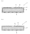
- Fig. 1 is a schematic sectional view showing an example of a heating apparatus having an electrostatic adsorption function of the present invention.
- the heating apparatus having an electrostatic adsorption function 1 an electrode for electrostatic adsorption 4 and a heating layer 5 are formed on a protective layer 3 formed on a supporting substrate 2 having a circular plate shape.
- an insulating layer 6 is formed so as to cover the electrode for electrostatic adsorption 4 and the heating layer 5.
- a power feeding terminal for the electrostatic adsorption and a power feeding terminal for the heating layer for the connection to an external power supply are provided with the electrode for electrostatic adsorption 4 and the heating layer 5, respectively, and electricity is supplied through the terminals to each of them.
- the semiconductor wafer When heating a semiconductor wafer and the like, by supplying electricity from the power feeding terminal for the electrostatic adsorption and the power feeding terminal for the heating layer provided with the electrode for electrostatic adsorption 4 and the heating layer 5, respectively, the semiconductor wafer can be adsorbed and fixed on the insulating layer 6 on the front surface of the supporting substrate 2 by the electrode for electrostatic adsorption 4, and the wafer can be heated by the conductive heating layer 5 on the back surface of the supporting substrate 2.
- the material of the supporting substrate 2 is not limited particularly, it is preferable that the supporting substrate 2 consists of any one of silicon nitride sintered body, boron nitride sintered body, mixed sintered body of boron nitride and aluminum nitride, alumina sintered body, aluminum nitride sintered body, and graphite. If the supporting substrate 2 consists of such a material, since each material is inexpensive and has excellent physical properties such as heat resistance and strength, there can be desirably obtained the heating apparatus possible to use stably for a long time even when heating/cooling is repeated in the medium and high temperature range of 500-800°C, for example.
- the shape of the supporting substrate 2 is not limited particularly, and besides the circular plate shape as described above, it may be a polygonal plate shape, a cylindrical shape, a shape of a circular plate or a cylinder with concave or convex portions, or the like.
- a protective layer 3 is essential to secure the insulation performance and also necessary to prevent the oxidation in the case that the supporting substrate 2 consists of graphite, for example.
- the supporting substrate 2 consists of an insulating material and the like, there can be provided a heating apparatus 11 having an electrostatic adsorption function without forming the protective layer 3 as shown in Fig. 2 , for example.
- the contamination due to impurities and the like contained in the sintered body as described above, for example can be surely prevented if the protective layer 3 is formed.
- the material of the protective layer 3 has stability up to a high temperature. Silicon nitride, boron nitride, alumina, aluminum nitride, pyrolytic boron nitride, and the like can be given as examples. Particularly, when the protective layer 3 consists of pyrolytic boron nitride, it is preferable because the protective layer is stable up to high temperature of 1500°C or more. Further, as to the thickness of the protective layer 3, if the layer is too thick, the exfoliation occurs easily due to the difference in thermal expansion between the supporting substrate and the protective layer, and if the layer is too thin, impurities, gases and the like pass through pin holes of the layer, which may adversely affect the subsequent fabrication process. Therefore, it is desirable that the protective layer is formed with the thickness of about 10-300 ⁇ m, in particular, about 30-150 ⁇ m.
- each material of the electrode for electrostatic adsorption 4 and the heating layer 5 is not limited particularly, it is preferable that the electrode for electrostatic adsorption 4 and the heating layer 5 consist of any one of gold, the platinum group, silver, a mixture of gold or the platinum group and silver, titanium, tungsten, tantalum, molybdenum, pyrolytic graphite, and pyrolytic graphite containing boron and/or boron carbide.
- the electrode for electrostatic adsorption 4 consists of such materials, since the electrode can be easily formed and an electrostatic adsorption power is high in a middle and high temperature range, a wafer can be electrostatically adsorbed suitably.
- the heating layer 5 consists of the materials as described above, the heating layer can be easily formed and the heat generation can be performed efficiently without causing troubles such as a thermal deformation, a disconnection, and a short circuit.
- each thickness of the electrode for electrostatic adsorption 4 and the heating layer 5 is not limited particularly, it is desirably 10-300 ⁇ m, in particular, 30-150 ⁇ m.
- an object to be heated such as a semiconductor wafer can be electrostatically adsorbed suitably and heated effectively.
- the surface roughness of the insulating layer satisfies Ra ⁇ 0.05 ⁇ m and Rmax ⁇ 0.6 ⁇ m, there are only a few and small protrusions on the surface of the insulating layer to be in contact with a silicon wafer, and thereby, even if the wafer and the insulating layer rub against each other due to the difference in each thermal expansion when heating/cooling the wafer, each of the wafer and the insulating layer is difficult to be ground each other, and thus generation of particles can be suppressed.
- Vickers hardness of the surface of the insulating layer is 10 GPa or less, which is less than that of a silicon wafer, even if they rub against each other when heating/cooling the silicon wafer, the silicon wafer is not ground, and thus, generation of scratches on the wafer surface can be surely prevented.
- the Vickers hardness of the surface of the insulating layer is too small, it is considered that since the insulating layer is soft, generation of the particles can not be sufficiently suppressed even when the surface roughness of the insulating layer is controlled as described above. Therefore, it is preferable that the Vickers hardness of the surface of the insulating layer is 0.5 GPa or more.
- the insulating layer 6 has the thickness of 50-500 ⁇ m, in particular, 100-200 ⁇ m. If the insulating layer 6 has the thickness of less than 50 ⁇ m, there is a possibility that dielectric breakdown occurs in the insulating layer. On the other hand, if the insulating layer has the thickness of more than 500 ⁇ m, there is a possibility that sufficient electrostatic adsorption power can not be obtained.
- the insulating layer 6 consists of pyrolytic boron nitride or pyrolytic boron nitride containing carbon.
- pyrolytic boron nitride as a material of the insulating layer 6, Vickers hardness of pyrolytic boron nitride is about 2 GPa in general, which is smaller than that of a silicon wafer (generally 11 GPa). Therefore, even in the case that the insulating layer and the silicon wafer rub against each other when heating/cooling the silicon wafer, particles and scratches generated by the silicon wafer being ground can be surely prevented.
- the insulating layer consists of pyrolytic boron nitride containing carbon
- Vickers hardness of pyrolytic boron nitride containing carbon is about 3 GPa, which is smaller than that of a silicon wafer, but larger than that of pure pyrolytic boron nitride, i.e., can be closer to that of the silicon wafer. Therefore, generation of scratches on the wafer surface can be surely prevented, and moreover, since the insulating layer is difficult to be ground, generation of particles can be further suppressed.
- a heating apparatus 1 having an electrostatic adsorption function As an insulating layer 6 of a heating apparatus 1 having an electrostatic adsorption function as shown in Fig. 1 , several kinds of heating apparatuses having an electrostatic adsorption function, having different surface roughness within the range of 0.03 ⁇ m ⁇ Ra ⁇ 0.07 ⁇ m and 0.4 ⁇ m ⁇ Rmax ⁇ 0.8 ⁇ m on each insulating layer consisting of pyrolytic boron nitride containing carbon, were prepared. In this case, each Vickers hardness of the surfaces of the insulating layers was 3 GPa.
- each surface (adsorbed surface) of the silicon wafers which had been heated/cooled by each heating apparatus was measured by a particle counter, and the number of particles having the size of 0.2 ⁇ m or more was counted.
- Table 1 Samples Surface roughness of insulating layer Number of particles having the size of 0.2 ⁇ m or more (numbers) Ra( ⁇ m) Rmax ( ⁇ m) Experiment 1 0.03 0.6 5900 Experiment 2 0.05 0.6 7000 Experiment 3 0.07 0.6 12900 Experiment 4 0.04 0.4 6000 Experiment 5 0.04 0.6 6500 Experiment 6 0.04 0.8 13400
- the heating apparatus having an electrostatic adsorption function of the present invention there is provided the heating apparatus having an electrostatic adsorption function in which even if the insulating layer and the silicon wafer rub against each other when heating/cooling the silicon wafer or the like in a medium and high temperature range of 500-800°C, for example, the silicon wafer is not ground, so that particles generated from the silicon wafer and the generation of scratches on the wafer surface can be surely prevented and the generation of particles by the insulating layer being ground can be suppressed. Therefore, by using the heating apparatus having the electrostatic adsorption function of the present invention in the device fabrication process and the like, the heating apparatus can greatly contribute to the improvement of reliability and yield of a semiconductor device.
- the heating apparatus having the electrostatic adsorption function of the present invention is effective if the surface roughness of the insulating layer satisfies Ra ⁇ 0.05 ⁇ m and Rmax ⁇ 0.6 ⁇ m, and Vickers hardness of the surface of the insulating layer is 10 GPa or less as mentioned above, and therefore, when it is necessary to form an insulating layer having Vickers hardness larger than that of a silicon wafer, by further forming a surface layer having Vickers hardness of 10 GPa or less on the insulating layer and controlling the surface roughness of the surface layer within the above range, there can also be provided the heating apparatus in which scratches are not generated on the silicon wafer and the generation of particles can be suppressed.
- a protective layer 3 is formed on a supporting substrate 2 as needed.
- a protective layer consisting of pyrolytic boron nitride can be formed on the supporting substrate consisting of graphite by reacting a mixed gas of ammonia and boron trichloride under a predetermined temperature and a predetermined pressure.
- an electrode for electrostatic adsorption 4 and a heating layer 5 are formed.
- the electrode for electrostatic adsorption 4 and the heating layer 5 can be easily formed by screen printing or chemical vapor deposition.
- a pyrolytic graphite layer is formed on the protective layer by reacting a methane gas under the condition of 1000-2500°C and 1-10 Torr, and subsequently a pattern of the electrode for electrostatic adsorption 4 is processed in the pyrolytic graphite layer on the front surface of the supporting substrate and the pattern of the heating layer 5 is processed in the pyrolytic graphite layer on the back surface thereof.
- the electrode for electrostatic adsorption and the heating layer can be formed uniformly on the supporting substrate or the protective layer with a desired thickness and a high adhesiveness, and the bonding strength between the electrode or the heating layer and the insulating layer formed thereon is further strengthened.
- the electrode for electrostatic adsorption and the heating layer by the screen printing, a high bonding strength between the electrode or the heating layer and the insulating layer can be obtained as in the chemical vapor deposition and additionally, it is not necessary to perform a pattern processing for the electrode for electrostatic adsorption and the heating layer, so that there is an advantage that the production processes can be reduced, and thus, the electrode for electrostatic adsorption and the heating layer can be easily formed.
- the protective layer is not needed depending on the material of the supporting layer or the like, it is possible to form the electrode for electrostatic adsorption 4 and the heating layer 5 directly on the supporting substrate 2, as in the heating apparatus 11 having the electrostatic adsorption function shown in Fig. 2 .
- an insulating layer 6 is formed on the electrode for electrostatic adsorption 4 and the heating layer 5.
- Vickers hardness of the surface of the insulating layer is adjusted to 10 GPa or less, which is surely less than that of a silicon wafer (generally about 11 GPa).
- Vickers hardness of the insulating layer depends on the material and formation method thereof, or the like. Therefore, in order to adjust Vickers hardness of the surface of the insulating layer to 10 GPa or less, the material and formation method of the insulating layer can be properly selected, and if the insulating layer having Vickers hardness of 10 GPa or less can be formed, the formation method thereof is not limited particularly, and thus, the formation method suitable for the material can be used.
- the insulating layer 6 can be preferably formed by chemical vapor deposition using the material gases for forming pyrolytic boron nitride.
- the chemical vapor deposition is performed with the gases of ammonia and boron halide under the condition of 1600-2000°C and 5-100 Torr, the insulating layer consisting of pyrolytic boron nitride in which Vickers hardness of the surface is 10 GPa or less can be easily formed.
- the material of the insulating layer 6 is pyrolytic boron nitride containing carbon
- the insulating layer can be preferably formed.
- the chemical vapor deposition is performed with the gases of ammonia, boron halide, and methane under the condition of 1600-2000°C and 5-100 Torr, the insulating layer consisting of pyrolytic boron nitride containing carbon in which Vickers hardness of the surface is 10 GPa or less can be easily formed.
- the surface of the insulating layer is subjected to surface grinding, mirror polishing and the like, and thereby, the insulating layer has the surface roughness of Ra ⁇ 0.05 ⁇ m and Rmax ⁇ 0.6 ⁇ m.
- processing conditions of the surface grinding or the mirror polishing are not limited particularly, and it is possible to perform the grinding and the polishing under the proper condition so that the surface roughness of the insulating layer is within the above ranges.
- an heating apparatus having an electrostatic adsorption function comprising at least a supporting substrate, an electrode for electrostatic adsorption and a heating layer formed on the supporting substrate, and an insulating layer formed so as to cover the electrode for electrostatic adsorption and the heating layer, wherein a surface roughness of the insulating layer satisfies Ra ⁇ 0.05 ⁇ m and Rmax ⁇ 0.6 ⁇ m, and Vickers hardness of the surface of the insulating layer is 10 GPa or less.
- a graphite substrate having a diameter of 200 mm and a thickness of 15 mm was prepared as a supporting substrate, and the reaction of a mixed gas of ammonia and boron trichloride was performed thereto under the condition of 1800°C and 100 Torr to form a protective layer consisting of pyrolytic boron nitride on the supporting substrate.
- methane gas was pyrolyzed on the protective layer under the condition of 2200°C and 5 Torr to form a pyrolytic graphite layer having a thickness of 100 ⁇ m.
- the front surface of the pyrolytic graphite layer was processed into an electrode pattern to form an electrode for electrostatic adsorption, and the back surface thereof was processed into a heater pattern to form a heating layer.
- the reaction of a mixed gas of the gas containing ammonia and boron trichloride with methane was further performed under the condition of 2000°C and 100 Torr to form an insulating layer consisting of pyrolytic boron nitride containing carbon having a thickness of 200 ⁇ m.
- a heating apparatus having an electrostatic adsorption function was manufactured.
- heating apparatus having the electrostatic adsorption function was set in the vacuum chamber and a silicon wafer having a diameter of 200 mm was placed on the heating apparatus, a voltage was applied to the electrode for electrostatic adsorption and the heating layer was electrically charged, then the silicon wafer was heated to 800°C and cooled while adsorbing the silicon wafer at an adsorption power of 3 g/cm. After the silicon wafer was cooled, the silicon wafer was taken out from the vacuum chamber.
- the adsorbed surface of the silicon wafer was measured by the particle counter, and the number of particles having the size of 0.2 ⁇ m or more was counted. As a result, the number of the particles on the surface of the silicon wafer was 7000. Also, the surface of the silicon wafer was observed by the optical microscope, and no scratch to be generated by rubbing against the surfaces of the wafer and the insulating layer was observed on the wafer surface.
- a graphite substrate having a diameter of 200 mm and a thickness of 15 mm was prepared as a supporting substrate, and a protective layer consisting of pyrolytic boron nitride was formed on the supporting substrate as in the above Example 1, and subsequently, an electrode for electrostatic adsorption and a heating layer were formed on the protective layer.
- the reaction of a gas containing ammonia and boron trichloride was performed under the condition of 1800°C and 100 Torr to form an insulating layer consisting of pyrolytic boron nitride having a thickness of 200 ⁇ m. Thereby, a heating apparatus having an electrostatic adsorption function was manufactured.
- the silicon wafer was heated to 800°C and cooled while adsorbing the silicon wafer at an adsorption power of 3 g/cm, as in the above Example 1. After the silicon wafer was cooled, the silicon wafer was taken out from the vacuum chamber. After that, an adsorbed surface of the silicon wafer was measured by the particle counter, and the number of particles having the size of 0.2 ⁇ m or more was counted. As a result, the number of the particles on the surface of the silicon wafer was 10000. Also, the surface of the silicon wafer was observed by the optical microscope, and as a result, no scratch was observed on the wafer surface.
- a graphite substrate having a diameter of 200 mm and a thickness of 15 mm was prepared as a supporting substrate, and a protective layer consisting of pyrolytic boron nitride was formed on the supporting substrate as in the above Example 2, and subsequently, an electrode for electrostatic adsorption and a heating layer were formed on the protective layer.
- the reaction of a gas containing ammonia and boron trichloride was performed under the condition of 1800°C and 100 Torr to form an insulating layer consisting of pyrolytic boron nitride having a thickness of 200 ⁇ m as in the above Example 2.
- the silicon wafer was heated to 800°C and cooled while adsorbing the silicon wafer at an adsorption power of 3 g/cm. After the silicon wafer was cooled, the silicon wafer was taken out from the vacuum chamber. After that, the adsorbed surface of the silicon wafer was measured by the particle counter and the number of particles having the size of 0.2 ⁇ m or more was counted. As a result, the number of the particles on the surface of the silicon wafer was 25000. Also, the surface of the silicon wafer was observed, and as a result, no scratch was observed. But traces ground were observed on the surface of the insulating layer.
- the shapes of the electrode for electrostatic adsorption and the heating layer in addition to the supporting substrate are not limited to those shown in Figs 1 and 2 .
Description
- The present invention relates to a heating apparatus having an electrostatic adsorption function, and specifically to a heating apparatus having an electrostatic adsorption function which is used suitably for a heating process of a semiconductor wafer, including a temperature rising process, in the production process and the inspection process of a semiconductor device or the like.
- Conventionally, a heater where a metal wire is coiled has been used for heating a semiconductor wafer in the production process of a semiconductor device. However, when such a heater is used, there is the problem of metal contamination to the semiconductor wafer. Therefore, in recent years, there was proposed the use of a wafer heating apparatus united with ceramics where a ceramic thin film was used as a heating layer (see Japanese Patent Application Laid-Open (Kokai)
No. 4-124076 - Moreover, an electrostatically adsorbing apparatus is used in a reduced pressure atmosphere for fixing a semiconductor wafer on a heater when heating the semiconductor wafer, and the material therefor has shifted to ceramics from resins with a tendency of higher temperature processes (see Japanese Patent Applications Laid-Open (Kokai)
No. 52-67353 No. 59-124140 - Recently, there was proposed wafer heating apparatuses having electrostatic adsorption functions wherein the wafer heating apparatus united with ceramics and the electrostatically adsorbing apparatus are combined. For example, an apparatus wherein alumina is employed for an insulating layer of the electrostatically adsorbing apparatus is used in a low-temperature range such as an etching process (see New ceramics (7), p49-53, 1994.). And an apparatus, wherein silicon nitride, sialon, or aluminum nitride is employed for an insulating layer of the electrostatically adsorbing apparatus (see Japanese Patent Application Laid-Open (Kokai) No. 2001-189378, for example), or pyrolytic boron nitride is employed for an insulating layer of the electrostatically adsorbing apparatus (see Japanese Patent Applications Laid-Open (Kokai)
No. 4-358074 No. 5-109876 No. 5-129210 No. 7-10665 - Such a heating apparatus having the electric adsorption function is set and used in a semiconductor process chamber. For example, when heating a silicon wafer by using this heating apparatus having the electric adsorption function, first, a silicon wafer is carried into the process chamber with a transfer arm, and the silicon wafer is placed on the heating apparatus having the electrostatic adsorption function.
- Next, the silicon wafer is heated by charging a heating layer with electricity while the silicon wafer is adsorbed to the heating apparatus by applying a voltage to an electrode for electrostatic adsorption. After the silicon wafer is heated to a predetermined temperature, processes of annealing and etching, or growing a film by sputtering, CVD or the like are performed.
- After the silicon wafer is subjected to desired processes, the power supply for the heating layer is turned off so that the silicon wafer is cooled. After the silicon wafer is cooled to a predetermined temperature, the power supply for the electrode for electrostatic adsorption is turned off, and the silicon wafer are pulled by using a lift pin or the like from the heating apparatus having the electrostatic adsorption function. After that, the silicon wafer is carried outside the process chamber with the transfer arm.
- However, in the case of heating/cooling a silicon wafer by using the heating apparatus having the electrostatic adsorption function as described above, since a linear expansion coefficient of the insulating layer of the heating apparatus having the electrostatic adsorption function is different from that of the silicon wafer, each thermal expansion volume and thermal contraction volume of the insulating layer and the silicon wafer are different from each other in a temperature rising and falling process. Thus, they rub against each other.
- And, although Vickers hardness of the silicon wafer is about 11 GPa, Vickers hardness of alumina, silicon nitride, sialon, and aluminum nitride, which are used as a material of the insulating layer, are 15 GPa, 16 GPa, 16 GPa, and 14 GPa, respectively. Therefore, in the heating apparatus having the electrostatic adsorption function, wherein alumina, silicon nitride, sialon, or aluminum nitride which are harder than the silicon wafer is used for the insulating layer, there is the problem that the surface of the silicon wafer is ground by the insulating layer when heating/cooling the silicon wafer, then particles are generated, and moreover, scratches are generated on the surface of the silicon wafer. Particularly, in the case that the silicon wafer is heated to a medium and high temperature range of 500-800°C or a higher temperature range for processing, the difference in thermal expansion volume between the insulating layer and the silicon wafer is further increased, so the particles are further easily generated, and moreover, the scratches are remarkably generated on the surface of the silicon wafer, so that the flatness of the silicon wafer is degraded.
- And, as described above, if the particles are generated in the processes such as annealing and etching, it causes the generation of pattern defects and the like in the subsequent device fabrication process, and leads to various problems such as lowering device yield and degrading reliability of devices.
- On the other hand, in the case of the heating apparatus having the electrostatic adsorption function, which uses pyrolytic boron nitride for the insulating layer, pyrolytic boron nitride has small Vickers hardness of 2 GPa, which is softer than the silicon wafer. Therefore, there are few cases that the surface of the silicon wafer is ground by the insulating layer when heating/cooling the silicon wafer as described above. But on the contrary, there is the problem that the surface of the insulating layer is ground by the silicon wafer, so that the particles are generated as in the above.
- The present invention has been accomplished to solve the above-mentioned problems. An object of the present invention is to provide a heating apparatus having an electrostatic adsorption function in which scratches are not generated on a silicon wafer or the like and the generation of particles can be suppressed when heating/cooling the wafer and the like.
- In order to accomplish the above object, according to the present invention, there is provided a heating apparatus having an electrostatic adsorption function, comprising at least a supporting substrate, an electrode for electrostatic adsorption and a heating layer formed on the supporting substrate, and an insulating layer formed so as to cover the electrode for electrostatic adsorption and the heating layer, wherein a surface roughness of the insulating layer satisfies Ra ≦ 0.05 µm and Rmax ≦ 0.6 µm, and Vickers hardness of the surface of the insulating layer is 10 GPa or less, according to claim 1.
- As described above, in the heating apparatus having an electrostatic adsorption function comprising at least a supporting substrate, an electrode for electrostatic adsorption, a heating layer, and an insulating layer, if an average surface roughness of the insulating layer satisfies Ra ≦ 0.05 µm and a maximum surface roughness thereof satisfies Rmax ≦ 0.6 µm, and Vickers hardness of the surface of the insulating layer is 10 GPa or less, since Vickers hardness of the insulating layer is smaller than that of a silicon wafer, for example, the silicon wafer is not ground by the insulating layer even though they rub against each other due to the difference in each thermal expansion when heating/cooling the silicon wafer. Moreover, since there are only a few and small protrusions on the surface of the insulating layer, there can be provided a heating apparatus having an electrostatic adsorption function in which the generation of scratches on the wafer surface and the insulating layer can be prevented and the generation of particles can be suppressed.
- In this case, it is preferable that the insulating layer consists of pyrolytic boron nitride or pyrolytic boron nitride containing carbon.
- If the insulating layer consists of pyrolytic boron nitride, since Vickers hardness of pyrolytic boron nitride is smaller than that of the silicon wafer, the silicon wafer is not ground by the insulating layer even though they rub against each other when heating/cooling the silicon wafer, and therefore, the generation of scratches and particles due to grinding the silicon wafer can be surely prevented. And, if the insulating layer consists of pyrolytic boron nitride containing carbon, since Vickers hardness of pyrolytic boron nitride containing carbon is smaller than that of the silicon wafer, but larger than that of pure pyrolytic boron nitride, that is, can be closer to that of the silicon wafer, the generation of scratches on the wafer can be prevented, and since the insulating layer is difficult to be ground, the generation of particles can be further suppressed.
- Further, it is preferable that the insulating layer has a thickness of 50-500 µm.
- If the insulating layer of the heating apparatus has such a thickness, sufficient electrostatic adsorption power can be obtained without the generation of dielectric breakdown when applying a voltage to the electrode for electrostatic adsorption, and therefore, the wafer can be stably adsorbed electrostatically.
- Moreover, it is preferable that the electrode for electrostatic adsorption and the heating layer are formed on a protective layer formed on the supporting substrate.
- As described above, if the electrode for electrostatic adsorption and the heating layer are formed on a protective layer formed on the supporting substrate, contamination due to impurities, gases, and so on contained in the supporting substrate can be surely prevented.
- In this case, the protective layer consists of pyrolytic boron nitride.
- If the protective layer consisting of pyrolytic boron nitride is formed on the supporting substrate, the protective layer can be stable even in a high temperature, and do not exfoliate.
- And, it is preferable that the supporting substrate consists of any one of a silicon nitride sintered body, a boron nitride sintered body, a mixed sintered body of boron nitride and aluminum nitride, an alumina sintered body, an aluminum nitride sintered body, and graphite.
- If the supporting substrate consists of such a material, since it is excellent in physical properties such as heat resistance and strength, there can be obtained the heating apparatus possible to use stably for a long time.
- Moreover, it is preferable that the electrode for electrostatic adsorption and/or the heating layer consist of any one of gold, the platinum group, silver, a mixture of gold or the platinum group and silver, titanium, tungsten, tantalum, molybdenum, pyrolytic graphite, and pyrolytic graphite containing boron and/or boron carbide.
- If the electrode for electrostatic adsorption consists of the above materials, the electrode can be easily formed and the wafer can be electrostatically adsorbed suitably. Moreover, if the heating layer consists of the above materials, the heating layer can be easily formed and the heat generation can be performed efficiently without causing troubles such as a thermal deformation, a disconnection, and a short circuit.
- Moreover, it is preferable that the electrode for electrostatic adsorption and/or the heating layer are formed by screen printing or chemical vapor deposition.
- If the electrode for electrostatic adsorption and/or the heating layer are formed by screen printing or chemical vapor deposition, they can be formed in a desired thickness uniformly on the supporting substrate or the protective layer. And moreover, the bonding strength between the electrode for electrostatic adsorption or the heating layer and the supporting substrate (or the protective layer) and the bonding strength between the electrode for electrostatic adsorption or the heating layer and the insulating layer formed thereon can get further strong.
- As explained above, according to the heating apparatus having an electrostatic adsorption function of the present invention, even when a silicon wafer is subjected to the device fabrication process or the like in a medium and high temperature range of 500-800°C, for example, scratches are not generated on the surface of the silicon wafer, and the generation of particles can be suppressed. Therefore, by using the heating apparatus having the electrostatic adsorption function of the present invention, the reliability and yield of a semiconductor device in the device fabrication process and the like can be extremely improved.
-
-
Fig. 1 is a schematic sectional view showing an example of a heating apparatus having an electrostatic adsorption function according to the present invention. -
Fig. 2 is a schematic sectional view showing another example of a heating apparatus having an electrostatic adsorption function according to the present invention. - The embodiments of the present invention will now be described. However, the invention is not limited thereto.
-
Fig. 1 is a schematic sectional view showing an example of a heating apparatus having an electrostatic adsorption function of the present invention. In the heating apparatus having an electrostatic adsorption function 1, an electrode forelectrostatic adsorption 4 and aheating layer 5 are formed on aprotective layer 3 formed on a supportingsubstrate 2 having a circular plate shape. Moreover, aninsulating layer 6 is formed so as to cover the electrode forelectrostatic adsorption 4 and theheating layer 5. Additionally, although not shown, a power feeding terminal for the electrostatic adsorption and a power feeding terminal for the heating layer for the connection to an external power supply are provided with the electrode forelectrostatic adsorption 4 and theheating layer 5, respectively, and electricity is supplied through the terminals to each of them. - When heating a semiconductor wafer and the like, by supplying electricity from the power feeding terminal for the electrostatic adsorption and the power feeding terminal for the heating layer provided with the electrode for
electrostatic adsorption 4 and theheating layer 5, respectively, the semiconductor wafer can be adsorbed and fixed on the insulatinglayer 6 on the front surface of the supportingsubstrate 2 by the electrode forelectrostatic adsorption 4, and the wafer can be heated by theconductive heating layer 5 on the back surface of the supportingsubstrate 2. - Hereinafter, each component of the heating apparatus 1 having an electrostatic adsorption function of the present invention will be explained specifically.
- First, although the material of the supporting
substrate 2 is not limited particularly, it is preferable that the supportingsubstrate 2 consists of any one of silicon nitride sintered body, boron nitride sintered body, mixed sintered body of boron nitride and aluminum nitride, alumina sintered body, aluminum nitride sintered body, and graphite. If the supportingsubstrate 2 consists of such a material, since each material is inexpensive and has excellent physical properties such as heat resistance and strength, there can be desirably obtained the heating apparatus possible to use stably for a long time even when heating/cooling is repeated in the medium and high temperature range of 500-800°C, for example. - The shape of the supporting
substrate 2 is not limited particularly, and besides the circular plate shape as described above, it may be a polygonal plate shape, a cylindrical shape, a shape of a circular plate or a cylinder with concave or convex portions, or the like. - And, as shown in
Fig. 1 , if theprotective layer 3 is formed on the supportingsubstrate 2, it can be prevented that impurities, out gases and the like contained in the supportingsubstrate 2 may adversely affect the subsequent fabrication process. Such aprotective layer 3 is essential to secure the insulation performance and also necessary to prevent the oxidation in the case that the supportingsubstrate 2 consists of graphite, for example. On the other hand, in the case that the supportingsubstrate 2 consists of an insulating material and the like, there can be provided aheating apparatus 11 having an electrostatic adsorption function without forming theprotective layer 3 as shown inFig. 2 , for example. However, the contamination due to impurities and the like contained in the sintered body as described above, for example, can be surely prevented if theprotective layer 3 is formed. - It is preferable that the material of the
protective layer 3 has stability up to a high temperature. Silicon nitride, boron nitride, alumina, aluminum nitride, pyrolytic boron nitride, and the like can be given as examples. Particularly, when theprotective layer 3 consists of pyrolytic boron nitride, it is preferable because the protective layer is stable up to high temperature of 1500°C or more. Further, as to the thickness of theprotective layer 3, if the layer is too thick, the exfoliation occurs easily due to the difference in thermal expansion between the supporting substrate and the protective layer, and if the layer is too thin, impurities, gases and the like pass through pin holes of the layer, which may adversely affect the subsequent fabrication process. Therefore, it is desirable that the protective layer is formed with the thickness of about 10-300 µm, in particular, about 30-150 µm. - Also, although each material of the electrode for
electrostatic adsorption 4 and theheating layer 5 is not limited particularly, it is preferable that the electrode forelectrostatic adsorption 4 and theheating layer 5 consist of any one of gold, the platinum group, silver, a mixture of gold or the platinum group and silver, titanium, tungsten, tantalum, molybdenum, pyrolytic graphite, and pyrolytic graphite containing boron and/or boron carbide. For example, if the electrode forelectrostatic adsorption 4 consists of such materials, since the electrode can be easily formed and an electrostatic adsorption power is high in a middle and high temperature range, a wafer can be electrostatically adsorbed suitably. Further, if theheating layer 5 consists of the materials as described above, the heating layer can be easily formed and the heat generation can be performed efficiently without causing troubles such as a thermal deformation, a disconnection, and a short circuit. - Although each thickness of the electrode for
electrostatic adsorption 4 and theheating layer 5 is not limited particularly, it is desirably 10-300 µm, in particular, 30-150 µm. By forming the electrode for electrostatic adsorption and the heating layer having the thicknesses of this range, an object to be heated such as a semiconductor wafer can be electrostatically adsorbed suitably and heated effectively. - And as to the insulating
layer 6 formed so as to cover the electrode forelectrostatic adsorption 4 and theheating layer 5, an average surface roughness satisfies Ra ≦ 0.05 µm and a maximum surface roughness satisfies Rmax ≦ 0.6 µm, and Vickers hardness of the surface of the insulating layer is 10 GPa or less. - As described above, if the surface roughness of the insulating layer satisfies Ra ≦ 0.05 µm and Rmax ≦ 0.6 µm, there are only a few and small protrusions on the surface of the insulating layer to be in contact with a silicon wafer, and thereby, even if the wafer and the insulating layer rub against each other due to the difference in each thermal expansion when heating/cooling the wafer, each of the wafer and the insulating layer is difficult to be ground each other, and thus generation of particles can be suppressed.
- Also, since Vickers hardness of the surface of the insulating layer is 10 GPa or less, which is less than that of a silicon wafer, even if they rub against each other when heating/cooling the silicon wafer, the silicon wafer is not ground, and thus, generation of scratches on the wafer surface can be surely prevented. In addition, if the Vickers hardness of the surface of the insulating layer is too small, it is considered that since the insulating layer is soft, generation of the particles can not be sufficiently suppressed even when the surface roughness of the insulating layer is controlled as described above. Therefore, it is preferable that the Vickers hardness of the surface of the insulating layer is 0.5 GPa or more.
- In this case, it is preferable that the insulating
layer 6 has the thickness of 50-500 µm, in particular, 100-200 µm. If the insulatinglayer 6 has the thickness of less than 50 µm, there is a possibility that dielectric breakdown occurs in the insulating layer. On the other hand, if the insulating layer has the thickness of more than 500 µm, there is a possibility that sufficient electrostatic adsorption power can not be obtained. - Also, it is preferable that the insulating
layer 6 consists of pyrolytic boron nitride or pyrolytic boron nitride containing carbon. For example, in the case of using pyrolytic boron nitride as a material of the insulatinglayer 6, Vickers hardness of pyrolytic boron nitride is about 2 GPa in general, which is smaller than that of a silicon wafer (generally 11 GPa). Therefore, even in the case that the insulating layer and the silicon wafer rub against each other when heating/cooling the silicon wafer, particles and scratches generated by the silicon wafer being ground can be surely prevented. - And, if the insulating layer consists of pyrolytic boron nitride containing carbon, Vickers hardness of pyrolytic boron nitride containing carbon is about 3 GPa, which is smaller than that of a silicon wafer, but larger than that of pure pyrolytic boron nitride, i.e., can be closer to that of the silicon wafer. Therefore, generation of scratches on the wafer surface can be surely prevented, and moreover, since the insulating layer is difficult to be ground, generation of particles can be further suppressed.
- It is considered that the reason why the above effect can be obtained by including carbon in pyrolytic boron nitride is that the crystal structure of pyrolytic boron nitride is disordered by including carbon in pyrolytic boron nitride, and as a result, cleavability, which pyrolytic boron nitride originally has, is spoiled to be a further hardened material.
- Hereinafter, experimental results of the investigation about the relation between the surface roughness of the insulating layer and the amount of particles generated when heating/cooling a silicon wafer in the heating apparatus having an electrostatic adsorption function are shown. Experiment:
- As an insulating
layer 6 of a heating apparatus 1 having an electrostatic adsorption function as shown inFig. 1 , several kinds of heating apparatuses having an electrostatic adsorption function, having different surface roughness within the range of 0.03 µm ≦ Ra ≦ 0.07 µm and 0.4 µm ≦ Rmax ≦ 0.8 µm on each insulating layer consisting of pyrolytic boron nitride containing carbon, were prepared. In this case, each Vickers hardness of the surfaces of the insulating layers was 3 GPa. - Several kinds of heating apparatuses having the electrostatic adsorption function having different surface roughness on each insulating layer were set in a vacuum chamber respectively, and after a silicon wafer having a diameter of 200 mm was placed on each heating apparatus, voltages were applied to each electrode for electrostatic adsorption of the heating apparatuses and each heating layer was electrically charged, and each silicon wafer was heated to 800°C and cooled while adsorbing each silicon wafer at an adsorption power of 3 g/cm. After the silicon wafers were cooled, the silicon wafers were taken out from the vacuum chamber. After that, each surface (adsorbed surface) of the silicon wafers which had been heated/cooled by each heating apparatus was measured by a particle counter, and the number of particles having the size of 0.2 µm or more was counted. The measured results are shown in Table 1 as follows.
(Table 1) Samples Surface roughness of insulating layer Number of particles having the size of 0.2 µm or more (numbers) Ra(µm) Rmax (µm) Experiment 1 0.03 0.6 5900 Experiment 20.05 0.6 7000 Experiment 30.07 0.6 12900 Experiment 40.04 0.4 6000 Experiment 50.04 0.6 6500 Experiment 60.04 0.8 13400 - As shown in Table 1, when Experiments 1-3 are compared, in the case that the surface roughness of the insulating layer satisfied Ra > 0.05 µm (Experiment 3), the number of particles having the size of 0.2 µm or more measured on the wafer surface was extremely increased. And, from Experiments 4-6, it is found that when the surface roughness of the insulating layer satisfied Rmax > 0.6 µm (Experiment 6), a large number of particles were generated even where Ra was 0.05 µm or less. In addition, there was no scratch on any adsorbed surfaces of the silicon wafers in Experiments 1-6.
- From the above experimental results, it can be confirmed that if the surface roughness of the insulating layer satisfies Ra ≦ 0.05 µm and Rmax ≦ 0.6 µm, and Vickers hardness thereof is 10 GPa or less, particles generated when heating/cooling the wafer can be decreased.
- As described above, according to the heating apparatus having an electrostatic adsorption function of the present invention, there is provided the heating apparatus having an electrostatic adsorption function in which even if the insulating layer and the silicon wafer rub against each other when heating/cooling the silicon wafer or the like in a medium and high temperature range of 500-800°C, for example, the silicon wafer is not ground, so that particles generated from the silicon wafer and the generation of scratches on the wafer surface can be surely prevented and the generation of particles by the insulating layer being ground can be suppressed. Therefore, by using the heating apparatus having the electrostatic adsorption function of the present invention in the device fabrication process and the like, the heating apparatus can greatly contribute to the improvement of reliability and yield of a semiconductor device.
- In addition, the heating apparatus having the electrostatic adsorption function of the present invention is effective if the surface roughness of the insulating layer satisfies Ra ≦ 0.05 µm and Rmax ≦ 0.6 µm, and Vickers hardness of the surface of the insulating layer is 10 GPa or less as mentioned above, and therefore, when it is necessary to form an insulating layer having Vickers hardness larger than that of a silicon wafer, by further forming a surface layer having Vickers hardness of 10 GPa or less on the insulating layer and controlling the surface roughness of the surface layer within the above range, there can also be provided the heating apparatus in which scratches are not generated on the silicon wafer and the generation of particles can be suppressed.
- Next, a production method of the heating apparatus having the electrostatic adsorption function as described above will be explained specifically. However, the present invention is not limited thereto.
- First, a
protective layer 3 is formed on a supportingsubstrate 2 as needed. For example, in the case of using a supporting substrate consisting of graphite, a protective layer consisting of pyrolytic boron nitride can be formed on the supporting substrate consisting of graphite by reacting a mixed gas of ammonia and boron trichloride under a predetermined temperature and a predetermined pressure. - Subsequently, an electrode for
electrostatic adsorption 4 and aheating layer 5 are formed. The electrode forelectrostatic adsorption 4 and theheating layer 5 can be easily formed by screen printing or chemical vapor deposition. In the case of forming an electrode for electrostatic adsorption and a heating layer consisting of pyrolytic graphite by chemical vapor deposition for example, it is possible that a pyrolytic graphite layer is formed on the protective layer by reacting a methane gas under the condition of 1000-2500°C and 1-10 Torr, and subsequently a pattern of the electrode forelectrostatic adsorption 4 is processed in the pyrolytic graphite layer on the front surface of the supporting substrate and the pattern of theheating layer 5 is processed in the pyrolytic graphite layer on the back surface thereof. - As described above, according to the chemical vapor deposition, the electrode for electrostatic adsorption and the heating layer can be formed uniformly on the supporting substrate or the protective layer with a desired thickness and a high adhesiveness, and the bonding strength between the electrode or the heating layer and the insulating layer formed thereon is further strengthened. And, in the case of forming the electrode for electrostatic adsorption and the heating layer by the screen printing, a high bonding strength between the electrode or the heating layer and the insulating layer can be obtained as in the chemical vapor deposition and additionally, it is not necessary to perform a pattern processing for the electrode for electrostatic adsorption and the heating layer, so that there is an advantage that the production processes can be reduced, and thus, the electrode for electrostatic adsorption and the heating layer can be easily formed.
- In addition, as aforementioned, since there are some cases that the protective layer is not needed depending on the material of the supporting layer or the like, it is possible to form the electrode for
electrostatic adsorption 4 and theheating layer 5 directly on the supportingsubstrate 2, as in theheating apparatus 11 having the electrostatic adsorption function shown inFig. 2 . - Next, an insulating
layer 6 is formed on the electrode forelectrostatic adsorption 4 and theheating layer 5. Then, Vickers hardness of the surface of the insulating layer is adjusted to 10 GPa or less, which is surely less than that of a silicon wafer (generally about 11 GPa). Generally, Vickers hardness of the insulating layer depends on the material and formation method thereof, or the like. Therefore, in order to adjust Vickers hardness of the surface of the insulating layer to 10 GPa or less, the material and formation method of the insulating layer can be properly selected, and if the insulating layer having Vickers hardness of 10 GPa or less can be formed, the formation method thereof is not limited particularly, and thus, the formation method suitable for the material can be used. - For example, in the case that the material of the insulating
layer 6 is pyrolytic boron nitride as aforementioned, the insulating layer can be preferably formed by chemical vapor deposition using the material gases for forming pyrolytic boron nitride. For example, if the chemical vapor deposition is performed with the gases of ammonia and boron halide under the condition of 1600-2000°C and 5-100 Torr, the insulating layer consisting of pyrolytic boron nitride in which Vickers hardness of the surface is 10 GPa or less can be easily formed. - Also, in the case that the material of the insulating
layer 6 is pyrolytic boron nitride containing carbon, by chemical vapor deposition using a mixed gas of the material gases for forming pyrolytic boron nitride and gases containing carbon, the insulating layer can be preferably formed. For example, the chemical vapor deposition is performed with the gases of ammonia, boron halide, and methane under the condition of 1600-2000°C and 5-100 Torr, the insulating layer consisting of pyrolytic boron nitride containing carbon in which Vickers hardness of the surface is 10 GPa or less can be easily formed. - And, after the insulating layer having Vickers hardness of 10 GPa or less is formed as described above, the surface of the insulating layer is subjected to surface grinding, mirror polishing and the like, and thereby, the insulating layer has the surface roughness of Ra ≦ 0.05 µm and Rmax ≦ 0.6 µm. In this case, processing conditions of the surface grinding or the mirror polishing are not limited particularly, and it is possible to perform the grinding and the polishing under the proper condition so that the surface roughness of the insulating layer is within the above ranges.
- According to the above production methods, there can be produced an heating apparatus having an electrostatic adsorption function comprising at least a supporting substrate, an electrode for electrostatic adsorption and a heating layer formed on the supporting substrate, and an insulating layer formed so as to cover the electrode for electrostatic adsorption and the heating layer, wherein a surface roughness of the insulating layer satisfies Ra ≦ 0.05 µm and Rmax ≦ 0.6 µm, and Vickers hardness of the surface of the insulating layer is 10 GPa or less.
- Hereinafter, the present invention will be explained specifically with reference to Examples and Comparative Example. However, the present invention is not limited thereto.
- First, a graphite substrate having a diameter of 200 mm and a thickness of 15 mm was prepared as a supporting substrate, and the reaction of a mixed gas of ammonia and boron trichloride was performed thereto under the condition of 1800°C and 100 Torr to form a protective layer consisting of pyrolytic boron nitride on the supporting substrate.
- Next, methane gas was pyrolyzed on the protective layer under the condition of 2200°C and 5 Torr to form a pyrolytic graphite layer having a thickness of 100 µm. Subsequently, the front surface of the pyrolytic graphite layer was processed into an electrode pattern to form an electrode for electrostatic adsorption, and the back surface thereof was processed into a heater pattern to form a heating layer.
- After the electrode for electrostatic adsorption and the heating layer were formed, the reaction of a mixed gas of the gas containing ammonia and boron trichloride with methane was further performed under the condition of 2000°C and 100 Torr to form an insulating layer consisting of pyrolytic boron nitride containing carbon having a thickness of 200 µm. Thereby, a heating apparatus having an electrostatic adsorption function was manufactured. After that, an electrostatically adsorbing surface of the heating apparatus having the electrostatic adsorption function was subjected to surface grinding and mirror polishing, so that the insulating layer had a surface roughness of Ra = 0.05 µm and Rmax = 0.6 µm.
- After thus-obtained heating apparatus having the electrostatic adsorption function was set in the vacuum chamber and a silicon wafer having a diameter of 200 mm was placed on the heating apparatus, a voltage was applied to the electrode for electrostatic adsorption and the heating layer was electrically charged, then the silicon wafer was heated to 800°C and cooled while adsorbing the silicon wafer at an adsorption power of 3 g/cm. After the silicon wafer was cooled, the silicon wafer was taken out from the vacuum chamber.
- After that, the adsorbed surface of the silicon wafer was measured by the particle counter, and the number of particles having the size of 0.2 µm or more was counted. As a result, the number of the particles on the surface of the silicon wafer was 7000. Also, the surface of the silicon wafer was observed by the optical microscope, and no scratch to be generated by rubbing against the surfaces of the wafer and the insulating layer was observed on the wafer surface.
- Moreover, after the wafer surface was observed, a sample was cut from the insulating layer of the heating apparatus having the electrostatic adsorption function to measure Vickers hardness of the insulating layer. As a result, it was found that the insulating layer had Vickers hardness of 3 GPa.
- First, a graphite substrate having a diameter of 200 mm and a thickness of 15 mm was prepared as a supporting substrate, and a protective layer consisting of pyrolytic boron nitride was formed on the supporting substrate as in the above Example 1, and subsequently, an electrode for electrostatic adsorption and a heating layer were formed on the protective layer. After the electrode for electrostatic adsorption and the heating layer were formed, the reaction of a gas containing ammonia and boron trichloride was performed under the condition of 1800°C and 100 Torr to form an insulating layer consisting of pyrolytic boron nitride having a thickness of 200 µm. Thereby, a heating apparatus having an electrostatic adsorption function was manufactured. After that, an electrostatically adsorbing surface of the heating apparatus having the electrostatic adsorption function was subjected to surface grinding and mirror polishing, so that the insulating layer had a surface roughness of Ra = 0.01 µm and Rmax = 0.1 µm.
- After thus-obtained heating apparatus having the electrostatic adsorption function was set in the vacuum chamber and a silicon wafer having a diameter of 200 mm was placed on the heating apparatus, the silicon wafer was heated to 800°C and cooled while adsorbing the silicon wafer at an adsorption power of 3 g/cm, as in the above Example 1. After the silicon wafer was cooled, the silicon wafer was taken out from the vacuum chamber. After that, an adsorbed surface of the silicon wafer was measured by the particle counter, and the number of particles having the size of 0.2 µm or more was counted. As a result, the number of the particles on the surface of the silicon wafer was 10000. Also, the surface of the silicon wafer was observed by the optical microscope, and as a result, no scratch was observed on the wafer surface.
- Moreover, after the wafer surface was observed, Vickers hardness of the insulating layer was measured. As a result, it was found that the insulating layer had Vickers hardness of 2 GPa.
- First, a graphite substrate having a diameter of 200 mm and a thickness of 15 mm was prepared as a supporting substrate, and a protective layer consisting of pyrolytic boron nitride was formed on the supporting substrate as in the above Example 2, and subsequently, an electrode for electrostatic adsorption and a heating layer were formed on the protective layer. After the electrode for electrostatic adsorption and the heating layer were formed, the reaction of a gas containing ammonia and boron trichloride was performed under the condition of 1800°C and 100 Torr to form an insulating layer consisting of pyrolytic boron nitride having a thickness of 200 µm as in the above Example 2. Thereby, a heating apparatus with an electrostatically adsorbing function was manufactured. After that, an electrostatic adsorption surface of the heating apparatus having the electrostatic adsorption function was subjected to the polishing with #600 sandpaper, so that the insulating layer had a surface roughness of Ra = 0.3 µm and Rmax = 2.8 µm.
- After thus-obtained heating apparatus having the electrostatic adsorption function was set in the vacuum chamber and a silicon wafer having a diameter of 200 mm was placed on the heating apparatus, the silicon wafer was heated to 800°C and cooled while adsorbing the silicon wafer at an adsorption power of 3 g/cm. After the silicon wafer was cooled, the silicon wafer was taken out from the vacuum chamber. After that, the adsorbed surface of the silicon wafer was measured by the particle counter and the number of particles having the size of 0.2 µm or more was counted. As a result, the number of the particles on the surface of the silicon wafer was 25000. Also, the surface of the silicon wafer was observed, and as a result, no scratch was observed. But traces ground were observed on the surface of the insulating layer.
- Moreover, after the wafer surface was observed, Vickers hardness of the insulating layer was measured. As a result, it was found that the insulating layer had Vickers hardness of 2 GPa.
- The present invention is not limited to the above-described embodiments. The above-described embodiments are mere examples, and those having the substantially same structure as that described in the appended claims and providing the similar action and effects are included in the scope of the present invention.
- For example, as for the heating apparatus having the electrostatic adsorption function of the present invention, the shapes of the electrode for electrostatic adsorption and the heating layer in addition to the supporting substrate are not limited to those shown in
Figs 1 and 2 .
Claims (8)
- A heating apparatus having an electrostatic adsorption function, comprising at least a supporting substrate (2), an electrode (4) for electrostatic adsorption and a heating layer (5) formed on the supporting substrate (2), and an insulating layer (6) formed so as to cover the electrode (4) for electrostatic adsorption and the heating layer (5) characterized in that, a surface roughness of the insulating layer (6) satisfies Ra ≦ 0.05 µm and Rmax ≦ 0.6 µm, wherein Ra is the average surface roughness and Rmax is the maximum surface roughness and Vickers hardness of the surface of the insulating layer (6) is 10 GPa or less.
- The heating apparatus having an electrostatic adsorption function according to Claim 1, wherein the insulating layer (6) consists of pyrolytic boron nitride or pyrolytic boron nitride containing carbon.
- The heating apparatus having an electrostatic adsorption function according to Claim 1 or 2, wherein the insulating layer (6) has a thickness of 50-500 µm.
- The heating apparatus having an electrostatic adsorption function according to any one of Claims 1 to 3, wherein the electrode (4) for electrostatic adsorption and the heating layer (5) are formed on a protective layer (3) formed on the supporting substrate (2).
- The heating apparatus having an electrostatic adsorption function according to Claim 4, wherein the protective layer (3) consists of pyrolytic boron nitride.
- The heating apparatus having an electrostatic adsorption function according to any one of Claims 1 to 5, wherein the supporting substrate (2) consists of any one of a silicon nitride sintered body, a boron nitride sintered body, a mixed sintered body of boron nitride and aluminum nitride, an alumina sintered body, an aluminum nitride sintered body, and graphite.
- The heating apparatus having an electrostatic adsorption function according to any one of Claims 1 to 6, wherein the electrode (4) for electrostatic adsorption and/or the heating layer (5) consist of any one of gold, the platinum group, silver, a mixture of gold or the platinum group and silver, titanium, tungsten, tantalum, molybdenum, pyrolytic graphite, and pyrolytic graphite containing boron and/or boron carbide.
- The heating apparatus having an electrostatic adsorption function according to any one of Claims 1 to 7, wherein the electrode (4) for electrostatic adsorption and/or the heating layer (5) are formed by screen printing or chemical vapor deposition.
Applications Claiming Priority (2)
| Application Number | Priority Date | Filing Date | Title |
|---|---|---|---|
| JP2003209136 | 2003-08-27 | ||
| JP2003209136A JP4309714B2 (en) | 2003-08-27 | 2003-08-27 | Heating device with electrostatic adsorption function |
Publications (3)
| Publication Number | Publication Date |
|---|---|
| EP1513191A2 EP1513191A2 (en) | 2005-03-09 |
| EP1513191A3 EP1513191A3 (en) | 2006-03-22 |
| EP1513191B1 true EP1513191B1 (en) | 2012-07-11 |
Family
ID=34131441
Family Applications (1)
| Application Number | Title | Priority Date | Filing Date |
|---|---|---|---|
| EP04255100A Expired - Fee Related EP1513191B1 (en) | 2003-08-27 | 2004-08-25 | Heating apparatus having electrostatic adsorption function |
Country Status (3)
| Country | Link |
|---|---|
| US (1) | US6949726B2 (en) |
| EP (1) | EP1513191B1 (en) |
| JP (1) | JP4309714B2 (en) |
Families Citing this family (12)
| Publication number | Priority date | Publication date | Assignee | Title |
|---|---|---|---|---|
| DE102005056364B3 (en) | 2005-11-25 | 2007-08-16 | Fraunhofer-Gesellschaft zur Förderung der angewandten Forschung e.V. | Bipolar carrier wafer and mobile, bipolar, electrostatic wafer assembly |
| JP2007317820A (en) * | 2006-05-25 | 2007-12-06 | Shin Etsu Chem Co Ltd | Electrostatic chucking device |
| US20080009417A1 (en) * | 2006-07-05 | 2008-01-10 | General Electric Company | Coating composition, article, and associated method |
| JP2010097961A (en) * | 2007-01-10 | 2010-04-30 | Shin-Etsu Chemical Co Ltd | Electrostatic chuck |
| JP4348408B2 (en) | 2007-03-29 | 2009-10-21 | パナソニック株式会社 | Manufacturing method of semiconductor device |
| US8414704B2 (en) * | 2008-01-08 | 2013-04-09 | Ngk Insulators, Ltd. | Bonding structure and semiconductor device manufacturing apparatus |
| JP5143029B2 (en) * | 2008-01-08 | 2013-02-13 | 日本碍子株式会社 | Junction structure and semiconductor manufacturing apparatus |
| JP6140457B2 (en) * | 2013-01-21 | 2017-05-31 | 東京エレクトロン株式会社 | Adhesion method, mounting table, and substrate processing apparatus |
| CN104185317B (en) * | 2014-08-14 | 2016-09-07 | 厦门格睿伟业电子科技有限公司 | A kind of double-deck bag pressure ceramic heating tube |
| US20220102597A1 (en) * | 2020-09-28 | 2022-03-31 | Tek Beng Low | Light emitting devices having profiled side surfaces |
| CN113734420B (en) * | 2021-08-30 | 2023-05-30 | 哈尔滨工业大学 | Electrostatic adsorption type seamless rigidity-changing structure, mechanism and control method |
| CN113838948B (en) * | 2021-09-27 | 2023-11-10 | 平煤隆基新能源科技有限公司 | Process for reducing scratch of tubular PERC battery |
Family Cites Families (18)
| Publication number | Priority date | Publication date | Assignee | Title |
|---|---|---|---|---|
| JPS5267353A (en) | 1975-12-01 | 1977-06-03 | Hitachi Ltd | Electrostatic chuck |
| JPS59124140A (en) | 1982-12-29 | 1984-07-18 | Fujitsu Ltd | Electrostatic adsorbing device |
| JP2779052B2 (en) | 1990-09-13 | 1998-07-23 | 信越化学工業株式会社 | Multilayer ceramic heater |
| JP3699349B2 (en) | 1990-12-25 | 2005-09-28 | 日本碍子株式会社 | Wafer adsorption heating device |
| US5155652A (en) | 1991-05-02 | 1992-10-13 | International Business Machines Corporation | Temperature cycling ceramic electrostatic chuck |
| JP3081279B2 (en) | 1991-06-03 | 2000-08-28 | 電気化学工業株式会社 | Hot plate |
| JP3155792B2 (en) | 1991-11-01 | 2001-04-16 | 電気化学工業株式会社 | Hot plate |
| JP2749759B2 (en) | 1993-06-23 | 1998-05-13 | 信越化学工業株式会社 | Ceramic heater with electrostatic chuck |
| US5591269A (en) * | 1993-06-24 | 1997-01-07 | Tokyo Electron Limited | Vacuum processing apparatus |
| JPH07153825A (en) * | 1993-11-29 | 1995-06-16 | Toto Ltd | Electrostatic chuck and treatment method of body to be attracted which uses said chuck |
| JPH07307377A (en) * | 1993-12-27 | 1995-11-21 | Shin Etsu Chem Co Ltd | Ceramic heater with electrostatic chuck |
| JP3602901B2 (en) * | 1996-01-30 | 2004-12-15 | 京セラ株式会社 | Wafer holding member and method of manufacturing the same |
| US5748436A (en) * | 1996-10-02 | 1998-05-05 | Advanced Ceramics Corporation | Ceramic electrostatic chuck and method |
| JP4236292B2 (en) * | 1997-03-06 | 2009-03-11 | 日本碍子株式会社 | Wafer adsorption apparatus and method for manufacturing the same |
| WO1999059201A1 (en) * | 1998-05-11 | 1999-11-18 | Applied Materials Inc | Polished ceramic chuck for low backside particles in semiconductor plasma processing |
| JP3808286B2 (en) * | 2000-06-07 | 2006-08-09 | 住友大阪セメント株式会社 | Electrostatic chuck |
| US20030107865A1 (en) * | 2000-12-11 | 2003-06-12 | Shinsuke Masuda | Wafer handling apparatus and method of manufacturing the same |
| KR20020046214A (en) * | 2000-12-11 | 2002-06-20 | 어드밴스드 세라믹스 인터내셔날 코포레이션 | Electrostatic chuck and method of manufacturing the same |
-
2003
- 2003-08-27 JP JP2003209136A patent/JP4309714B2/en not_active Expired - Lifetime
-
2004
- 2004-08-24 US US10/923,835 patent/US6949726B2/en not_active Expired - Fee Related
- 2004-08-25 EP EP04255100A patent/EP1513191B1/en not_active Expired - Fee Related
Also Published As
| Publication number | Publication date |
|---|---|
| EP1513191A2 (en) | 2005-03-09 |
| US20050045619A1 (en) | 2005-03-03 |
| US6949726B2 (en) | 2005-09-27 |
| JP2005072066A (en) | 2005-03-17 |
| EP1513191A3 (en) | 2006-03-22 |
| JP4309714B2 (en) | 2009-08-05 |
Similar Documents
| Publication | Publication Date | Title |
|---|---|---|
| US5663865A (en) | Ceramic electrostatic chuck with built-in heater | |
| US8264813B2 (en) | Electrostatic chuck device | |
| JP4744855B2 (en) | Electrostatic chuck | |
| JP4417197B2 (en) | Susceptor device | |
| EP1220311B1 (en) | Electrostatic chuck and method of manufacturing the same | |
| US7619870B2 (en) | Electrostatic chuck | |
| JP4031732B2 (en) | Electrostatic chuck | |
| US8284538B2 (en) | Electrostatic chuck device | |
| US20080062609A1 (en) | Electrostatic chuck device | |
| EP1513191B1 (en) | Heating apparatus having electrostatic adsorption function | |
| KR100533471B1 (en) | Ceramic heaters, a method for producing the same and article having metal members | |
| EP1376660B1 (en) | Wafer heating apparatus with electrostatic attraction function | |
| US7175714B2 (en) | Electrode-built-in susceptor and a manufacturing method therefor | |
| US20080062610A1 (en) | Electrostatic chuck device | |
| EP1416520A1 (en) | Heating apparatus with electrostatic attraction function and method for producing it | |
| US6982125B2 (en) | ALN material and electrostatic chuck incorporating same | |
| KR20080059501A (en) | Ceramic heater with electrostatic chuck | |
| JP4307195B2 (en) | Electrostatic chuck | |
| KR20070113959A (en) | Electrostatic adsorption apparatus | |
| US20040011287A1 (en) | Electrode-built-in susceptor | |
| JP3767719B2 (en) | Electrostatic chuck | |
| KR20070106383A (en) | Electrostatic chuck and method of producing thereof | |
| JP2002313900A (en) | Substrate holding structure and substrate processor | |
| JP2005340442A (en) | Electrostatic chuck and method of manufacturing the same | |
| WO2002001611A2 (en) | Electrostatic chuck and method of fabricating the same |
Legal Events
| Date | Code | Title | Description |
|---|---|---|---|
| PUAI | Public reference made under article 153(3) epc to a published international application that has entered the european phase |
Free format text: ORIGINAL CODE: 0009012 |
|
| AK | Designated contracting states |
Kind code of ref document: A2 Designated state(s): AT BE BG CH CY CZ DE DK EE ES FI FR GB GR HU IE IT LI LU MC NL PL PT RO SE SI SK TR |
|
| AX | Request for extension of the european patent |
Extension state: AL HR LT LV MK |
|
| PUAL | Search report despatched |
Free format text: ORIGINAL CODE: 0009013 |
|
| AK | Designated contracting states |
Kind code of ref document: A3 Designated state(s): AT BE BG CH CY CZ DE DK EE ES FI FR GB GR HU IE IT LI LU MC NL PL PT RO SE SI SK TR |
|
| AX | Request for extension of the european patent |
Extension state: AL HR LT LV MK |
|
| 17P | Request for examination filed |
Effective date: 20060515 |
|
| 17Q | First examination report despatched |
Effective date: 20060808 |
|
| AKX | Designation fees paid |
Designated state(s): DE FR GB |
|
| REG | Reference to a national code |
Ref country code: DE Ref legal event code: R079 Ref document number: 602004038485 Country of ref document: DE Free format text: PREVIOUS MAIN CLASS: H01L0021000000 Ipc: H01L0021687000 |
|
| GRAP | Despatch of communication of intention to grant a patent |
Free format text: ORIGINAL CODE: EPIDOSNIGR1 |
|
| RIC1 | Information provided on ipc code assigned before grant |
Ipc: H01L 21/683 20060101ALI20120213BHEP Ipc: H01L 21/687 20060101AFI20120213BHEP |
|
| GRAS | Grant fee paid |
Free format text: ORIGINAL CODE: EPIDOSNIGR3 |
|
| GRAA | (expected) grant |
Free format text: ORIGINAL CODE: 0009210 |
|
| AK | Designated contracting states |
Kind code of ref document: B1 Designated state(s): DE FR GB |
|
| REG | Reference to a national code |
Ref country code: GB Ref legal event code: FG4D |
|
| REG | Reference to a national code |
Ref country code: DE Ref legal event code: R096 Ref document number: 602004038485 Country of ref document: DE Effective date: 20120906 |
|
| PGFP | Annual fee paid to national office [announced via postgrant information from national office to epo] |
Ref country code: GB Payment date: 20120822 Year of fee payment: 9 |
|
| PGFP | Annual fee paid to national office [announced via postgrant information from national office to epo] |
Ref country code: FR Payment date: 20120823 Year of fee payment: 9 |
|
| PLBE | No opposition filed within time limit |
Free format text: ORIGINAL CODE: 0009261 |
|
| STAA | Information on the status of an ep patent application or granted ep patent |
Free format text: STATUS: NO OPPOSITION FILED WITHIN TIME LIMIT |
|
| 26N | No opposition filed |
Effective date: 20130412 |
|
| REG | Reference to a national code |
Ref country code: DE Ref legal event code: R097 Ref document number: 602004038485 Country of ref document: DE Effective date: 20130412 |
|
| GBPC | Gb: european patent ceased through non-payment of renewal fee |
Effective date: 20130825 |
|
| REG | Reference to a national code |
Ref country code: FR Ref legal event code: ST Effective date: 20140430 |
|
| PG25 | Lapsed in a contracting state [announced via postgrant information from national office to epo] |
Ref country code: GB Free format text: LAPSE BECAUSE OF NON-PAYMENT OF DUE FEES Effective date: 20130825 |
|
| PG25 | Lapsed in a contracting state [announced via postgrant information from national office to epo] |
Ref country code: FR Free format text: LAPSE BECAUSE OF NON-PAYMENT OF DUE FEES Effective date: 20130902 |
|
| PGFP | Annual fee paid to national office [announced via postgrant information from national office to epo] |
Ref country code: DE Payment date: 20200812 Year of fee payment: 17 |
|
| REG | Reference to a national code |
Ref country code: DE Ref legal event code: R119 Ref document number: 602004038485 Country of ref document: DE |
|
| PG25 | Lapsed in a contracting state [announced via postgrant information from national office to epo] |
Ref country code: DE Free format text: LAPSE BECAUSE OF NON-PAYMENT OF DUE FEES Effective date: 20220301 |