CN1500296A - Electrically conductive patterns, antennas and methods of manufacture - Google Patents
Electrically conductive patterns, antennas and methods of manufacture Download PDFInfo
- Publication number
- CN1500296A CN1500296A CNA028072162A CN02807216A CN1500296A CN 1500296 A CN1500296 A CN 1500296A CN A028072162 A CNA028072162 A CN A028072162A CN 02807216 A CN02807216 A CN 02807216A CN 1500296 A CN1500296 A CN 1500296A
- Authority
- CN
- China
- Prior art keywords
- antenna
- metal
- der
- view
- conductive
- Prior art date
- Legal status (The legal status is an assumption and is not a legal conclusion. Google has not performed a legal analysis and makes no representation as to the accuracy of the status listed.)
- Pending
Links
Images


Classifications
-
- H—ELECTRICITY
- H01—ELECTRIC ELEMENTS
- H01Q—ANTENNAS, i.e. RADIO AERIALS
- H01Q1/00—Details of, or arrangements associated with, antennas
- H01Q1/12—Supports; Mounting means
- H01Q1/22—Supports; Mounting means by structural association with other equipment or articles
- H01Q1/2208—Supports; Mounting means by structural association with other equipment or articles associated with components used in interrogation type services, i.e. in systems for information exchange between an interrogator/reader and a tag/transponder, e.g. in Radio Frequency Identification [RFID] systems
-
- G—PHYSICS
- G06—COMPUTING; CALCULATING OR COUNTING
- G06K—GRAPHICAL DATA READING; PRESENTATION OF DATA; RECORD CARRIERS; HANDLING RECORD CARRIERS
- G06K19/00—Record carriers for use with machines and with at least a part designed to carry digital markings
- G06K19/06—Record carriers for use with machines and with at least a part designed to carry digital markings characterised by the kind of the digital marking, e.g. shape, nature, code
- G06K19/067—Record carriers with conductive marks, printed circuits or semiconductor circuit elements, e.g. credit or identity cards also with resonating or responding marks without active components
- G06K19/07—Record carriers with conductive marks, printed circuits or semiconductor circuit elements, e.g. credit or identity cards also with resonating or responding marks without active components with integrated circuit chips
- G06K19/077—Constructional details, e.g. mounting of circuits in the carrier
- G06K19/07749—Constructional details, e.g. mounting of circuits in the carrier the record carrier being capable of non-contact communication, e.g. constructional details of the antenna of a non-contact smart card
- G06K19/07773—Antenna details
- G06K19/07777—Antenna details the antenna being of the inductive type
- G06K19/07779—Antenna details the antenna being of the inductive type the inductive antenna being a coil
- G06K19/07783—Antenna details the antenna being of the inductive type the inductive antenna being a coil the coil being planar
-
- H—ELECTRICITY
- H01—ELECTRIC ELEMENTS
- H01Q—ANTENNAS, i.e. RADIO AERIALS
- H01Q1/00—Details of, or arrangements associated with, antennas
- H01Q1/12—Supports; Mounting means
- H01Q1/22—Supports; Mounting means by structural association with other equipment or articles
- H01Q1/2208—Supports; Mounting means by structural association with other equipment or articles associated with components used in interrogation type services, i.e. in systems for information exchange between an interrogator/reader and a tag/transponder, e.g. in Radio Frequency Identification [RFID] systems
- H01Q1/2225—Supports; Mounting means by structural association with other equipment or articles associated with components used in interrogation type services, i.e. in systems for information exchange between an interrogator/reader and a tag/transponder, e.g. in Radio Frequency Identification [RFID] systems used in active tags, i.e. provided with its own power source or in passive tags, i.e. deriving power from RF signal
-
- H—ELECTRICITY
- H01—ELECTRIC ELEMENTS
- H01Q—ANTENNAS, i.e. RADIO AERIALS
- H01Q1/00—Details of, or arrangements associated with, antennas
- H01Q1/12—Supports; Mounting means
- H01Q1/22—Supports; Mounting means by structural association with other equipment or articles
- H01Q1/24—Supports; Mounting means by structural association with other equipment or articles with receiving set
- H01Q1/241—Supports; Mounting means by structural association with other equipment or articles with receiving set used in mobile communications, e.g. GSM
- H01Q1/242—Supports; Mounting means by structural association with other equipment or articles with receiving set used in mobile communications, e.g. GSM specially adapted for hand-held use
- H01Q1/243—Supports; Mounting means by structural association with other equipment or articles with receiving set used in mobile communications, e.g. GSM specially adapted for hand-held use with built-in antennas
-
- H—ELECTRICITY
- H01—ELECTRIC ELEMENTS
- H01Q—ANTENNAS, i.e. RADIO AERIALS
- H01Q1/00—Details of, or arrangements associated with, antennas
- H01Q1/36—Structural form of radiating elements, e.g. cone, spiral, umbrella; Particular materials used therewith
- H01Q1/38—Structural form of radiating elements, e.g. cone, spiral, umbrella; Particular materials used therewith formed by a conductive layer on an insulating support
-
- H—ELECTRICITY
- H05—ELECTRIC TECHNIQUES NOT OTHERWISE PROVIDED FOR
- H05K—PRINTED CIRCUITS; CASINGS OR CONSTRUCTIONAL DETAILS OF ELECTRIC APPARATUS; MANUFACTURE OF ASSEMBLAGES OF ELECTRICAL COMPONENTS
- H05K1/00—Printed circuits
- H05K1/18—Printed circuits structurally associated with non-printed electric components
- H05K1/182—Printed circuits structurally associated with non-printed electric components associated with components mounted in the printed circuit board, e.g. insert mounted components [IMC]
-
- H—ELECTRICITY
- H05—ELECTRIC TECHNIQUES NOT OTHERWISE PROVIDED FOR
- H05K—PRINTED CIRCUITS; CASINGS OR CONSTRUCTIONAL DETAILS OF ELECTRIC APPARATUS; MANUFACTURE OF ASSEMBLAGES OF ELECTRICAL COMPONENTS
- H05K3/00—Apparatus or processes for manufacturing printed circuits
- H05K3/10—Apparatus or processes for manufacturing printed circuits in which conductive material is applied to the insulating support in such a manner as to form the desired conductive pattern
- H05K3/18—Apparatus or processes for manufacturing printed circuits in which conductive material is applied to the insulating support in such a manner as to form the desired conductive pattern using precipitation techniques to apply the conductive material
- H05K3/188—Apparatus or processes for manufacturing printed circuits in which conductive material is applied to the insulating support in such a manner as to form the desired conductive pattern using precipitation techniques to apply the conductive material by direct electroplating
-
- H—ELECTRICITY
- H01—ELECTRIC ELEMENTS
- H01L—SEMICONDUCTOR DEVICES NOT COVERED BY CLASS H10
- H01L2224/00—Indexing scheme for arrangements for connecting or disconnecting semiconductor or solid-state bodies and methods related thereto as covered by H01L24/00
- H01L2224/01—Means for bonding being attached to, or being formed on, the surface to be connected, e.g. chip-to-package, die-attach, "first-level" interconnects; Manufacturing methods related thereto
- H01L2224/10—Bump connectors; Manufacturing methods related thereto
- H01L2224/15—Structure, shape, material or disposition of the bump connectors after the connecting process
- H01L2224/16—Structure, shape, material or disposition of the bump connectors after the connecting process of an individual bump connector
- H01L2224/161—Disposition
- H01L2224/16151—Disposition the bump connector connecting between a semiconductor or solid-state body and an item not being a semiconductor or solid-state body, e.g. chip-to-substrate, chip-to-passive
- H01L2224/16221—Disposition the bump connector connecting between a semiconductor or solid-state body and an item not being a semiconductor or solid-state body, e.g. chip-to-substrate, chip-to-passive the body and the item being stacked
- H01L2224/16225—Disposition the bump connector connecting between a semiconductor or solid-state body and an item not being a semiconductor or solid-state body, e.g. chip-to-substrate, chip-to-passive the body and the item being stacked the item being non-metallic, e.g. insulating substrate with or without metallisation
-
- H—ELECTRICITY
- H05—ELECTRIC TECHNIQUES NOT OTHERWISE PROVIDED FOR
- H05K—PRINTED CIRCUITS; CASINGS OR CONSTRUCTIONAL DETAILS OF ELECTRIC APPARATUS; MANUFACTURE OF ASSEMBLAGES OF ELECTRICAL COMPONENTS
- H05K3/00—Apparatus or processes for manufacturing printed circuits
- H05K3/22—Secondary treatment of printed circuits
- H05K3/24—Reinforcing the conductive pattern
- H05K3/245—Reinforcing conductive patterns made by printing techniques or by other techniques for applying conductive pastes, inks or powders; Reinforcing other conductive patterns by such techniques
Abstract
The invention teaches improved, novel methods and materials for the production of electrically conductive patterns, antennas and complex circuitry. The invention contemplates the use of directly electroplateable resins for production of these article. The unique suitability of directly electroplateable resins to allow facile manufacture of the electrically conductive patterns desired using a broad range of processing and manufacturing approaches is demonstrated.
Description
Background
The surge of " wireless " electronic installation proceeds in the future always, and these products that are seen everywhere comprise cell phone and beep-pager, so-called contactless " smart card ", radio-frequency (RF) identification (RFID) mark and the wireless data transmission device that is emerging in large numbers.A kind of mutual component of all these devices is exactly the antenna of transmitting-receiving electromagnetic radiation.According to the requirement of device, antenna has multiple multi-form, comprises the textural association that conducts electricity with dielectric insulation material but a common trait of most of antennas is them.A kind of simple type antenna relates to formation conductive trace or patch on smooth basically surface, and these conductive structures are included in the multiclass Antenna Design, comprise coil, one pole, dipole and little band forms.The example of these simple type antenna structures has the example of introducing contactless " smart card " and RFID mark.These antenna generally is made of the coil or the ring of conductor trace, and coil or coil antenna can be done the conversion transmission and to the semiconductor chip power supply, also can realize data passes.The thickness of card is limited to about 1 millimeter usually, and this requires conductive trace structurally is two dimension substantially.This relative simple geometric structure can be considered some fabrication schemes, as authorizes a kind of technology with people's such as Houdean United States Patent (USP) 5,896,111 professors, forms the parallel conductor trace on many non-conductive carrier strips of flexibility.Although the material and technology that forms trace is not described in detail in detail, the available art of printing is laid trace.The crooked opposite end that connects adjacent traces constitutes the coil antenna that is close to the plane.This specification requirement is peeled off insulation and is connected the opposite end of adjacent traces one by one, and both time-consuming had increased manufacturing cost again.
Grant the smart card production method of people's such as Glotn United States Patent (USP) 5,569,879 descriptions, medium is superimposed on the pre-punching bonding jumper.In one embodiment, a part of bonding jumper is as the microstrip antenna part, but this method comprises additional second surface metallization and the photoetching of making to increase complexity and cost possibly.How United States Patent (USP) 5,569, another embodiment of 879 as inductor, did not but know a part of bonding jumper before this geometry of superposition on the medium strip to its supporting.
Granting United States Patent (USP) 6,067,056 method that is proposed of Lake, is the first conductive layer part of second conductive layer and the etching off of the first conductive layer coated patternization being exposed by selectively, forms the conductor wire and the antenna on plane almost.But from environmental protection, etching was both wasted, again difficulty.
The United States Patent (USP) 5,809,633 of granting people such as Mundigl has been taught elder generation's multiturn that winds the line on automatic coil winding machine, refill the coil antenna of making the contactless intelligent card on carrier.But the lead that smart card antenna uses must be thin relatively, to avoid the unacceptable projection of final stacking card.Thereby as if be difficult to be manufactured on United States Patent (USP) 5,809 in batches the lead elbow that does not support described in 633.
Grant people's such as Miller United States Patent (USP) 5,898,215 and described the smart card antenna that is embedded in the plastic laminates.Antenna forms by the coiling insulated copper wire, adds the insulation that require to remove contact regions man-hour.Though special process is not described in detail in detail, all mentioned other manufacture method of antenna, as electroplating etching, electrically conductive ink printing and paper tinsel lamination.
On the substantially flat surface, form other content of antenna structure, relate on this surface with electrically conductive ink or the design of cream printed antenna, as granting the European patent publication EP O942441A2 of Sugimura, granting people PCT publication WO9816901A1 such as Azdasht and granting people's such as Hirata United States Patent (USP) 5,900, in 841, all taught this method.Compare with being close to pure metal, the shortcoming of these technology is that the electrically conductive ink cost is high relatively, and the resistivity of these materials is very high, and these electrically conductive inks is difficult to make the electrical contact of requirement.
Grant people's such as Sadler United States Patent (USP) 5,995,052 and grant people's such as Krenz United States Patent (USP) 5,508,709, the mobile phone antenna that illustrates comprises the conductive structure on the dielectric surface that is formed on substantially flat, but these contents all describe in detail the formation of pattern conductive structure and adhere to method on the dielectric surface.
On the substantially flat surface, form other technology of antenna structure, used and be widely used in the technology of making printed circuit, these manufacturing technologies are at the United States Patent (USP) 5 of granting people such as Hayes, 709,832, grant the United States Patent (USP) 5,495,260 and the United States Patent (USP) 5 of granting Downey of Couture, in " printed circuit " antenna structure of 206,657 professor is arranged all.Hayes has taught the production of printed monopole antenna, and Couture has taught the dipole antenna of producing with circuit board technology, and Downey has taught by selective etch double-sided metal coating circuit plate and produced coaxial double loop antenna.These technology all relate on the substantially flat surface sets up the conductive antenna structure by the technology that relates to pattern etched.With the technology that the selective etch method is produced antenna, shortcoming is that waste of material is big, difficulty is controlled in pollution and design flexibility is limited.
Usually being applied to the another kind of antenna form of radio communication device, is exactly so-called " whiplike " antenna.This class antenna generally comprises end straight or the winding wire structure of spiral or their combination, can move between telescopic location usually.Grant people's such as Moler United States Patent (USP) 5,995,050 and taught typical this kind Antenna Design of an example, comprise and produce so-called extensible " whiplike " antenna, the spiral of combination coiling lead and the straight part of end.Grant the United States Patent (USP) 6,081,236 of Aoki and taught the content that the coaxial cable as radiant element is used with spiral antenna.The United States Patent (USP) 6,052,090 of granting people such as Simmons has been described the combined method of the spiral that uses for multiband and the straight radiant element of end.Certainly, the lead formation technology that these contents proposed all has limitation aspect design flexibility.In many occasions,, must use insulating material encapsulated antenna, especially helical coil for size and structural intergrity and aesthetic consideration.This sealing is inserted injection mould with the thermoplastic sealant usually, does not cause undesirable coil to move and dimensional variation for guaranteeing intrinsic high injection pressure and the speed of injection mould, must be very careful.Bumsted is at United States Patent (USP) 5,648, overcome this problem in 788, but the specific purpose tool that he proposed further reduced design flexibility, has also improved cost.
Some other problem is also relevant with " whiplike " antenna.Their subject to damage especially when stretching, and may injure the person.Must the shrinkable fact increase mechanical wear, limit the size of reduction means.The United States Patent (USP) 6,075,489 of granting Sullivan has overcome a back problem, and its method is to have made up flexible " whiplike " antenna that is contained on the element slidably helical that can telescopic stretching, extension.This design allows antenna longer, but has increased complexity and cost, may be impaired during stretching, extension.
Because size still is a problem, beneficial more what attract people's attention is the conformal antenna.The conformal antenna is generally followed the shape of its area supported, is low profile usually.The different conformal antenna of multiclass is arranged, comprise little band, bar line (stripline) and three dimensional design.
Low profile resonance microstrip antenna radiator generally comprises an electrically-conducting and radiative device surface, this surface be positioned at more roomy conductive earthing plane above, conductive surface is basically mutually relatively and separate.Substantially the conductive surface that is the plane can be with well-known technology production, as conduction coating, sheetmetal shaping or the photoetching of two-sided coating dielectric-slab etc.
A factor will considering when efficiently microstrip antenna designs is with formation is the feature of separating dielectric material.Grant people's such as Marshall United States Patent (USP) 5,355,142 and grant the patent 5 of the U.S. of Lalezari, 444,453 all are used as medium with air, and this method can increase the manufacturing complexity, and in order to ensure correct spacing is arranged between radiator and the ground plane, must take measures.
The United States Patent (USP) 6,157,344 of granting people such as Bateman has been described and has been used well-known optical masking and etching technique to make the Flat aerial structure to covering the copper medium substrate.
Grant people such as Munson United States Patent (USP) 6,049,314, grant people's such as Johnson United States Patent (USP) 4,835,541 and grant the United States Patent (USP) 6,184,833 of Tran, the method for the copper sheet cutting formation U-shaped that originally is the plane being made microstrip antenna has all been described.The cutting and the shaping of planar metal sheet have limited design alternative.In addition, it needs to establish a medium supporting structure between U-shaped two walls, if there is not this kind supporting, the interplanar that the sheet metal then is difficult for keeping required every.
Must point out that most of antenna production technologies all relate to the arrangement and the combination of patterns of conductive materials and supporting or protective medium substrate.Antenna production often relates to patterns of conductive materials, bar or the trace that strictness that production is held in place by dielectric material limits.
Along with the evolution of technology, the consumer requires to introduce more feature, the size of this just easy aggrandizement apparatus in specific device.Simultaneously, for convenient more, require this class portable unit to do littler gentlyer again.The requirement of these contradictions extends to antenna, in order to improve performance and minification as far as possible, just attempts Antenna Design is developed towards three-dimensional structure.
As grant people's such as Lehtola United States Patent (USP) 5,914,690, and a kind of interior conformal antenna of simple relatively three-dimensional structure has been described, be applicable to the antenna Portable Communications Unit.This antenna comprises many assemblies, and radiant panel is between lid structure and support, and support is positioned at conductive ground plane top and coupled.This radiant panel is made of the flexible thin metallic plate.Many the parts that radiant panel is required with respect to the accurate location of ground level have increased the manufacturing cost of people's structures such as Lehtola.
It's a pity, be difficult to maybe can't to wind the line, sheet is shaped or photoetching technique is produced antenna and made required more complicated 3-dimensional metal base pattern with conventional mechanical.Photoetching will be used the appropriate mask that limits circuit.The United States Patent (USP) 5,845,391 of granting people such as Bellus shows understands that the photoetching process with prior art forms the relevant complexity of 3-dimensional metal pattern on medium substrate.People such as Bellus have described and have made the three-dimensional conical rebate aerial array that is formed on the injection mould thermoplastic grid.Production photoetching metal pattern relates to multi-pass operation, special sheltering and other difficult problem.In addition, the metal pattern of making still is limited to the three-dimensional structure that is made of flat medium panel basically.
People's such as Mettler United States Patent (USP) 4,985,116, described and be thermoformed into mask with three-dimensional structure surface profile scribbling can the be shaped plastic sheet of printing ink of vacuum, the laser that computerizeds control in the design of expectation removes removal ink, makes the very approaching workpiece that scribbles photoresist of this mask then.Use methods such as known photograph and deposition process, produce the parts of figuratum three-dimensional structure.People's such as Mettler patent also utilizes mushroom to be example, and the limitation of using photomask on three-dimensional substrate has been discussed.Photomask is difficult for conforming to the stalk of mushroom, but mask still can be loaded and unloaded above the mushroom cap.Therefore, produce three-dimensional at line structure, design flexibility is had very big restriction with conventional photoetching technique.
The antenna structure of some patent imagination comprises the metal_based material that deposit goes into to be formed on the raceway groove in the medium supporting.For example, Crothall is at United States Patent (USP) 5,911, proposes the method for an electric conducting material of a kind of formation in 454, and the electric conducting material deposit is gone in the raceway groove, and this raceway groove forms from the upwardly extending part of raising in insulating material surface by two.The electric conducting material of deposit has covered raises the material part, is removed and forms clearly the bus that limits.The technology that Crothall proposes has obviously limited its design flexibility because of requiring to remove material.The United States Patent (USP) 4,862,184 of Ploussios has been described the method for the metal deposit being gone into the supporting of spiral raceway groove, and this selectively deposited technology only is described to the attainable degree of electroplating technology.Grant the United States Patent (USP) 4,996,391 and the United States Patent (USP) 4,985,600 of granting Herrman of Schmidt, all proposed to have on it injection-molded substrate of circuit.In two patents, last circuit pattern all is molded in below the first type surface on basic plane with raceway groove or concave form, the plating photoetching shellac varnish that is applied by rolling method only is coated with those surface regions of the first type surface on basic plane like this, and follow-up chemical metal deposit only occurs in keeping not by the raceway groove of plating photoresist coating.This technology has been avoided photolithographic complexity, but design still is subjected to using the restriction of electroplating photoresist.Along with the first type surface profile becomes complicated more, it is also more and more difficult to use the plating photoresist.In addition, chemical metal is deposited in the combination thickness slow relatively, and the circuit of use is relatively costly.
Along with the continuous evolution of radio communication device, the requirement of design, size and the manufacturability of required antenna is just being become more challenging.Obviously, in order to produce following antenna, just require to improve material, technology and manufacturing technology.
Grant people's such as Yu United States Patent (USP) 6,052,889, described the method that a kind of preparation has the radio-frequency antenna of a plurality of radiant elements.This three-dimensional micromodule comprises a plurality of steps, is included in to do no electric metal deposit on the element, and metal thickness is at least 0.0015 inch.No electric metal deposit relates to slow relatively deposition rate, thereby will be deposited to such thickness, will prolong process time.People's such as Yu method also relates to the photoetching process that selectivity is removed metal, makes this method more become complicated.
Elliott is at United States Patent (USP) 6,147, solved in 660 the spiral coiling handle intrinsic design limitations, and the usage of moulded spiral antenna has been described.Molded as materials such as ABS that the technology that is used to produce molded antenna comprises that zinc die cast, metal injection-molding or available routine techniques electroplate.Non-circular or the asymmetrical screw antenna that Elliot proposes is difficult to conventional winding method manufacturing.And the manufacture method that proposes is difficult and cost is big.
Produce some new methods of improving antenna and relate to the technology that a kind of being commonly referred to " electroplated on the plastics ", this technology is prepared to be used for metal or the attached plastic base surface that is coated onto of metal_based material deposit." electroplate " imagination utilization " nothing " galvanoplastic deposit original metal coating on the plastics, the electricity consumption sedimentation is selected depositing metal again.Electroless-plating relates to chemical method the continuous metal film of non-conductive surfaces such as plastics coating.Different with the galvanoplastic of routine, not electricity consumption of wireless plating technology and depositing metal.The a series of chemical steps that relate to etchant and catalyst are prepared into acceptance to the plastics dielectric material substrate with metal electronation and metals deposited layer from solution.This technology is usually directed to the copper of deposit one book layer height conduction, remakes that nickel is coated with in case oxidation of copper internal layer and corrosion outward.The thickness of nickel external coating can be regulated by the attrition and attack requirement of final manufacturing.Because of electroless-plating is a submergence technology, thus regardless of size and complexity, can apply uniform coating to any structure almost, and the technical ability of disobeying retry person.Electroless-plating also can provide highly conductive, pure metal surface basically.Need, the parts of electroless-plating also can be electroplated later on.
Yet " electroplating on the plastics " technology comprises and manyly relates to costliness and the step of harsh chemicals, and cost is increased severely, and also runs into an environmental protection difficult problem.This technology is extremely responsive to the processing variable of making plastic base, is confined to be applied to molded parts and design meticulously.The injection rate fast that often needs with the electronic component thin-walled is difficult to correct molded conventional platable plastic.But the surface distributed of fast injection rate meeting deterioration etch material causes rough surface, and the bonding of the metal of chemical deposition becomes bad after making.At last, the speed of metal energy chemical deposition is slow relatively, generally per hour is 1 micron.In disclosed and commercial document, extensive discussions is crossed the routine techniques (etching, electronation, selective electroplating) of doing metal plating on plastics, for example can be referring to the paper of Saubestre, Transaction of the Institute of Metal Finishing, 1969, Vol.47, or people's such as Arcilesi paper, Products Finishing, March 1984.
No matter these difficulties have been produced antenna work with " electroplating on the plastics " technology and have repeatedly been attempted.Most of antenna applications relate to respect to insulating material settles metallic conductor selectively.Utilize the available multiple mode of " electroplating on the plastics " Technology Selection metallization to realize.First method is with metal coated monoblock insulated substrate, is used in the photoetching technique of using in the printed circuit production for many years again and removes metal selectively.But as previously mentioned, these technology extremely limit aspect design flexibility.Second method is to add one deck earlier to electroplate protective coating before the chemical deposition metal, and this protective coating can prevent that metal is deposited on the surface of coating.This method has been introduced the United States Patent (USP) 4,996,391 of Scnmidt of top reference and the United States Patent (USP) 4,985,600 of Heerman.This method is subjected to design limit because of requiring protective coating.Another method for updating is that plating catalyst is introduced resin, and in two molded operations of step " catalysis " resin and " not catalysis " resin combination is got up.Just the surface that is formed by " catalysis " resin will excite the chemical reaction of reducing metal, thereby say to have only these surfaces to be metallized in theory.This method for example has description in the United States Patent (USP) 6,137,452 of granting Sullivan.
The selective metal chemistry method of applied catalysis resin protective lacquer may be very difficult, especially to complicated parts, because electroless-plating is coated with any surface of exposing easily, unless control whole processing meticulously.Because the electroplating bath instability, through the situation that regular meeting takes place that lines are unintelligible, " plating leakage " and whole part coat.Although makes great efforts to develop the reliable performance of making peace by material and technology development, these problems still exist.
Did multiple trial to being reduced on the plastic base electroplating technique.The particularization that some trial relates to beyond the no electric metal deposit learns a skill, with re-plating behind surface making conduction mould, as seen representative instance grants the U.S. Patent No. 3 of Minklei, 523,875, grant people's such as Brown U.S. Patent No. 3,682,786 and the U.S. Patent No. 3 of granting Lupinski, 619,382..The conductivity meter facial mask of making remakes plating.These trials baffle in a plurality of performance issues.
The other method of simplifying the plastic base plating is that resin is introduced conductive filler, and the conductive plastics of making remakes plating.When the how electric filler of discussion loading makes the polymer of its conduction, importantly distinguish " microcosmic resistivity " and " volume " or " macroscopical resistivity ", the former refers to that with the characteristic of relatively little linear-scale as 1 micron or the littler polymer/filler mix of being studied the latter refers to tie the characteristic that big linear dimension is determined.The difference of bright in order to show " microcosmic " and " volume, macroscopic view " resistivity can be studied a kind of polymer that loads conductive fiber, and the fiber useful load is 10% (weight).When measuring in big relatively distance, this material presents low " volume, macroscopic view " resistivity.But because of fiber separation (hole), this synthetic can not present consistent " microcosmic " resistivity.
When the conducting polymer of electroplated is made in research,, should study " microcosmic resistivity " for realizing " atresia " deposit coverage rate uniformly.Like this, the filler of selecting for use will comprise relatively little, but useful load is enough to provide the filler of required conduction contact.This class filler comprises metal powder and sheet, matel coated mica or ball, conductive carbon black etc.
Use the relatively little resin that filler metal is made acceptable energy Direct Electroplating that contains separately, run into some obstacles.At first, it is relatively costly to contain the simple metal of filler.For realizing acceptable conductance, make and press close to required useful load between particle polymer/filler mixed cost will be increased severely.Contain filler metal and also be accompanied by other problem, the mechanical property and the processing characteristics of the many resins of they easy deteriorations have limited the randomness that resin is selected for use; The metallic stuffing meeting makes the processing equipment wearing and tearing, requires special screw, fluid cylinder etc.At last, no matter whether conduct electricity, the mechanism that simple metal filled polymer still can not provide electro-deposition to adhere to is because metallic is generally being sealed with the resin stick.For above-mentioned reasons, the simple metal particle that contains plastics is not considered to can be used to produce the object of energy Direct Electroplating, but finds that they can be used for the conductive adhesive of production capacity requirement minimum, cream and coating.
The commercially available conductive filler of the most cheap (with conducting electricity at least) of applicable plastic is a carbon black.According to carbon black-filled amount that can follow-up plating, did to make the trial of conducting polymer.Adelman is at United States Patent (USP) 4,038, described an example of this method in 042.Adelman introduces conductive carbon black certain polymeric matrix and realizes electroplating required conductance.Substrate is pre-etching in chromic acid/sulfuric acid, realizes the adhesiveness of follow-up electro-deposition metal.The polymer phase that a basic problem treating the Adelman solution is a carbon black loaded is to high resistivity.The minimum microcosmic resistivity that the carbon black loaded polymer generally can be realized is about 1 ohm-cm, than high five or six orders of magnitude of typical electrical depositing metals such as copper or nickel.In electro-deposition, the workpiece of prepare electroplating contact by the pressure with the metallic support tip usually and as negative electrode, the support tip itself is in cathode potential.But if the excessive or insufficient conduction of workpiece of contact resistance, then the electro-deposition electric current helps the support tip and reaches the not situation of bridge joint workpiece of electro-deposition.And, even special stand is successfully realized the electro-deposition bridge joint to workpiece, also can run into another problem.Because the resistivity of the workpiece of carbon black loaded is higher relatively than metal, most of electroplating current must flow back to by a preceding electro-deposition metal, thereby electro-deposition laterally increases at surface of the work.In view of the bridge joint problem, the electro-deposition electric current helps the metal of electro-deposition, and laterally growth is very slow, has limited the size of workpiece.
Luch is at United States Patent (USP) 3,865, described in 699 a small amount of sulphur introduced and filled in the polymer-matrix compound of conductive carbon black.It is said that sulphur has two advantages.At first, it has participated in the chemical bonding that formed between polymeric substrates and original group VIII Base Metal electro-deposition.Secondly, sulphur has improved the horizontal growth of group VIII Base Metal electro-deposition on substrate surface.
The polyradical composition of describing owing to Luch can Direct Electroplating need not preliminary treatment, but therefore can accurately be defined as the resin (DER) of Direct Electroplating.But this specification and claim are defined direct electroplating resin (DER) and characterized with following features:
(a) polymeric matrix is arranged;
(b) in the polymeric matrix conductive filler is arranged, " microcosmic " specific insulation that presents in an amount at least sufficient to make polymer/conductive filler mixture is less than 1000 Ω-cm, for example 100 Ω-cm, 10 Ω-cm, 1 Ω-cm;
(c) sulphur (comprising any sulphur that the sulphur alms giver provides) is arranged, it is measured greater than 0.1% of polymer-matrix body weight; With
(d) but polymer, conductive filler and sulphur are arranged in the Direct Electroplating composition, its collaborative amount can realize covering described composition directly, evenly, fast and with adhesion with the group VIII metal of electro-deposition or group VIII Metal Substrate alloy.
Luch thinks and is fit to the DER matrix such as polymer such as polyethylene, polyolefin, polystyrene, elastomer, polyamide and polyester, generally selects for use by required physical characteristic requirement.
When using separately,, polymer/carbon black mixt is realized less than the required minimum available quantity carbon black of 1000 Ω-cm " microcosmic " resistivity being 8% (weight) according to the combination weight of polymer and carbon black.Only use conductive carbon black, then " microcosmic " resistivity of material generally can not be lower than 1 Ω-cm, and this is than the big several magnitude of typical metallic resistance rate.In the DER occasion that requires lower " microcosmic " resistivity, can consider to use the high conductive filler (as sheet metal) of other well-known segmentation, can using this moment more, the filler of conduction increases or even replacement conductive carbon black.
Increase the carbon black of additional high conduction high aspect ratio filler such as fibre-bearing metal, can further reduce " volume, macroscopic view " resistivity of the polymer of filled conductive carbon black, this is very important when design antenna structure of the present invention and circuit.Should understand in addition, introduce non-conductive filler and can increase filled conductive carbon black polymer " volume, macroscopic view " resistivity, but " microcosmic " resistivity of not obvious change polymer/carbon black mixt.
In view of the multiple performance issue relevant with original final use, do not have a kind of simplify above-mentioned on plastic base the trial of electroplating technique once obtained observable business success.But, the inventor but will adhere to overcoming deficiency on some performances relevant with original DER technology by self-efforts, and has found to use DER production complexity and the uniqueness of surface traces, circuit and the antenna of highly conductive and the suitable applications occasion of brilliance.
It is important that but understanding is facilitated two main aspect features of direct electroplating resin of the present invention (DER).At first, electro-deposition coverage speed and adhesiveness depend on " microcosmic resistivity " strongly, but seldom depend on " macroscopical resistivity ", thereby preparation allows the useful load of non-conductive filler on a large amount of additional functions during DER, and sacrifice electro-deposition coverage speed within reason or adhesiveness.Non-conductive useful load that these are additional and not obvious influence " the microcosmic resistivity " relevant with polymer-conductive filler-sulphur " matrix " are because non-conductive filler is sealed by " matrix " material basically.Conventional " nothing " electroplating technology does not but allow the flexibility on this composition.
Second key character of DER technology is to use the fluoropolymer resin that manufacturing is processed and predetermined final instructions for use is selected because of having admitted to estimate usually.For example, if wish to do the extrusion blow manufacturing, just can adopt resin with required high fusion intensity; If part is made injection-molded and thin wall cross section is arranged, can select the high flow rate resin for use.For assuring success, all thermoplastic manufacturing process all require specific process of resin feature.Can make the DER of " customization " satisfy these in processing that changes and final instructions for use, and can be convenient to the plating of high-quality, be the key factor that conductive pattern of the present invention and antenna are achieved success.Conventional " nothing " electroplating technology does not allow that but " customization " had big flexibility.
On term, obscure with claim for eliminating this specification, following definition is provided.
" Metal Substrate " refers to have the material of the metallic character that contains one or more elements, and wherein at least a is metallic element.
" Metal Substrate alloy " refers to have metallic character and comprises the material of two or more elements (at least a is metallic element).
" polymer-matrix " refers to comprise volume and reaches 50% or the material of above polymer.
" group VIII base " refers to that group VIII weight in the containing element periodic table reaches the metal (containing alloy) of 50~100% metals.
Goal of the invention
An object of the present invention is to produce high conductive surface pattern and trace, complicated circuit and the antenna of new construction.
Another object of the present invention is the new method that proposes to be convenient to make high conductive surface pattern and trace, complicated circuit and antenna.
A further object of the present invention is to expand admissible design alternative scheme to producing high conductive surface pattern and trace, complicated circuit and antenna.
Summary of the invention
But the present invention relates to produce the patterned surfaces that has that contains direct electroplating resin.But direct electroplating resin can the oneself support, but is used in combination the supporting material of electric insulation usually.In all preferred embodiments, but also direct electroplating resin is coated with the adhesion layer of floor height conduction electro-deposition.But novel process for preparing and the structure that can use direct electroplating resin have been described.
Brief description
Fig. 1 is the plan view from above of one embodiment of the invention.
Fig. 2 is the cutaway view that Fig. 1 embodiment takes from Fig. 1 line 2-2 perspective view basically.
Fig. 3 is the cutaway view that another embodiment is similar to Fig. 2.
Fig. 4 is the cutaway view of Fig. 2 embodiment after another procedure of processing.
Fig. 5 is the cutaway view that is similar to Fig. 4, illustrate be included in Fig. 4 embodiment in the relevant problem of additional treatments.
Fig. 6 illustrates the cutaway view that solves another structure of problem shown in Fig. 5 embodiment.
Fig. 7 illustrates the cutaway view that solves the another structure of problem shown in Fig. 5 embodiment.
Fig. 8 is the plan view from above of one intermediate when making three-dimensional conductive trace by content of the present invention.
Fig. 9 is a cutaway view of taking from Fig. 8 center line 9-9 perspective view basically.
Figure 10 is the cutaway view of goods after additional treatment step of Fig. 8 and 9.
Figure 11 is the plan view from above of intermediate in the process that the metal insert is connected to conductive surface tracks.
Figure 12 is the cutaway view that the goods of Figure 11 are taken from Figure 11 center line 12-12 perspective view basically.
Figure 13 is the cutaway view of goods after an additional treatment step among expression Figure 11 and 12 the embodiment.
Figure 14 is depicted as the cutaway view of goods location that the metal insert is attached to another processing of conductive surface tracks.
Figure 15 is the cutaway view of Figure 14 embodiment after additional treatment step.
Figure 16 is the plan view from above of intermediate when making the bottom surface coil antenna by content of the present invention.
Figure 17 is a cutaway view of taking from Figure 16 center line 17-17 perspective view basically.
Figure 18 is the cutaway view of intermediate after additional treatment step of Figure 16 and 17.
Figure 19 is the plan view from above of topology layout when producing the coil antenna on basic plane by content of the present invention is a large amount of.
Figure 20 is a cutaway view of taking from Figure 19 center line 20-20 perspective view basically.
Figure 21 is a cutaway view of taking from Figure 19 center line 21-21 perspective view basically.
Figure 22 is the plan view from above that is similar to Figure 19, is designated as to produce a plurality of independent coil antennas and texturing line (cut line) pattern of sub-structure layout.
Figure 23 is a plan view from above of segmenting each antenna of being produced along straight line shown in Figure 22.
Figure 24 is the plan view from above of intermediate by a plurality of ring-type low profile antenna of contents production of the present invention the time.
Figure 25 is discrete plan view from above of encircling low profile antennas of producing by the goods of additional treatments Figure 24 more.
Figure 26 is the cutaway view that goods that Figure 25 implements are taken from Figure 25 center line 26-26 perspective view basically.
Figure 27 is the plan view from above of intermediate structure layout when making one embodiment of the invention.
Figure 28 is a cutaway view of taking from Figure 27 center line 28-28 perspective view basically.
Figure 29 is Figure 27 and 28 plan view from above of layout after additional treatment step of implementing.
Figure 30 is a cutaway view of taking from Figure 29 center line 30-30 perspective view basically.
Figure 31 is a cutaway view of taking from Figure 29 center line 31-31 perspective view basically.
Figure 32 is the end view that Figure 29~31 embodiment additional treatments are shown.
Figure 33 is a plan view from above of implementing processing resulting structures shown in Figure 32.
Figure 34 is the plan view from above of embodiment after additional treatment step of Figure 33.
Figure 35 is the cutaway view that goods shown in Figure 34 are taken from Figure 34 center line 35-35 perspective view basically.
Figure 36 is the plan view from above of intermediate when making another embodiment of the present invention.
Figure 37 is a cutaway view of taking from Figure 36 center line 37-37 perspective view basically.
Figure 38 is Figure 36 and 37 cutaway views of goods after additional treatments of implementing.
Figure 39 is a cutaway view of taking from Figure 38 center line 39-39 perspective view basically.
Figure 40 is the vertical plane figure of intermediate when production yet another embodiment of the invention.
Figure 41 is a cutaway view of taking from Figure 40 center line 41-41 perspective view basically.
Figure 42 is Figure 40 and 41 plan view from above of intermediate after additional treatment step of implementing.
Figure 43 is a cutaway view of taking from Figure 42 center line 43-43 perspective view basically.
Figure 44 is Figure 42 and 43 cutaway views of goods after additional treatments of implementing that are similar to Figure 43.
Figure 45 is the vertical plane figure of intermediate when production further embodiment of this invention.
Figure 46 is a cutaway view of taking from Figure 45 center line 46-46 perspective view basically.
Figure 47 is Figure 45 and 46 plan view from above of intermediate after additional treatment step of implementing.
Figure 48 is a cutaway view of taking from Figure 47 center line 48-48 perspective view basically.
Figure 49 is Figure 47 and 48 cutaway views of goods after additional treatment step of implementing that are similar to Figure 48.
Figure 50 is a cutaway view of taking from Figure 49 center line 50-50 perspective view basically.
Figure 51 is the vertical plane figure of intermediate when making yet another embodiment of the invention.
Figure 52 is a cutaway view of taking from Figure 51 center line 52-52 perspective view basically.
Figure 53 is a cutaway view of taking from Figure 52 center line 53-53 perspective view basically.
Figure 54 is the cutaway view of intermediate after additional treatment step that implement Figure 51~53.
Figure 55 is the plan view from above of goods after additional treatment step that Figure 54 implements.
Figure 56 is a cutaway view of taking from Figure 55 center line 56-56 perspective view basically.
Figure 57 is the plan view from above of intermediate when making further embodiment of this invention.
Figure 58 is the flat sheet of the bottom view of intermediate in the manufacturing implemented of Figure 57 plan view from above.
Figure 59 is a cutaway view of taking from Figure 57 center line 59-59 perspective view basically.
Figure 60 is the cutaway view that is similar to Figure 59, and the goods after additional treatment step that implement Figure 57~59 are shown.
The cutaway view of intermediate when Figure 61 is production further embodiment of this invention.
Figure 62 is a profile of taking from Figure 61 center line 62-62 perspective view basically.
Figure 63 is Figure 61 and 62 cutaway views of goods after additional treatment step of implementing that are similar to Figure 61 perspective view.
Figure 64 is the plan view from above of intermediate when making further embodiment of this invention.
Figure 65 is the flat sheet of the bottom view of the goods that plan view from above is implemented among Figure 64.
Figure 66 is a cutaway view of taking from Figure 64 center line 66-66 perspective view basically.
Figure 67 is the plan view from above of goods after additional treatment step that implement Figure 64~66.
Figure 68 is a cutaway view of taking from Figure 67 center line 68-68 perspective view basically.
The description of preferred embodiment
Below in conjunction with all preferred embodiments of accompanying drawing description, but will disclose Direct Electroplating material optimal characteristic when producing the three-dimensional conductive surface tracks of antenna and complexity.But below with abbreviation DER representative direct electroplating resin.Some unique properties of DER prescription have formed these progress.Particularly.Confirmed already that the high flow rate prescription is required thin wall component and elongated conductive trace in can molded current electronic application.The high useful load of additional filler such as glass fibre can solve dimensional stability and contraction problem, electrodepositable is had no adverse effect, because the electrodepositable problem of DER is limited by " microcosmic resistivity " rather than " macroscopical resistivity ".The structure that the ability of special preparation DER allows treatment technologies such as the dual pressure injection mold pressing of utilization, blowing mold pressing, extruding and coating to produce complicated selective electroplating, reach slice edge resolution easily, can and electroplate at metal lead wire and adopt unique electric connection technique between the DER.To know more that by following explanation and accompanying drawing DER is at all attributes aspect production antenna and the complicated conductive surface tracks.
Now in detail with reference to all preferred embodiments of the present invention, the example is shown in the drawings.Among the figure, same label refers to identical or corresponding components among each figure, and additional letter characterizes certain embodiments.
With reference to Fig. 1, be illustrated as the plan view from above that is designated as 10 goods.But the feature of goods 10 is the bars 11 with the direct electroplating resin (DER) 12 that is supported by substrate 13, and substrate 13 contains electric insulation resin 14.Fig. 2 is basically along the cutaway view of Fig. 1 structure of Fig. 1 center line 2-2 intercepting.As shown in Figure 2, DER material 12 is included in the substrate 13 15 li of the raceway grooves that form.Fig. 3 is similar to Fig. 2 of another embodiment, and wherein at the surperficial top of substrate 13a substantially flat, 12a forms bar 11a the DER material.The structure of discovery Fig. 2 wishes to allow bigger scope usually aspect the material of selecting DER adhesive and insulation supporter, as architectural feature being introduced the abutment surface 20 of raceway groove 15 among Fig. 2, to help machinery maintenance DER bar 11.The simple abutment flat surfaces at 18 places can be done simplyr than the channel structure of Fig. 2 among Fig. 3, but the configuration of Fig. 3 generally requires between the insulating material 14a of DER12a and supporting substrates 13a good bonding compatibility is arranged.
Referring now to Fig. 4, be illustrated as Fig. 2 structure after the additional treatment step that metal_based material 16 is electro-deposited on the DER bar 11.Metal Substrate electro-deposition 16 is illustrated as individual layer in Fig. 4, but is appreciated that the electro-deposition 16 among this example and all embodiment in back can comprise the laminated sheet of multilayer electro-deposition in order to realize on the function or the benefit on aesthetic.Electro-deposition 16 also can comprise dispersed particles.
Refer again to Fig. 4, even discovery has reduced the bonding compatibility between DER material 12 and the baseplate material 14, electroplate liquid also is difficult for infiltrating abutment surface district 20 (this is out of question usually).All abutment surfaces at 20 places are generally pressed close to mutually, and electroplate liquid can not do that necessary air moves and to do this infiltration saturating.In addition, the polymer that DER12 and substrate 13 are selected for use is generally hydrophobicity, generally stops the solution infiltration.If electroplate liquid infiltrates watershed area 20 and is a problem, can select the thermal coefficient of expansion material lower for use to substrate 13 than DER12, DER just forms " stopper " of an expansion under electroplating bath high temperature like this, the crack of envelope boundary temporarily.
Continuation has a line of demarcation clearly with reference to Fig. 4 at electro-deposition 16 edges 22, and it is formed by electric " numeral " feature of surface conductance between conduction DER12 and the insulated substrate material 14.Use correct plating experience known in the art, expect that clearly edge or lines resolution can reach 25 microns electro-deposition thickness.But according to Fig. 5, promptly be similar to the diagrammatic sketch of Fig. 4, thicker or when departing from optimization process, electro-deposition has the effect of fuzzy lines resolution at electro-deposition.Fig. 5 illustrates the obvious increase of the thickness of electro-deposition 16a at edge 22a, and this phenomenon is called " coffee bean assemble (berry buildup) ", tends at the edge or acute angle concentrates deposit to cause by well-known electro-deposition.In many occasions, this feature causes forming the chou joint (or coffee bean) that further increases the weight of this illeffects.
With reference to Fig. 6 and 7, how to utilize content of the present invention to avoid the lines resolution at electro-deposition edge fuzzy shown in the figure.Fig. 6 shows DER material 12b and does not fill up the structure that is formed on raceway groove 15a among the substrate 13b, the edge 22b of the metal_based material 16b of electro-deposition is positioned at recess here.Known depressed area can receive the electro-deposition material of decrement, and relative effect is that the sharp line of raising is arranged.Therefore when requiring thick metal layers, for the present invention's conductive surface pattern optionally, the width of choose reasonable recess and the degree of depth keep enough clear distinct lines resolutions.
Another design implementation example shown in Fig. 7 plans to form lines boundary line clearly between conduction electro-deposition 16c and insulated substrate 13c.In Fig. 7 example, DER material 12c does not fill up the raceway groove 15b that is formed among the substrate 13c.Utilize the barrier action of substrate 13c furrow bank 23, prevent to assemble chou joint or " coffee bean ", thereby contain the horizontal electro-deposition 16c that prolongs at electro-deposition 16c edge 22c.
Fig. 1~7 illustrate production by the simple conductive trace of insulated substrate supporting or the embodiment of bar.Fig. 8 and 9 embodiment illustrate more complicated three-dimensional structure, and these illustrate the multicomponent goods with the more complicated three-dimensional conductive pattern of DER production geometry.In Fig. 8 and 9, the DER material is designated as 12d, and insulating material is designated as 14d.Imagination is used the goods of multicomponent (referring generally to polychrome) molding process production drawing 8 and 9.In a kind of form of this technology, earlier insulated substrate is molded as the band raceway groove, be used to limit the pattern that uses for final conductive pattern, inject the DER material to raceway groove again.Fig. 8 and 9 also illustrates pit 24 and the through hole 26 that is molded into this object.Figure 10 illustrates the goods 27 of making electroplating processes, and number in the figure 16d refers to electro-deposition.As understanding in the electroplating technology, electro-deposition 16d is understood to the single or multiple lift metal_based material.It is firm and the picture on surface of highly conductive is difficult to existing other technology manufacturings such as photoetching that electro-deposition provided.It is also understood that unique design and technology that the present invention proposes realize with full addition manner.A significant advantage compared with prior art is, for realizing most of embodiment of the present invention, removes step without any need for the material of waste or high price.
In great majority are used, must be electrically connected to electrical lead wire by the conductive pattern of DER/ electro-deposition production such as devices such as chip, capacitors, in most of occasions, these connect with high-temperature soldering realizes that this can limit material and technology that selection is used to produce integrating device.
The electrical lead wire that Figure 11~13 illustrate handle assembly is electrically connected the another kind of method at the conductive pattern of producing with DER/ electro-deposition composition.Figure 11 illustrates goods 29 handle assemblies 31 and the combined plan view from above of DER pattern.Electric device 31 is positioned in the hole 35 of substrate 13e, and substrate 13e comprises electrical insulating material 14e, and device 31 comprises the electrical lead wire 33 that is generally metal.DER pattern 12e comprises weld tabs 28 and elongate strip 30, and bar 30 can form for example a kind of antenna pattern.Electric device 31, lead-in wire 26 and DER pattern 12e support by insulated substrate 14e.Figure 12 is a cutaway view of taking from Figure 11 center line 12-12 perspective view basically, and at Figure 12 as seen, device lead-in wire 33 is imbedded DER material 12e, exposes the surface 32 of at least a portion lead-in wire 33.Lead-in wire 33 can be embedding with known technology, as DER material heating alignment or horizontal system (insert is molded) around the part lead-in wire 33.Figure 13 is similar to the cutaway view of Figure 12 after the additional treatment step of plated metal sill 16e.At Figure 13 as seen, the Metal Substrate electro-deposition extends to DER (12e) pattern by the surfaces of the 33 original exposures that go between always, and electro-deposition 16e forms firm, continuous and high being connected of conducting electricity at lead-in wire 33 now with former cause DER material qualification between the high conductive pattern 31 of plating.
There are some factors that this is electrically connected and run through electro-deposition.At first, be dirt or the oxide of removing the metal surface, the suitable adhesiveness between metal and the follow-up electro-deposition generally requires certain clean.DER is correctly selected for use the polyradical resin, the influence that can make these materials not handled by required metal cleaning.Next does not require during owing to plating DER that conventional method is used for the very harsh chemical etching processing of electroplating plastic, can avoid the potential injury of this class processing to metal lead wire.Once more, as mentioned above, electroplate liquid is out of question to any harmful infiltration of watershed area between metal lead wire and the DER always.In fact, the good bridge joint of electro-deposition between metal lead wire and DER material is a feature.But,, can make the boundary volume fill with harmless water and do not inject the chemical solution of any more causticity simply in this structure pre-immersion distilled water when if the infiltration of this solution becomes problem.
From the embodiment of Figure 13 as seen, when the 16e of depositing metal basic unit, device 24 keeps being exposed to electroplate liquid.The reason that anti-locking apparatus is exposed injury is that this device is encapsulated in the protection resin tide barrier usually, only exposes metal lead wire 33, but thinks sometimes further this device and electroplate liquid to be separated.Technology shown in Figure 14 and 15 can separate device and electroplate liquid when electro-deposition fully.Among Figure 14, with the device 31a of band lead-in wire 33a be positioned insulation supporting substrate 13f below, the DER pattern then is positioned the upper surface of supporting substrates 13f.
Figure 15 is the cutaway view of this embodiment after following some additional treatment step.At first, will install 31a and move, and make lead-in wire 33a terminal 34 pass DER layer 12f and expose relative to insulator/DER structure 14f/12f.Then the device 31a that seals is added one deck supplementary insulation material 37, this supplemental dielectric layer can apply with known technologies such as solution coat or film lamination.The metal_based material 16f of last deposit one deck electro-deposition is electrically connected to the Metal Substrate pattern that forms simultaneously by electroplating DER 12f to the terminal 34 of lead-in wire 33a.
Obviously, according to the content relevant with Figure 11~15, remake the step of plating and hardware is attached to the method for conductive trace by embedding in the DER material, be not limited to the lead-in wire of specific device, utilize these technology also can be electrically connected other metal insert, such as lead, joint, resilient contact etc.
Figure 16~18 illustrate the embodiment by the low profile coil antenna of contents production of the present invention.Figure 16 is the plan view from above of beginning structure 38, and the ring of structure 38 is made of the trace that is bearing in the DER material 12g on the insulating material 14g.Device installation pad 28a is included in the pattern of DER material 12g formation, and the device installing hole 36 that is arranged in pad 38a is used for the accurately lead-in wire of localized electron device (not shown).
Figure 17 is a cutaway view of taking from Figure 16 center line 17-17 perspective view basically.DER12b ring trace shown in Figure 17 is imbedded insulated substrate material 14g in the mode that is similar to Figure 12 structure.Figure 18 is illustrated in metal_based material 16g is electroplated onto cross section structure after the additional treatment step on the DER material 12g.The electric device (not shown) uses the technology of discussing in conjunction with Figure 11~15 to attach to weld tabs 28a, is electrically connected to DER/ electro-deposition ring simultaneously.Now material 16g forms the low profile coil antenna/inductor of a high conduction, can launch information and/or to the electric device (not shown) power supply that attaches to weld tabs 28a.This antenna is flat basically, is convenient to a large amount of productions, and physically with electric durable, the utmost point is suitable for producing low profile goods, as contactless " smart card " or RFID mark.
Figure 19~23 illustrate a kind of cheap method of producing the askew shape antenna of low profile of form shown in Figure 16~18 in batches.Among Figure 19, be essentially the coiled material (web) 39 of planar structure, have along the length of L direction and the width of W.In Figure 19 embodiment, length L is much larger than width W, and available roller-roller mode is handled structure 39.
The feature of the structure 39 of Figure 19 is as follows.The pattern of electrical insulation sheet 14h supporting DER/ electro-deposition synthetic material 12h/16h, this pattern has a plurality of ring 40a~40c, is similar to situation about describing in conjunction with Figure 16~18.Ring trace 40a, 40b, 40c ... comprise pad 28b is installed." bus " DER/ electro-deposition trace 42 places DER ring trace 40a, 40b, 40c ... between.
The initial formation structure of the DER material 12h of insulating material 14h coiled material supporting can be made with known technology, comprise the thermoplastic DER extruding of programming or the DER prescription printing that is dissolved in solvent is formed printing ink, make the coiled material that is provided with the DER pattern on it constantly by suitable electroplating bath then, Direct Electroplating DER ring patterns.In the electroplating operations, " bus " 42 provides electric path, with each loop of electro-deposition conduct current.
Figure 20 and 21 is cutaway views of taking from Figure 19 center line 20-20 perspective view basically, and DER that they illustrate respectively and electro-deposition 12h and 16h are positioned at the top surface 44 of supporting insulating material 14h.Compare with the buried arrangement of DER12g in substrate 14g shown in the embodiment of Figure 16~18, the continuous coiled material estimated of the easier realization in location is handled like this.But it is relatively little that Figure 20 is designated as the gross thickness of synthetic DER/ electro-deposition trace of X, about 75 microns, so can keep the low profile of conductive trace.
Figure 22 is the additional plan views of Figure 19~21 embodiment, and dotted line A, the B of segmentation monoblock coiled material is shown, and known technologies such as available slotted line perforation are implemented.Segmentation causes each conductive ring structure shown in Figure 23.Should be appreciated that, when before coiled material segmentation, being in its original " continuously " form, can consider the operation that adds, as electronic installation being attached to the weld tabs 28b that each encircles.
All embodiment of Figure 16~23 illustrate the monocycle of the low profile trace of high conduction of suitable antenna/inductor, can consider a plurality of conductive trace rings sometimes.Figure 24~26 illustrate the method for producing this many ring traces.Figure 24 is the plan view from above that is similar to Figure 19, and the DER/ electro-deposition trace patterns 12i/16i of expression insulating material 14i supporting comprises bus structures 42a and weld tabs 28c that its function had been discussed in conjunction with Figure 19~23.Figure 25 removes the structure division of Figure 24 and the plan view from above of the goods made.The structure of Figure 25 makes by straight line fluting or the cutting coiled material that dotted line A and B along Figure 24 point out.In addition, get hole 45, remove the trace coupling part, make multiring structure.Figure 26 is a cutaway view of taking from Figure 25 center line 26-26 perspective view, the structural arrangements after fluting further being shown and boring a hole.
Referring now to Figure 27~35, be illustrated as production and have the structure and the technology of the helical coil inductor/antenna that is essentially flat low profile.Figure 27 is the plan view from above of structural arrangements 52, and it comprises the core supporting coiled material 47 of temporary support coiled material 46, insulating material 14j and moves apart the plain conductor 48 at core supporting coiled material 47 edges 50 a little.The configuration 52 of Figure 27, long is L, wide is W.The length L of imagination configuration 52 is much larger than width W, and this configuration can be handled with roller-roller mode along length L direction " continuously ".
Figure 28 is a cutaway view of taking from Figure 27 center line 28-28 perspective view basically, shows that core supporting 47 and lead 48 are based upon on the temporary support 46.Obviously because last treatment step requires coiled material 47 and lead 48 to break away from temporary supports 46, so between core supporting coiled material 47 or lead 48 and the temporary support coiled material 46 seldom or do not have bonding.
Figure 29 is the plan view from above after Figure 27 is configured in additional treatment step.In Figure 29 embodiment 54, the bar 49 of electroconductive resin 12j has been added to the top surface of Figure 27 configuration, bar 49 becomes " θ " angle fully to extend and covers lead 48 with width W.By as can be known following, bar 49 defines half of final helical structure.Bar 49 also will limit its location with reference to Figure 30 and 31.Figure 30 and 31 is cutaway views of taking from Figure 29 center line 30-30 and 31-31 perspective view basically.
It is contemplated that utilization electroconductive resin base is stuck with paste and the pad of printing ink is moulded technology known in the art such as melt extruded or printing, the tilted configuration shown in Figure 29~31 is applied bar 49.
The material that forms bus 49 is selected from any electroconductive resin sill.Select for use DER particularly favourable, although this example does not require this selection.The range of linearity of bar 49 is restricted.In addition, 48 pairs of bar 49 two ends of conduction provide good electrical contact.Thereby, press some loop construction of production of the embodiment of Figure 27~35 from as seen following, needn't use the rapid transverse electric deposit growth method relevant with the DER material.
Figure 32 illustrates to constitute and leads the technology of resin material 12j helical coil pattern.The structure of Figure 29~30 is delivered to roller R-1.Because this structure has changed its linear movement direction during by roller R-1, temporary support coiled material 46 is removed as shown like that, and structure is transferred to temporary support band 56, and the latter's constantly operation between illustrated roller R-1 and R-2.When traversing roller R-1, structure 54 breaks away from its temporary support coiled materials 46, and " translating into it behind " costs belt 56.
Remaining structure connects the opposite end of the LINEAR CONTINUOUS bar 49 of intermediate shown in Figure 29~31 with same θ angle basically with the electroconductive resin material strips below by, applicator at applicator.The result of Figure 32 technology is with the illustrated goods in plane among Figure 33.In Figure 33, electroconductive resin bar 49 extends around core coiled material 47 with the continuous helical path.Bar 49 fully extends with width W, covers lead 48 in bar 49 terminals.
Obviously, available other technology is produced the structure that is equivalent to Figure 33 structure.For example, another kind of technology can apply the electroconductive resin bar across the inclination of two leads earlier, and resin streak and lead are all used the supporting of temporary support thing.Then, be slightly less than the core supporting coiled material covering and the bonding bus of wire pitch with width.Then adjacent successively with other electroconductive resin bar connection, originally applied the opposite end of bar and removed temporary support.Certainly, this form processing needn't change the traffic direction relevant with technology shown in Figure 32.
Figure 34 illustrates low profile helical coil antenna/inductor made from plane graph, the method of obtaining Figure 34 structure 55 is at first the goods of Figure 33 to be made electro-deposition to handle, in a preferred embodiment with lead 48 as " bus " and " continuously " carry out, cathode current is led to contain now the bar 49 of electroconductive resin 12j and electro-deposition 16j.After electroplating like this, cut off lead 48 with cutting process.Remaining structure shown in Figure 34 embodiment comprises the continuous electric metals deposited base helical structure 16j that twines centre bearing core coiled material 47.Figure 35 is basically with the cutaway view of Figure 34 structure of Figure 34 center line 35-35 perspectives, and the composite structure of the Metal Substrate electro-deposition 16j on the conducting polymer 12j in the core supporting 47 that is bearing in insulating material 14j is shown.
According to Figure 27~35 contents of being implemented, it will be apparent to one skilled in the art that by selecting suitable material for use, can utilize the additional properties advantage of Figure 34 structure to produce core supporting 47.For example select the polymer-matrix compound of being furnished with magnetic fillers for use, can change the converter feature of structure.
Of the present invention one big contribution is obviously to have expanded the design alternative scheme to producing three-dimensional conductive trace and antenna pattern.People such as Mettler are at United States Patent (USP) 4,985, all limitation of photoetching and macking technique in the prior art have been described, though point out to produce easily the photomask that forms conductive pattern on the mushroom-shaped head, the more difficult mask that is produced on formation pattern on the mushroom stalk in 116.Use same routine mushroom-shaped, will describe the design flexibility that the present invention improves in conjunction with Figure 36~50.
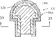
Referring now to Figure 36, be illustrated as the plan view from above of goods 62, goods 62 comprise electric insulation part 14k and the 12k of DER portion.Figure 37 is a cutaway view of taking from Figure 36 center line 37-37 perspective view basically, shows that goods 62 are mushroom-shaped.DER material 12k is bar shaped, extends to the side of mushroom-shaped goods 62 stems 60 always, gets back to the opposite side of goods 62 then by head 64.Goods 62 are convenient to known double injection mould pressing technology production.
Figure 38 and 39 illustrates the situation of goods after the additional treatment step of electroplating DER material 12k of Figure 36 and 37.The metal_based material 16k of electro-deposition extends through always and gets back to the opposite side of mushroom-shaped goods, now these goods is designated as 66, to represent this additional treatment step.Figure 39 is the cutaway view of the goods 66 of Figure 38 center line 39-39 perspective view.Those skilled in the art just understand at once, with the high conductive trace shown in conventional photomask and the extremely difficult production Figure 38 and 39 of etching technique, and in fact can't produce more complicated three-dimensional conductive trace.
The embodiment of Figure 36~39 shows material 14k and makes the DER material 12k solid insulation supporter of (with follow-up electro-deposition 16k), but hollow-core construction is more favourable sometimes, and is good especially in the Antenna Design of air being regarded as medium.
Use content of the present invention to be easy to the production hollow-core construction.The hollow-core construction that contains selective metal sill pattern is described below in conjunction with Figure 40~50." mushroom-shaped " form will be used in conjunction with Figure 40~50.
Referring now to Figure 40, illustrate common structure 68 with vertical plane among the figure at field of plastics processing middle finger parison.Parison is a hollow-core construction, and the tubular section is arranged usually, comprises the polymeric material of fusion or fritting.Parison production generally is pressed through finishing die with thermoplastic.Figure 41 is that parison shown in Figure 40 is taken from Figure 40 finishing die basically.Figure 41 is the cutaway view that parison shown in Figure 40 is taken from Figure 40 center line 41-41 perspective view basically.Make up Figure 40 and 41 as can be seen, parison 68 comprises that space 70 common great majority contain air around the hollow pipe 66 of the insulating resin 141 of gaseous space 70.The bar 67 of electroconductive resin 121 is added to hollow pipe 66 relative both sides.It will be apparent to one skilled in the art that the synchronous extruding during utilization forms parison 68, be easy to apply bar 67.Will know below, select for use DER especially favourable as material 121 to bar 67.
Figure 42 and 43 illustrates this structure after the additional treatment step.The method of producing the goods of Figure 42 and 43 is the opposite ends that earlier blow molding die two " partly " (not shown) lumped together the pinch off parison, the residue hollow space between Compressed Gas (being generally air) the injection pinch-off point, force the fusing plastic parison to prop up mould inner wall then.Repair excess stock again, obtain Figure 42 and 43 goods of implementing.
In Figure 42 and 43 embodiment, move to the left and right during mould open/close, in Figure 42, be shown MPL (mould closing line), as 72 indications of Figure 42 and 43, between the electroconductive resin bar 67 of portion about the blown-moulding goods, causing separation like this.This separates as following formation.When at first mould closes parison, earlier the interior insulating material 141 of tubular parison 68 relative both sides is clipped together, prevent to form material 121 contacts of bar 67 at parison 68 opposite sides.After blowing and repairing excess stock, just between the bar 67 that is oppositely arranged, keep gap 72.
Figure 44 is the additional cutaway view that is similar to Figure 43 behind the treatment step of selecting for use.In Figure 44, the metal_based material 161 of electro-deposition has been deposited on the electroconductive resin 121, forms the high conductive material bar that is oppositely arranged on the hollow insulation three-dimensional structure that material 141 limits.In other embodiment of the present invention, select for use DER generally to help the electro-deposition step to material 121, although this is not the absolute requirement of producing hollow conductive pattern structure shown in Figure 40~44.
Sometimes wishing or must making conductive pattern pass through extrusion blow pressing closing line has continuity.Set up this successional method and structure below in conjunction with Figure 45~50 descriptions.
Figure 45 is the vertical plane graph of parison, and parison comprises electrical insulating material 14m and electroconductive resin 1 2m.Figure 46 is a cutaway view of taking from Figure 45 center line 46-46 perspective view basically.The parisons of implementing with Figure 40 and 41 contrast, and Figure 45 and 46 electric conducting material 12m extend through the annular wall of illustrated cylindricality parison 73.Figure 45 and 46 parison structure can realize with mature technique, as be used for producing the technology that is attached to the transparent liquid level indication " observation bar " on liquid detergent and the oil bottle usually.
When on the parison that blow molding die is incorporated into Figure 45 and 46 along the MPL direction, just the relative material at opposite sides 12m of parison is picked up.Compressed Gas is blown into clamping parison cavity, makes the resin expansion prop up mould inner surface.After repairing excess stock, obtain Figure 47 and the 48 patterning hollow components of implementing 74.Figure 47 and 48 continues with mushroom-shaped the present invention to be described, but this shape obviously is not that enforcement is essential to the invention.From Figure 47 and 48 as seen, material strips 12m extends through the mould closing line continuously, and insulating material 14m makes hollow mushroom-shaped goods.
Figure 49 and 50 implements goods 76 with the goods 74 of Figure 47 and 48 additional after selecting treatment step for use.Figure 49 is the vertical cutaway view that is similar to Figure 48, and Figure 50 is a cutaway view of taking from Figure 49 center line 50-50 perspective view basically.In Figure 49 and 50, high-conductive metal sill 16m has been electro-deposited on the electric conducting material 12m surface.Electro-deposition 16m extends to goods 76 1 sides continuously, by its top again down to opposite side.
Referring now to Figure 51~56, be described in the structure and the method for making high conductive pattern on the hollw article inner surface.Figure 51 is the vertical plane graph of parison 78, and Figure 52 is a diagrammatic sketch of taking from Figure 51 center line 52-52 perspective view basically.From Figure 51 and 52 as seen, parison 78 comprises the cylindricality ring 80 of insulating material 14n, and the bar 82 of electroconductive resin 12n is positioned at cylinder 80 inner surfaces 84 relative both sides.The parison of this structure disposes available known extrusion technique production.The L of Figure 51 refers to the axial of cylindricality parison 78.Figure 53 is a cutaway view of taking from Figure 52 center line 53-53 perspective view basically, and the material strips 82 of L extension vertically is shown.
Figure 54 is the cutaway view of structure 81, and the parison 78 that structure 81 is implemented by additional treatments Figure 51~53 is made.The production method of the structure that Figure 54 implements is to close blow mold to clamp parison along the MPL direction of Figure 52 and 53 indications earlier, then Compressed Gas is injected the cavity that clamps parison, parison is extended to applying blow mold inner surface, repair each end of gained object again, make the opening 81 and 83 among Figure 54 embodiment.Opening 83 is shown circle, and diameter is D.
Figure 55 and 56 illustrates the situation of goods after additional treatment step of Figure 54.Now structure shown in Figure 55 and 56 is designated as 85, to reflect this additional treatments.Structure 85 comprises the high-conductive metal base electro-deposition material 16n that is positioned on the hollow-core construction opposed inner walls, and its form is the bar 86 that is oppositely arranged.
It will be apparent to one skilled in the art that the utilization auxiliary anode helps material 16n is electro-deposited on the inside bar 86 of Figure 55 and 56, and know that conventional photoetching technique is difficult to settle metal selectively on the hollw article inner surface, and is even unfeasible.
In above-mentioned hollow-core construction embodiment, the preliminary intermediate with extrusion blow molding process known in the art is manufactured comprises electroconductive resin and insulating resin.Should be appreciated that, also can adopt other manufacturing technology, as everyone knows the injection-blow molding molding process.In this technology, earlier produce " prefabrication " with the injection mould method for making, available combination the binary injection mould platen press of electroconductive resin and insulating resin produce this prefabrication.With Compressed Gas this " prefabrication " blown out the hollw article of expansion later on.Compare with the extrusion blow mechanograph, because of original injection molding " prefabrication " has splendid svelteness degree, so can expect to have made up the patterns of conductive materials definition of the insulating material relevant with the final blow molding mechanograph.
In the hollow-core construction of describing in conjunction with Figure 40~56, material 12l, 12m or 12n can consider some electroconductive resin prescriptions, if but on these hollw articles, form high conductive surface pattern and prepare the plated conductive resin, then DER is the preferable selection of material 12l, 12m or 12n.
Figure 57~60 illustrate another embodiment of the present invention.Figure 57 is the plan view from above of a certain intermediate during antenna is made, and Figure 58 is the flat sheet of the bottom view of this intermediate.Intermediate 87 is included in the patch 90 of the electroconductive resin 12o on its top surface, and top surface is supported by insulative dielectric material 14o.Goods 87 also are included in the patch 92 of the electroconductive resin 12o on its basal surface that is supported by material 140.Hole or path 88 extend to end face from the bottom surface, and short-circuit component 89 connects end face patch and bottom surface patchs 92.
Figure 59 is basically along the cutaway view of the line 59-59 of Figure 57 intercepting, and the material 12o that is molded into convex thread structure 94 is shown, and hole or path 88 axially extend to the pit 96 that is formed on goods 87 end faces by structure 94.Goods 84 are convenient to the production of quadric injection mould molding technique.
Figure 60 implements the goods after the intermediate 87 execution additional treatment step of Figure 57~59.For distinguishing this additional treatment step, the goods of Figure 60 are designated as 97.In goods 97, electroconductive resin 12o has been coated with high-conductive metal base electro-deposition 16o.Also electroplate threaded portion 94, constitutes the suitable low resistance connection structure of I/O coaxial cable outer conductor now.Hole or path 88 provide a raceway groove, can allow cable inner conductor reach the top patch 90 of antenna.96 pairs of scolders of recess form suitable storage ground, but the inner wire conductive adhesion of I/O cable or be mechanically connected to the patch at top.
As mentioned above, material 12o is optional from some electroconductive resins, but because of quick transverse electric deposit growth of its characteristic and good electro-deposition adhesiveness, the preferred DER of electroconductive resin 12o.
Referring now to Figure 61~63, be illustrated as another embodiment of two patch antennas.Figure 61 is the cutaway view that is similar to Figure 59 perspective view, and the intermediate 100 of manufacturing is shown, and it comprises top patch 102, short-circuit component 104, bottom patch 106, helicitic texture 108 and hole 110 and 112, and they all constitute with electroconductive resin 12p.In a preferred embodiment, electroconductive resin 12p is DER.Air 114 separates top plan patch 102 and base plane patch 106, or insulating material 14p is used as additional support, keeps the spacing of plane patch 102 and 106.
The goods 116 that Figure 63 implements produce by further processing Figure 61 and 62 goods of implementing 100.In aforementioned all examples, goods 116 are electro-deposited into electroconductive resin material 12p to the high-conductive metal sill and go up and make.The goods 116 of Figure 63 are different in two broad aspect with the goods 97 of Figure 60.The first, goods 116 are envisioned for air in the medium that separates top and bottom conduction patch 102 and 106; The second, the goods 116 of Figure 63 comprise inner surface (118 indications among Figure 63) metals deposited that powers on basic unit, and goods 97 do not have the Metal Substrate pattern of high conduction on material 120 inner surfaces.
When producing novel three-dimensional conductive trace and antenna, the present invention also proposes the profile extruding as valuable treatment technology.Figure 64~68 illustrate an example can use the material of profile extrusion technique, technology and structure.
Figure 64 is the plan view from above of the structure 120 of profile extrusion production, and Figure 65 is the flat sheet of the bottom view of described structure 120, and Figure 66 is a cutaway view of taking from Figure 64 center line 66-66 perspective view.With reference to Figure 64-66, illustrated extended structure 120 comprises the hollow box sections that insulating material 14q extends along length L direction among Figure 64, and the inside has formed the raceway groove 12l that extends along the L direction equally.Electroconductive resin material 12q is deposited in the raceway groove in length " Y " bar 122 (Figure 64) off and on.The bar 122 of imagination material 12q forms by extruding intermittently, printing, silk screen or other known technology.Figure 65 is illustrated on structure 120 bottom surfaces material 12q is positioned to continuous bar 124, and its width is slightly less than the width W of box like structure 120.Material forming bar 124 does not require with the bar 122 that is shaped congruent, and be used for deposit bar 122 can be different with 124 deposition technology.
Figure 67 and 68 goods of implementing are realized by additional treatments profile extruding 120, for showing this additional treatments, now these goods are designated as 130.During article of manufacture 130, earlier common continuous profile 120 is subdivided into the discrete-length that is decided to be X among Figure 67.Each goods that so makes are further handled by the high-conductive metal sill being electro-deposited on the electroconductive resin 12q surface again.For aforesaid reason, DER is an electroconductive resin 12q preferable material.
Figure 67 can constitute extremely consistent cheap microstrip antenna element with 68 goods 130.
Though described the present invention in conjunction with all preferred embodiments, should understand that under the situation that does not deviate from spirit of the present invention and scope, can comprise various corrections, substitute and content of equal value, those skilled in the art obviously will appreciate that.These are revised, substitute and content of equal value is considered to drop in the authority and scope of the present invention and following claim.
Claims (1)
1. but antenna that contains direct electroplating resin (DER).
Applications Claiming Priority (2)
| Application Number | Priority Date | Filing Date | Title |
|---|---|---|---|
| US09/818,128 | 2001-03-26 | ||
| US09/818,128 US6582887B2 (en) | 2001-03-26 | 2001-03-26 | Electrically conductive patterns, antennas and methods of manufacture |
Publications (1)
| Publication Number | Publication Date |
|---|---|
| CN1500296A true CN1500296A (en) | 2004-05-26 |
Family
ID=25224739
Family Applications (1)
| Application Number | Title | Priority Date | Filing Date |
|---|---|---|---|
| CNA028072162A Pending CN1500296A (en) | 2001-03-26 | 2002-03-25 | Electrically conductive patterns, antennas and methods of manufacture |
Country Status (6)
| Country | Link |
|---|---|
| US (2) | US6582887B2 (en) |
| EP (1) | EP1388186A4 (en) |
| JP (3) | JP2004533151A (en) |
| CN (1) | CN1500296A (en) |
| CA (1) | CA2441965A1 (en) |
| WO (1) | WO2002078122A1 (en) |
Cited By (4)
| Publication number | Priority date | Publication date | Assignee | Title |
|---|---|---|---|---|
| CN102011161A (en) * | 2010-11-05 | 2011-04-13 | 北京星汉特种印刷有限公司 | Plating equipment and plating method for electronic antenna |
| CN103372718A (en) * | 2012-04-17 | 2013-10-30 | 上海无线电设备研究所 | Manufacturing method for antenna waveguide soldering flakes |
| CN109417217A (en) * | 2016-09-15 | 2019-03-01 | Vega格里沙贝两合公司 | Antenna assembly |
| CN110565123A (en) * | 2019-08-28 | 2019-12-13 | 清华大学 | Manufacturing method and device of transferable transparent flexible breathable antenna |
Families Citing this family (66)
| Publication number | Priority date | Publication date | Assignee | Title |
|---|---|---|---|---|
| US7732243B2 (en) * | 1995-05-15 | 2010-06-08 | Daniel Luch | Substrate structures for integrated series connected photovoltaic arrays and process of manufacture of such arrays |
| US20080314433A1 (en) * | 1995-05-15 | 2008-12-25 | Daniel Luch | Substrate structures for integrated series connected photovoltaic arrays and process of manufacture of such arrays |
| US20090111206A1 (en) | 1999-03-30 | 2009-04-30 | Daniel Luch | Collector grid, electrode structures and interrconnect structures for photovoltaic arrays and methods of manufacture |
| US8076568B2 (en) * | 2006-04-13 | 2011-12-13 | Daniel Luch | Collector grid and interconnect structures for photovoltaic arrays and modules |
| US7635810B2 (en) * | 1999-03-30 | 2009-12-22 | Daniel Luch | Substrate and collector grid structures for integrated photovoltaic arrays and process of manufacture of such arrays |
| US8222513B2 (en) | 2006-04-13 | 2012-07-17 | Daniel Luch | Collector grid, electrode structures and interconnect structures for photovoltaic arrays and methods of manufacture |
| US20080011350A1 (en) * | 1999-03-30 | 2008-01-17 | Daniel Luch | Collector grid, electrode structures and interconnect structures for photovoltaic arrays and other optoelectric devices |
| US8138413B2 (en) | 2006-04-13 | 2012-03-20 | Daniel Luch | Collector grid and interconnect structures for photovoltaic arrays and modules |
| US20090107538A1 (en) * | 2007-10-29 | 2009-04-30 | Daniel Luch | Collector grid and interconnect structures for photovoltaic arrays and modules |
| US7507903B2 (en) | 1999-03-30 | 2009-03-24 | Daniel Luch | Substrate and collector grid structures for integrated series connected photovoltaic arrays and process of manufacture of such arrays |
| US8664030B2 (en) | 1999-03-30 | 2014-03-04 | Daniel Luch | Collector grid and interconnect structures for photovoltaic arrays and modules |
| US8198696B2 (en) | 2000-02-04 | 2012-06-12 | Daniel Luch | Substrate structures for integrated series connected photovoltaic arrays and process of manufacture of such arrays |
| US7898053B2 (en) | 2000-02-04 | 2011-03-01 | Daniel Luch | Substrate structures for integrated series connected photovoltaic arrays and process of manufacture of such arrays |
| US7898054B2 (en) | 2000-02-04 | 2011-03-01 | Daniel Luch | Substrate structures for integrated series connected photovoltaic arrays and process of manufacture of such arrays |
| US6697248B1 (en) * | 2001-02-06 | 2004-02-24 | Daniel Luch | Electromagnetic interference shields and methods of manufacture |
| US20040217472A1 (en) * | 2001-02-16 | 2004-11-04 | Integral Technologies, Inc. | Low cost chip carrier with integrated antenna, heat sink, or EMI shielding functions manufactured from conductive loaded resin-based materials |
| US6582887B2 (en) * | 2001-03-26 | 2003-06-24 | Daniel Luch | Electrically conductive patterns, antennas and methods of manufacture |
| US7452656B2 (en) | 2001-03-26 | 2008-11-18 | Ertek Inc. | Electrically conductive patterns, antennas and methods of manufacture |
| US7394425B2 (en) * | 2001-03-26 | 2008-07-01 | Daniel Luch | Electrically conductive patterns, antennas and methods of manufacture |
| US7564409B2 (en) * | 2001-03-26 | 2009-07-21 | Ertek Inc. | Antennas and electrical connections of electrical devices |
| US6894615B2 (en) * | 2001-10-09 | 2005-05-17 | 3M Innovative Properties Company | Article with retroreflective and radio frequency-responsive features |
| US6758405B2 (en) * | 2001-12-19 | 2004-07-06 | 3M Innovative Properties Company | Article with retroreflective and radio frequency-responsive features |
| JP3924512B2 (en) * | 2002-06-27 | 2007-06-06 | 株式会社東海理化電機製作所 | Chip multi-axis antenna |
| US6867983B2 (en) * | 2002-08-07 | 2005-03-15 | Avery Dennison Corporation | Radio frequency identification device and method |
| US7184800B2 (en) * | 2002-10-15 | 2007-02-27 | Kyocera Wireless Corp. | Printed stubby unbalanced dipole antenna |
| FR2847761B1 (en) * | 2002-11-27 | 2005-02-04 | Framatome Connectors Int | METALLIZING DEVICE FOR PRINTED FORMS HAVING ELECTRICALLY CONDUCTIVE SLIDES AND METHOD FOR METALLIZING THE SAME |
| US20040200061A1 (en) * | 2003-04-11 | 2004-10-14 | Coleman James P. | Conductive pattern and method of making |
| US7930815B2 (en) * | 2003-04-11 | 2011-04-26 | Avery Dennison Corporation | Conductive pattern and method of making |
| WO2004094763A2 (en) * | 2003-04-16 | 2004-11-04 | Integral Technologies, Inc. | Low cost inductor devices manufactured from conductive loaded resin-based materials |
| WO2005022556A2 (en) * | 2003-09-02 | 2005-03-10 | Integral Technologies, Inc. | Very low resistance electrical interfaces to conductive loaded resin-based materials |
| US20080272885A1 (en) * | 2004-01-22 | 2008-11-06 | Mikoh Corporation | Modular Radio Frequency Identification Tagging Method |
| US20100193367A1 (en) * | 2004-02-11 | 2010-08-05 | Daniel Luch | Methods and structures for the production of electrically treated items and electrical connections |
| US20050176270A1 (en) * | 2004-02-11 | 2005-08-11 | Daniel Luch | Methods and structures for the production of electrically treated items and electrical connections |
| US7755484B2 (en) | 2004-02-12 | 2010-07-13 | Avery Dennison Corporation | RFID tag and method of manufacturing the same |
| US8529341B2 (en) | 2004-07-27 | 2013-09-10 | Igt | Optically sensitive display for a gaming apparatus |
| US20100026590A1 (en) * | 2004-07-28 | 2010-02-04 | Kuo-Ching Chiang | Thin film multi-band antenna |
| DE102005038392B4 (en) * | 2005-08-09 | 2008-07-10 | Atotech Deutschland Gmbh | Method for producing pattern-forming copper structures on a carrier substrate |
| US20070040686A1 (en) * | 2005-08-16 | 2007-02-22 | X-Cyte, Inc., A California Corporation | RFID inlays and methods of their manufacture |
| US20070040688A1 (en) * | 2005-08-16 | 2007-02-22 | X-Cyte, Inc., A California Corporation | RFID inlays and methods of their manufacture |
| US7388542B2 (en) * | 2005-11-10 | 2008-06-17 | Rcd Technology, Inc. | Method for an element using two resist layers |
| US9236512B2 (en) | 2006-04-13 | 2016-01-12 | Daniel Luch | Collector grid and interconnect structures for photovoltaic arrays and modules |
| US9865758B2 (en) | 2006-04-13 | 2018-01-09 | Daniel Luch | Collector grid and interconnect structures for photovoltaic arrays and modules |
| US8884155B2 (en) | 2006-04-13 | 2014-11-11 | Daniel Luch | Collector grid and interconnect structures for photovoltaic arrays and modules |
| US8729385B2 (en) | 2006-04-13 | 2014-05-20 | Daniel Luch | Collector grid and interconnect structures for photovoltaic arrays and modules |
| US9006563B2 (en) | 2006-04-13 | 2015-04-14 | Solannex, Inc. | Collector grid and interconnect structures for photovoltaic arrays and modules |
| US8822810B2 (en) | 2006-04-13 | 2014-09-02 | Daniel Luch | Collector grid and interconnect structures for photovoltaic arrays and modules |
| US7836588B2 (en) | 2006-07-06 | 2010-11-23 | Ideon Llc | Method for fabricating an electronic device |
| US7605092B2 (en) * | 2007-06-29 | 2009-10-20 | Silicon Storage Technology, Inc. | Passive elements, articles, packages, semiconductor composites, and methods of manufacturing same |
| US7973722B1 (en) | 2007-08-28 | 2011-07-05 | Apple Inc. | Electronic device with conductive housing and near field antenna |
| WO2009109652A1 (en) * | 2008-03-06 | 2009-09-11 | Ceramtec Ag | Metallized coil bodies (inductor) having high q-value |
| US20090229108A1 (en) * | 2008-03-17 | 2009-09-17 | Ethertronics, Inc. | Methods for forming antennas using thermoforming |
| US7981789B2 (en) | 2008-11-14 | 2011-07-19 | Infineon Technologies Ag | Feature patterning methods and structures thereof |
| US9008589B2 (en) | 2010-01-27 | 2015-04-14 | Broadcom Corporation | Wireless bus for intra-chip and inter-chip communication, including wireless-enabled component (WEC) embodiments |
| FR2969398B1 (en) | 2010-12-20 | 2013-01-11 | St Microelectronics Sa | INTEGRATED EMITTER-RECEIVER IN MILLIMETER WAVES |
| JP6314376B2 (en) * | 2013-07-01 | 2018-04-25 | 株式会社リコー | Method for manufacturing three-dimensional structure having conductive pattern and three-dimensional structure |
| FR3019689A1 (en) * | 2014-04-02 | 2015-10-09 | Alciom | METHOD FOR MANUFACTURING TRI-DIMENSIONAL ANTENNA BY RAPID PROTOTYPING |
| US10016306B2 (en) | 2014-09-11 | 2018-07-10 | 3M Innovative Properties Company | Hearing device containing hidden FM-receiver antenna |
| TWI555450B (en) * | 2015-08-14 | 2016-10-21 | 廣州光寶移動電子部件有限公司 | Method for manufacturing conductive patterns and apparatus thereof |
| JP6069446B1 (en) * | 2015-09-28 | 2017-02-01 | 日本写真印刷株式会社 | Method for producing molded product with conductive circuit and preform with conductive circuit |
| JP7083226B2 (en) | 2016-06-10 | 2022-06-10 | 任天堂株式会社 | Game controller |
| JP6782567B2 (en) * | 2016-06-10 | 2020-11-11 | 任天堂株式会社 | Game controller |
| JP6893763B2 (en) * | 2016-06-10 | 2021-06-23 | 任天堂株式会社 | Game controller |
| EP3254739B1 (en) | 2016-06-10 | 2020-03-25 | Nintendo Co., Ltd. | Game controller |
| EP3272402B1 (en) | 2016-06-10 | 2019-02-27 | Nintendo Co., Ltd. | Game controller |
| ES2772938A1 (en) * | 2018-12-21 | 2020-07-08 | Srg Global Liria S L | SELECTIVE CHROME WITH LEVEL INTERFACE (Machine-translation by Google Translate, not legally binding) |
| TWI785774B (en) * | 2021-09-02 | 2022-12-01 | 友達光電股份有限公司 | Method of fabricating backplane |
Family Cites Families (85)
| Publication number | Priority date | Publication date | Assignee | Title |
|---|---|---|---|---|
| US3523875A (en) | 1967-03-15 | 1970-08-11 | Hooker Chemical Corp | Process for metal coating substrate pretreated with alkali metal sulfide and resultant product |
| US3619382A (en) | 1970-01-27 | 1971-11-09 | Gen Electric | Process of reducing metal compounds to metal in a matrix |
| US3682786A (en) | 1970-02-18 | 1972-08-08 | Macdermid Inc | Method of treating plastic substrates and process for plating thereon |
| US3865699A (en) | 1973-10-23 | 1975-02-11 | Int Nickel Co | Electrodeposition on non-conductive surfaces |
| US4009093A (en) | 1973-10-23 | 1977-02-22 | The International Nickel Company, Inc. | Platable polymeric composition |
| US4038042A (en) | 1975-12-18 | 1977-07-26 | E. I. Du Pont De Nemours And Company | Electroplating of polypropylene compositions |
| US4101385A (en) | 1977-03-21 | 1978-07-18 | International Nickel Company | Process for making a metal plastic structure |
| JPS5415162A (en) * | 1977-07-07 | 1979-02-03 | Victor Company Of Japan | Method of making microosize flat coil |
| US4158612A (en) | 1977-12-27 | 1979-06-19 | The International Nickel Company, Inc. | Polymeric mandrel for electroforming and method of electroforming |
| JPS5514804A (en) * | 1978-07-13 | 1980-02-01 | Toyo Terumii Kk | Method of applying partial plating to rubber or plastic |
| US4195117A (en) | 1979-03-09 | 1980-03-25 | The International Nickel Company, Inc. | Process for electroplating directly plateable plastic with nickel-iron alloy strike and article thereof |
| US4191617A (en) | 1979-03-30 | 1980-03-04 | The International Nickel Company, Inc. | Process for electroplating directly plateable plastic with cobalt alloy strike and article thereof |
| US4278510A (en) | 1980-03-31 | 1981-07-14 | Gulf Oil Corporation | Platable propylene polymer compositions |
| US4429020A (en) | 1980-05-22 | 1984-01-31 | Daniel Luch | Metal-polymer composite and method of making said composite |
| JPS5716041A (en) | 1980-05-23 | 1982-01-27 | Kureha Chem Ind Co Ltd | Electrically conductive molding resin composite material |
| JPS57137334A (en) | 1981-02-20 | 1982-08-24 | Mitsui Toatsu Chem Inc | Electrically-conductive resin composition |
| JPS57168929A (en) | 1981-04-13 | 1982-10-18 | Mitsui Toatsu Chem Inc | Improved electroconductive resin composition |
| US4603092A (en) | 1981-07-01 | 1986-07-29 | Daniel Luch | Metal-polymer composite |
| JPS62142846U (en) * | 1986-02-28 | 1987-09-09 | ||
| US4835541A (en) | 1986-12-29 | 1989-05-30 | Ball Corporation | Near-isotropic low-profile microstrip radiator especially suited for use as a mobile vehicle antenna |
| US4862184A (en) | 1987-02-06 | 1989-08-29 | George Ploussios | Method and construction of helical antenna |
| JPS6451691A (en) * | 1987-08-22 | 1989-02-27 | Matsushita Electric Works Ltd | Manufacture of printed wiring board |
| US4996391A (en) | 1988-09-30 | 1991-02-26 | Siemens Aktiengesellschaft | Printed circuit board having an injection molded substrate |
| EP0361195B1 (en) | 1988-09-30 | 1993-03-17 | Siemens Aktiengesellschaft | Printed circuit board with moulded substrate |
| US4985116A (en) | 1990-02-23 | 1991-01-15 | Mint-Pac Technologies, Inc. | Three dimensional plating or etching process and masks therefor |
| FR2673041A1 (en) | 1991-02-19 | 1992-08-21 | Gemplus Card Int | METHOD FOR MANUFACTURING INTEGRATED CIRCUIT MICROMODULES AND CORRESPONDING MICROMODULE. |
| US5206657A (en) | 1991-10-07 | 1993-04-27 | Echelon Corporation | Printed circuit radio frequency antenna |
| US5355142A (en) | 1991-10-15 | 1994-10-11 | Ball Corporation | Microstrip antenna structure suitable for use in mobile radio communications and method for making same |
| JPH0685139A (en) * | 1992-09-02 | 1994-03-25 | Toppan Printing Co Ltd | Lead frame and semiconductor device using same |
| US5567296A (en) | 1993-01-19 | 1996-10-22 | Luch; Daniel | Process for producing vehicular fuel tanks |
| US5444453A (en) | 1993-02-02 | 1995-08-22 | Ball Corporation | Microstrip antenna structure having an air gap and method of constructing same |
| AU668309B2 (en) | 1993-05-03 | 1996-04-26 | Motorola, Inc. | Antenna for an electronic apparatus |
| AU7372594A (en) | 1993-08-09 | 1995-02-28 | Motorola, Inc. | Printed circuit dipole antenna |
| BR9405603A (en) | 1993-09-20 | 1999-09-08 | Motorola Inc | Installation of antenna adapted for wireless communication device |
| JPH07142256A (en) * | 1993-11-19 | 1995-06-02 | Yokogawa Electric Corp | Stacked printed coil and its manufacture |
| DE4431605C2 (en) | 1994-09-05 | 1998-06-04 | Siemens Ag | Method for producing a chip card module for contactless chip cards |
| DE4431603A1 (en) | 1994-09-05 | 1996-03-07 | Siemens Ag | Antenna coil |
| US5596797A (en) | 1995-04-03 | 1997-01-28 | D & M Plastics Corporation | Method and apparatus for making a molded cellular antenna coil |
| US5735966A (en) | 1995-05-15 | 1998-04-07 | Luch; Daniel | Substrate structures for integrated series connected photovoltaic arrays and process of manufacture of such arrays |
| US5547516A (en) | 1995-05-15 | 1996-08-20 | Luch; Daniel | Substrate structures for integrated series connected photovoltaic arrays and process of manufacture of such arrays |
| US6459032B1 (en) | 1995-05-15 | 2002-10-01 | Daniel Luch | Substrate structures for integrated series connected photovoltaic arrays and process of manufacture of such arrays |
| CA2176625C (en) | 1995-05-19 | 2008-07-15 | Donald Harold Fergusen | Radio frequency identification tag |
| US5709832A (en) | 1995-06-02 | 1998-01-20 | Ericsson Inc. | Method of manufacturing a printed antenna |
| US5900841A (en) | 1995-11-30 | 1999-05-04 | Nihon Plast Co., Ltd | Antenna device having an antenna proper and a plastic plate attached to the antenna proper for connecting the antenna to an inside wall of a vehicle |
| US5754110A (en) * | 1996-03-07 | 1998-05-19 | Checkpoint Systems, Inc. | Security tag and manufacturing method |
| US5786626A (en) * | 1996-03-25 | 1998-07-28 | Ibm Corporation | Thin radio frequency transponder with leadframe antenna structure |
| FR2747812B1 (en) * | 1996-04-23 | 1998-05-22 | Solaic Sa | CONTACTLESS INTEGRATED CIRCUIT CARD WITH CONDUCTIVE POLYMER ANTENNA |
| JPH09294013A (en) | 1996-04-26 | 1997-11-11 | Matsushita Electric Ind Co Ltd | Antenna system |
| JPH09307329A (en) * | 1996-05-14 | 1997-11-28 | Casio Comput Co Ltd | Antenna, its manufacture and electronic device or electric watch provided with the antenna |
| US6027027A (en) | 1996-05-31 | 2000-02-22 | Lucent Technologies Inc. | Luggage tag assembly |
| US5911454A (en) | 1996-07-23 | 1999-06-15 | Trimble Navigation Limited | Microstrip manufacturing method |
| JPH10117055A (en) * | 1996-10-15 | 1998-05-06 | Shin Etsu Polymer Co Ltd | Manufacture of flexible printed circuit board |
| JPH10150259A (en) * | 1996-11-20 | 1998-06-02 | Matsushita Electric Works Ltd | Printed-wiring board with component and its manufacture |
| US6052889A (en) | 1996-11-21 | 2000-04-25 | Raytheon Company | Radio frequency antenna and its fabrication |
| US5898215A (en) | 1996-12-16 | 1999-04-27 | Motorola, Inc. | Microelectronic assembly with connection to a buried electrical element, and method for forming same |
| FI112723B (en) | 1997-03-27 | 2003-12-31 | Nokia Corp | Antenna for wireless telephones |
| US6147660A (en) | 1997-06-03 | 2000-11-14 | Galtronics Ltd. | Molded antenna |
| US6049463A (en) | 1997-07-25 | 2000-04-11 | Motorola, Inc. | Microelectronic assembly including an antenna element embedded within a polymeric card, and method for forming same |
| US6052088A (en) | 1997-08-26 | 2000-04-18 | Centurion International, Inc. | Multi-band antenna |
| US6081243A (en) | 1997-09-09 | 2000-06-27 | Micron Technology, Inc. | Methods of forming conductive lines, methods of forming antennas, methods of forming wireless communication devices, conductive lines, antennas, and wireless communications devices |
| ES2199705T1 (en) | 1997-09-11 | 2004-03-01 | Prec Dynamics Corp | IDENTIFICATION TRANSPONDER WITH INTEGRATED CIRCUIT CONSISTING OF ORGANIC MATERIALS. |
| EP0903805B1 (en) * | 1997-09-19 | 2003-08-06 | Peter Vernon | Planar antenna device |
| US6168855B1 (en) | 1997-12-01 | 2001-01-02 | Polyeitan Composites Ltd. | Polyolefin composites for printed circuit board and antenna base material |
| US6184833B1 (en) | 1998-02-23 | 2001-02-06 | Qualcomm, Inc. | Dual strip antenna |
| JPH11261325A (en) | 1998-03-10 | 1999-09-24 | Shiro Sugimura | Coil element and its manufacture |
| US5995052A (en) | 1998-05-15 | 1999-11-30 | Ericsson Inc. | Flip open antenna for a communication device |
| US6107920A (en) | 1998-06-09 | 2000-08-22 | Motorola, Inc. | Radio frequency identification tag having an article integrated antenna |
| US6161761A (en) | 1998-07-09 | 2000-12-19 | Motorola, Inc. | Card assembly having a loop antenna formed of a bare conductor and method for manufacturing the card assembly |
| US6075489A (en) | 1998-09-09 | 2000-06-13 | Centurion Intl., Inc. | Collapsible antenna |
| AU5809099A (en) * | 1998-09-11 | 2000-04-03 | Motorola, Inc. | Radio frequency identification tag apparatus and related method |
| JP2000113147A (en) * | 1998-10-08 | 2000-04-21 | Hitachi Chem Co Ltd | Ic card and its manufacture |
| US6049314A (en) | 1998-11-17 | 2000-04-11 | Xertex Technologies, Inc. | Wide band antenna having unitary radiator/ground plane |
| US6163260A (en) | 1998-12-10 | 2000-12-19 | Intermec Ip Corp. | Linerless label tracking system |
| US6343208B1 (en) | 1998-12-16 | 2002-01-29 | Telefonaktiebolaget Lm Ericsson (Publ) | Printed multi-band patch antenna |
| EP1020947A3 (en) * | 1998-12-22 | 2000-10-04 | Nokia Mobile Phones Ltd. | Method for manufacturing an antenna body for a phone and phone or handset having an internal antenna |
| US6157344A (en) | 1999-02-05 | 2000-12-05 | Xertex Technologies, Inc. | Flat panel antenna |
| JP2000265086A (en) * | 1999-03-11 | 2000-09-26 | Mikuni Color Ltd | Conductive coating composition and method for imparting conductivity using the same |
| US6239352B1 (en) | 1999-03-30 | 2001-05-29 | Daniel Luch | Substrate and collector grid structures for electrically interconnecting photovoltaic arrays and process of manufacture of such arrays |
| US6255999B1 (en) | 1999-04-28 | 2001-07-03 | The Whitaker Corporation | Antenna element having a zig zag pattern |
| US6137452A (en) | 1999-05-03 | 2000-10-24 | Centurion International, Inc. | Double shot antenna |
| US6259369B1 (en) | 1999-09-30 | 2001-07-10 | Moore North America, Inc. | Low cost long distance RFID reading |
| US6271793B1 (en) | 1999-11-05 | 2001-08-07 | International Business Machines Corporation | Radio frequency (RF) transponder (Tag) with composite antenna |
| US6331838B1 (en) | 2000-07-19 | 2001-12-18 | Delphi Technologies, Inc. | Flexible vehicle antenna |
| US6697248B1 (en) * | 2001-02-06 | 2004-02-24 | Daniel Luch | Electromagnetic interference shields and methods of manufacture |
| US6582887B2 (en) * | 2001-03-26 | 2003-06-24 | Daniel Luch | Electrically conductive patterns, antennas and methods of manufacture |
-
2001
- 2001-03-26 US US09/818,128 patent/US6582887B2/en not_active Expired - Fee Related
-
2002
- 2002-03-25 EP EP02753858A patent/EP1388186A4/en not_active Withdrawn
- 2002-03-25 CA CA002441965A patent/CA2441965A1/en not_active Abandoned
- 2002-03-25 US US10/472,875 patent/US20040090380A1/en not_active Abandoned
- 2002-03-25 JP JP2002576050A patent/JP2004533151A/en active Pending
- 2002-03-25 CN CNA028072162A patent/CN1500296A/en active Pending
- 2002-03-25 WO PCT/US2002/009408 patent/WO2002078122A1/en active Application Filing
-
2006
- 2006-12-26 JP JP2006350173A patent/JP2007129759A/en active Pending
-
2007
- 2007-04-11 JP JP2007103996A patent/JP2007282247A/en active Pending
Cited By (5)
| Publication number | Priority date | Publication date | Assignee | Title |
|---|---|---|---|---|
| CN102011161A (en) * | 2010-11-05 | 2011-04-13 | 北京星汉特种印刷有限公司 | Plating equipment and plating method for electronic antenna |
| CN103372718A (en) * | 2012-04-17 | 2013-10-30 | 上海无线电设备研究所 | Manufacturing method for antenna waveguide soldering flakes |
| CN109417217A (en) * | 2016-09-15 | 2019-03-01 | Vega格里沙贝两合公司 | Antenna assembly |
| CN110565123A (en) * | 2019-08-28 | 2019-12-13 | 清华大学 | Manufacturing method and device of transferable transparent flexible breathable antenna |
| CN110565123B (en) * | 2019-08-28 | 2021-06-08 | 清华大学 | Manufacturing method and device of transferable transparent flexible breathable antenna |
Also Published As
| Publication number | Publication date |
|---|---|
| WO2002078122A1 (en) | 2002-10-03 |
| JP2007282247A (en) | 2007-10-25 |
| EP1388186A1 (en) | 2004-02-11 |
| CA2441965A1 (en) | 2002-10-03 |
| JP2004533151A (en) | 2004-10-28 |
| US20040090380A1 (en) | 2004-05-13 |
| US20020135519A1 (en) | 2002-09-26 |
| JP2007129759A (en) | 2007-05-24 |
| US6582887B2 (en) | 2003-06-24 |
| EP1388186A4 (en) | 2005-08-17 |
Similar Documents
| Publication | Publication Date | Title |
|---|---|---|
| CN1500296A (en) | Electrically conductive patterns, antennas and methods of manufacture | |
| US7394425B2 (en) | Electrically conductive patterns, antennas and methods of manufacture | |
| US20070169336A1 (en) | Electrically conductive patterns, antennas and methods of manufacture | |
| US7564409B2 (en) | Antennas and electrical connections of electrical devices | |
| CN102376416B (en) | Coil device | |
| CN1258777C (en) | High density inductor and method for producing same | |
| CN1260746C (en) | Thin film type common mode choke and its producing method | |
| CN107535080B (en) | Electronic circuit module | |
| CN1198300C (en) | Manufacture method and device for solid electrolytic condenser | |
| CN1918677A (en) | Solid electrolytic capacitor | |
| JP2003519442A (en) | Method, equipment and apparatus for manufacturing electrical connection elements, electrical connection elements and semi-finished products | |
| US7452656B2 (en) | Electrically conductive patterns, antennas and methods of manufacture | |
| US20100156723A1 (en) | Electrically conductive patterns, antennas and methods of manufacture | |
| CN1499548A (en) | Solid electrolytic condenser and its mfg. method | |
| CN104756208A (en) | Production method for coil element, coil element assembly, and coil component | |
| US20210005378A1 (en) | Magnetic element, manufacturing method of magnetic element, and power module | |
| CN1256007C (en) | Laminated ceramic electronic component and manufacturing method thereof | |
| EP4216244A1 (en) | Magnetic element and power module | |
| CN106332461B (en) | Circuit board and preparation method thereof | |
| CN101909399A (en) | Circuit board structure and manufacture method thereof | |
| CN1619724A (en) | Magnetic device | |
| CN206376020U (en) | A kind of electroplate jig | |
| US8590140B2 (en) | Method for manufacturing alloy resistor | |
| CN106332437A (en) | Electroplating method | |
| CN104768319A (en) | Printed circuit board and manufacturing method thereof |
Legal Events
| Date | Code | Title | Description |
|---|---|---|---|
| C06 | Publication | ||
| PB01 | Publication | ||
| C10 | Entry into substantive examination | ||
| SE01 | Entry into force of request for substantive examination | ||
| C02 | Deemed withdrawal of patent application after publication (patent law 2001) | ||
| WD01 | Invention patent application deemed withdrawn after publication |
Open date: 20040526 |