CN1355903A - Interface for coupling bus node to bus line of bus system - Google Patents
Interface for coupling bus node to bus line of bus system Download PDFInfo
- Publication number
- CN1355903A CN1355903A CN00808742A CN00808742A CN1355903A CN 1355903 A CN1355903 A CN 1355903A CN 00808742 A CN00808742 A CN 00808742A CN 00808742 A CN00808742 A CN 00808742A CN 1355903 A CN1355903 A CN 1355903A
- Authority
- CN
- China
- Prior art keywords
- bus
- voltage
- interface
- user
- vext
- Prior art date
- Legal status (The legal status is an assumption and is not a legal conclusion. Google has not performed a legal analysis and makes no representation as to the accuracy of the status listed.)
- Pending
Links
Images

Classifications
-
- H—ELECTRICITY
- H04—ELECTRIC COMMUNICATION TECHNIQUE
- H04L—TRANSMISSION OF DIGITAL INFORMATION, e.g. TELEGRAPHIC COMMUNICATION
- H04L12/00—Data switching networks
- H04L12/28—Data switching networks characterised by path configuration, e.g. LAN [Local Area Networks] or WAN [Wide Area Networks]
- H04L12/40—Bus networks
- H04L12/40006—Architecture of a communication node
- H04L12/40039—Details regarding the setting of the power status of a node according to activity on the bus
-
- G—PHYSICS
- G06—COMPUTING; CALCULATING OR COUNTING
- G06F—ELECTRIC DIGITAL DATA PROCESSING
- G06F13/00—Interconnection of, or transfer of information or other signals between, memories, input/output devices or central processing units
- G06F13/38—Information transfer, e.g. on bus
- G06F13/40—Bus structure
- G06F13/4063—Device-to-bus coupling
- G06F13/4068—Electrical coupling
-
- H—ELECTRICITY
- H03—ELECTRONIC CIRCUITRY
- H03K—PULSE TECHNIQUE
- H03K17/00—Electronic switching or gating, i.e. not by contact-making and –breaking
- H03K17/22—Modifications for ensuring a predetermined initial state when the supply voltage has been applied
-
- H—ELECTRICITY
- H03—ELECTRONIC CIRCUITRY
- H03K—PULSE TECHNIQUE
- H03K19/00—Logic circuits, i.e. having at least two inputs acting on one output; Inverting circuits
- H03K19/003—Modifications for increasing the reliability for protection
-
- H—ELECTRICITY
- H03—ELECTRONIC CIRCUITRY
- H03K—PULSE TECHNIQUE
- H03K19/00—Logic circuits, i.e. having at least two inputs acting on one output; Inverting circuits
- H03K19/0175—Coupling arrangements; Interface arrangements
-
- H—ELECTRICITY
- H04—ELECTRIC COMMUNICATION TECHNIQUE
- H04L—TRANSMISSION OF DIGITAL INFORMATION, e.g. TELEGRAPHIC COMMUNICATION
- H04L12/00—Data switching networks
- H04L12/02—Details
- H04L12/10—Current supply arrangements
-
- H—ELECTRICITY
- H04—ELECTRIC COMMUNICATION TECHNIQUE
- H04L—TRANSMISSION OF DIGITAL INFORMATION, e.g. TELEGRAPHIC COMMUNICATION
- H04L12/00—Data switching networks
- H04L12/28—Data switching networks characterised by path configuration, e.g. LAN [Local Area Networks] or WAN [Wide Area Networks]
- H04L12/40—Bus networks
Landscapes
- Engineering & Computer Science (AREA)
- Computer Hardware Design (AREA)
- General Engineering & Computer Science (AREA)
- Computer Networks & Wireless Communication (AREA)
- Signal Processing (AREA)
- Physics & Mathematics (AREA)
- Mathematical Physics (AREA)
- Theoretical Computer Science (AREA)
- Computing Systems (AREA)
- General Physics & Mathematics (AREA)
- Small-Scale Networks (AREA)
- Interface Circuits In Exchanges (AREA)
- Cable Transmission Systems, Equalization Of Radio And Reduction Of Echo (AREA)
- Communication Control (AREA)
- Power Sources (AREA)
Abstract
The invention relates to an interface (2) for coupling a bus node (6) to the bus line of a bus system (4). According to the invention, the inventive interface comprises an input (10) for an external supply voltage (Vext) which is provided by a bus-independent voltage source (8), and comprises a monitoring circuit (30). Said monitoring circuit is provided for comparing an internal supply voltage (Vcc) derived from the bus voltage with the external supply voltage (Vext) and for generating an output control signal (R) for the bus node (6) based on the result of the comparison.
Description
The present invention relates to a kind of being used for is coupled to bus user the bus of bus system, especially is coupled to interface on the bus system EIB of the EIBA of europe installation bus association.
Described bus system EIB is a kind of dual-wire bus system, wherein, is connected to the power supply of the bus user on the bus system and the data transmission between them is to be incorporated in a lead to last through interface.In this bus system, the electric current of taking of each bus user is only limited to for example 10mA.But this limited electric current of taking not is can both satisfy all bus users under all applicable cases, so that need to give the bus user with high current requirement that a kind of external voltage is provided.This additional, with the irrelevant externally fed of bus also be favourable for the supply load that alleviates EIB.
To produce following situation for this reason,, be connected to bus user on the bus system by an outside, carry out feed with its irrelevant voltage source through this interface though be by EIB self power supply promptly such as interfaces such as TPUART-IC.
The known interface of using in EIB produces a control signal (reset signal) as bus user, have only supply voltage when bus user to reach a predetermined value and this bus user and obtained the enough time when being used for correctly starting, just utilize described control signal to discharge exchanges data.Lacking under the not enough situation of bus voltage or bus voltage, described interface will be exported a binary control signal value, such as low level (=reset effectively), utilize this control signal to guarantee not carry out exchanges data.Have only when the supply voltage of described interface with when the bus voltage that this interface is sent to bus user has reached a predetermined value, just described control signal is changed to another value, such as high level (=it is invalid to reset), realize exchanges data then.
For the bus user that utilizes external power supply to power, may enter following duty this moment, wherein, bus voltage also is not in enough height on the one hand, and provide externally fed voltage for bus user on the other hand, like this, bus user is effectively, but itself provides its work needed enough supply voltages for described interface.In this case, the launch attempt of bus user will cause a rub-out signal.
At this, the present invention based on task be to provide interface on a kind of bus that bus user is coupled to bus system, utilize it can avoid above-mentioned misoperation state.
According to the present invention, described task will utilize a kind of interface with characteristic of claim 1 to solve.Interface of the present invention includes a kind of input end and a kind of monitoring circuit, described input end be used for by with the irrelevant externally fed voltage that voltage source provided of bus, and described monitoring circuit is used to relatively the internal supply voltage and the described externally fed voltage of deriving from described bus voltage, and produces an output control signal for described bus user according to comparative result.Can guarantee to have only by this measure and when interface is in orderly duty, just discharge described bus user.
In a kind of preferred extension of the present invention, described output control signal is a binary signal, utilizes from inside that described internal supply voltage and described externally fed voltage are derived respectively and the symbol of the difference of external reference voltage is determined the value of described binary signal.This interface of the present invention especially can be used for following bus system by installing, and this bus system comprises at least one bus user, and this bus user provides externally fed voltage by a voltage source that has nothing to do with bus.
Interface of the present invention also can be used to the bus user that is coupled and powered by bus voltage.To this, only need the input end of described externally fed voltage to be shorted on the output terminal of described internal supply voltage just passable according to preferred extension of the present invention.
In order further to set forth the present invention, please refer to embodiment shown in the drawings.Wherein:
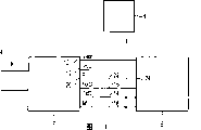
Fig. 1 shows the interface of the present invention that is connected to bus user on it with block diagram,
Fig. 2 shows the preferred extension of a kind of monitoring circuit that is used for interface of the present invention.
As shown in Figure 1, for example be connected to for the interface 2 of TPUART-IC such as for dual-wire bus system, especially be on the bus system 4 of EIB.Bus user 6 is connected on the bus system 4 by this interface 2, and this bus user 6 comprises its distinctive consumer electronic device.
By an externally fed voltage Vext being provided for described bus user 6 with the irrelevant voltage source 8 of bus.This voltage source 8 is irrelevant with bus on following meaning, and promptly supply voltage Vext of its generation and bus voltage are irrelevant, and loads load for bus system 4.
The voltage source 8 irrelevant with bus is connected on the voltage input end 10 of interface 2.Interface 2 provides an internal supply voltage Vcc who draws from the bus voltage of bus system 4 on voltage output end 12, this voltage is prescribed and is used for not having to provide power supply with the user who links to each other with the irrelevant voltage source 8 of bus to one.In this embodiment, this voltage output end 12 does not link to each other with bus user 6, because this user powers by external voltage source 8.Between bus system 4 and bus user 6, carry out the exchange of data TxD and RxD by transmitting and receiving line 14,16.Utilize ground wire 18 that interface 2 and bus user 6 are changed to identical reference potential M.
Have an output control signal R on the control output end 20 of described interface 2, it is sent on the voltage input end 24 of bus user 6 by control line 22.This output control signal R is a binary signal with two kinds of possibility state values, discharges bus user 6 by its and goes to receive and transmit data.
As shown in Figure 2, interface 2 comprises a monitoring circuit with comparer 32, utilizes this comparer to come internal supply voltage Vcc and the described externally fed voltage Vext that relatively derives from described bus voltage.Externally fed voltage Vext is connected to earth potential M by the Zener diode Z of protective resistance R1 and series connection with it.The positive input terminal of comparer 32 is connected between Zener diode Z and the protective resistance R1.
In case described externally fed voltage Vext surpasses the Zener voltage of Zener diode Z, then one and the corresponding constant external reference voltage Vref of this Zener voltage, ext can appear in the positive input terminal at comparer 32.With this external reference voltage Vref, that ext derives with supply voltage Vcc internally, through the internal reference voltage Vref that bleeder circuit R2 and R3 provide, int compares.This comparer 32 produces a binary internal control signal S on its output terminal, and this control signal depends on described external reference voltage Vref, the symbol of the difference of ext and described internal supply voltage Vcc.Described internal control signal S is given on the gate pole of MOS field effect transistor, and the drain electrode of this MOS field effect transistor is received on the described control output end 20.
When the output terminal of described comparer 32 was not controlled voltage (internal control signal S=is low), described MOS field effect transistor was in cut-off state.If the comparer 32 of being powered by external voltage source is because of lacking externally fed voltage Vext or the not enough and offhand work of this supply voltage, perhaps described internal reference voltage Vref, int is less than described external reference voltage Vref, and ext above-mentioned situation will always occur so.
Produce described output control signal R according to described internal control signal S and according to this method from externally fed voltage Vext, its value is assumed that 0 (low level) and Vext (high level) in this embodiment.Utilize suitable voltage transfer circuit, can the magnitude of voltage of high level state be adjusted to 0 and Vext between arbitrary value.
Another one MOS field effect transistor 36 in parallel on MOS field effect transistor 34, its gate pole is received on the internal module 38, this internal module produces a control voltage to be used for the gate pole of MOS field effect transistor 36 among the supply voltage Vcc internally, like this, the just alternative MOS field effect transistor 34 of this MOS field effect transistor 36 produces output control signal R.
In order to keep the functional of described interface 2 lacking under the situation of externally fed, be shorted on the voltage input end 20 at following described voltage output end 12 of this working method, this is to show with the electric bridge shown in the dot-and-dash line 40 in the accompanying drawings.
Claims (4)
1. be used for bus user (6) is coupled to interface (2) on the bus of bus system (4), have a kind of input end (10) and a kind of monitoring circuit (30), described input end is the externally fed voltage (Vext) that is used for by being provided with the irrelevant voltage source (8) of bus, and described monitoring circuit is used to relatively internal supply voltage (Vcc) and the described externally fed voltage (Vext) of deriving from described bus voltage, and produces one for described bus user (6) according to comparative result and export control signal (R).
2. interface as claimed in claim 1 (2), wherein, described output control signal (R) is a binary signal, inside and external reference voltage (Vref that utilization is derived respectively from described internal supply voltage (Vcc) and described externally fed voltage (Vext), int and Vref, the symbol of difference ext) is determined the value of described binary signal.
3. the bus system that has interface as claimed in claim 1 or 2 (2), also have a kind of and bus irrelevant, be used for voltage source (8) at least one bus user (6) power supply.
4. the bus system that has interface as claimed in claim 1 or 2 (2), wherein, when bus user (6) was powered by described internal supply voltage (Vcc), the input end of described externally fed voltage (10) was shorted on the voltage output end (12) of described internal supply voltage (Vcc).
Applications Claiming Priority (2)
| Application Number | Priority Date | Filing Date | Title |
|---|---|---|---|
| DE19926095A DE19926095A1 (en) | 1999-06-08 | 1999-06-08 | Interface for coupling a bus device to the bus line of a bus system |
| DE19926095.8 | 1999-06-08 |
Publications (1)
| Publication Number | Publication Date |
|---|---|
| CN1355903A true CN1355903A (en) | 2002-06-26 |
Family
ID=7910548
Family Applications (1)
| Application Number | Title | Priority Date | Filing Date |
|---|---|---|---|
| CN00808742A Pending CN1355903A (en) | 1999-06-08 | 2000-05-26 | Interface for coupling bus node to bus line of bus system |
Country Status (7)
| Country | Link |
|---|---|
| EP (1) | EP1192551B1 (en) |
| CN (1) | CN1355903A (en) |
| AT (1) | ATE230862T1 (en) |
| AU (1) | AU6258600A (en) |
| DE (2) | DE19926095A1 (en) |
| HK (1) | HK1047641A1 (en) |
| WO (1) | WO2000075794A1 (en) |
Cited By (2)
| Publication number | Priority date | Publication date | Assignee | Title |
|---|---|---|---|---|
| CN102783082A (en) * | 2010-03-09 | 2012-11-14 | 罗伯特·博世有限公司 | Method for feeding at least one bus subscriber |
| CN103345292A (en) * | 2013-06-28 | 2013-10-09 | 广东威创视讯科技股份有限公司 | Apparatus for protecting power supply based on the power supply of DVI interface |
Families Citing this family (4)
| Publication number | Priority date | Publication date | Assignee | Title |
|---|---|---|---|---|
| WO2002033843A1 (en) * | 2000-10-19 | 2002-04-25 | Siemens Aktiengesellschaft | Driver circuit |
| DE20315837U1 (en) * | 2003-10-15 | 2005-03-03 | Weidmüller Interface GmbH & Co. KG | Distributor for connecting electrical equipment with multiple power supply |
| DE102013013466B4 (en) * | 2013-08-14 | 2018-12-20 | Endress + Hauser Wetzer Gmbh + Co. Kg | Operating electronics for a two-wire process device |
| EP3240133B1 (en) | 2016-04-28 | 2018-12-12 | Siemens Aktiengesellschaft | Bus participants |
Family Cites Families (5)
| Publication number | Priority date | Publication date | Assignee | Title |
|---|---|---|---|---|
| JPH01193953A (en) * | 1988-01-28 | 1989-08-03 | Pfu Ltd | System for detecting abnormality of bus |
| DE19637580A1 (en) * | 1996-09-14 | 1998-03-19 | Insta Elektro Gmbh & Co Kg | Electronic data coupling component group |
| DE19639635C1 (en) * | 1996-09-26 | 1998-07-09 | Texas Instruments Deutschland | CMOS-bus driver circuit for data bus system |
| US5838073A (en) * | 1997-01-21 | 1998-11-17 | Dell Usa, L.P. | Sideband communication on the standard parallel SCSI bus |
| DE29900129U1 (en) * | 1998-11-19 | 1999-08-26 | Lingg & Janke oHG, 78315 Radolfzell | Device for coupling to a bus |
-
1999
- 1999-06-08 DE DE19926095A patent/DE19926095A1/en not_active Withdrawn
-
2000
- 2000-05-26 WO PCT/DE2000/001712 patent/WO2000075794A1/en active IP Right Grant
- 2000-05-26 AT AT00949062T patent/ATE230862T1/en active
- 2000-05-26 AU AU62586/00A patent/AU6258600A/en not_active Abandoned
- 2000-05-26 CN CN00808742A patent/CN1355903A/en active Pending
- 2000-05-26 EP EP00949062A patent/EP1192551B1/en not_active Expired - Lifetime
- 2000-05-26 DE DE50001066T patent/DE50001066D1/en not_active Expired - Lifetime
-
2002
- 2002-12-19 HK HK02109210.3A patent/HK1047641A1/en unknown
Cited By (5)
| Publication number | Priority date | Publication date | Assignee | Title |
|---|---|---|---|---|
| CN102783082A (en) * | 2010-03-09 | 2012-11-14 | 罗伯特·博世有限公司 | Method for feeding at least one bus subscriber |
| US8855216B2 (en) | 2010-03-09 | 2014-10-07 | Robert Bosch Gmbh | Method for supplying at least one bus user |
| CN102783082B (en) * | 2010-03-09 | 2015-05-20 | 罗伯特·博世有限公司 | Method for feeding at least one bus subscriber |
| CN103345292A (en) * | 2013-06-28 | 2013-10-09 | 广东威创视讯科技股份有限公司 | Apparatus for protecting power supply based on the power supply of DVI interface |
| CN103345292B (en) * | 2013-06-28 | 2015-12-23 | 广东威创视讯科技股份有限公司 | Based on the apparatus for protecting power supply that DVI interface is powered |
Also Published As
| Publication number | Publication date |
|---|---|
| HK1047641A1 (en) | 2003-02-28 |
| EP1192551A1 (en) | 2002-04-03 |
| ATE230862T1 (en) | 2003-01-15 |
| DE50001066D1 (en) | 2003-02-13 |
| AU6258600A (en) | 2000-12-28 |
| EP1192551B1 (en) | 2003-01-08 |
| DE19926095A1 (en) | 2000-12-14 |
| WO2000075794A1 (en) | 2000-12-14 |
Similar Documents
| Publication | Publication Date | Title |
|---|---|---|
| CN103380556B (en) | For Wireless Telecom Equipment electric power management circuit and use its process control system | |
| TWI754588B (en) | System for transmitting power to a remote poe subsystem by forwarding pd input voltage and manufacturing method, using method, and non-transitory program storage device readable by a computing device of the same | |
| US20200228353A1 (en) | Energy-saving power sourcing method, power sourcing equipment, and powered device | |
| CN112803563B (en) | Low-voltage starting circuit for low-inductance wireless charging system and wireless charging system | |
| CN1877949A (en) | Method of forming an in-rush limiter and structure therefor | |
| SE515882C2 (en) | Electrical power management system and radio communication device comprising such a system | |
| KR101727964B1 (en) | Device capable of compensating current thereof and memory device | |
| CN101529358B (en) | Method for reducing oscillations in system with foldback current limit when inductive load is connected | |
| CN1355903A (en) | Interface for coupling bus node to bus line of bus system | |
| CN1296593A (en) | Data carrier for contactless and contacted operation | |
| US20130221944A1 (en) | Power Supplies Responsive To Multiple Control Signal Formats | |
| CN102346529A (en) | Power supply control circuit | |
| CN107239129A (en) | The power control method and device of a kind of electronic equipment | |
| US20230046723A1 (en) | Power over Ethernet system having multiple power source devices | |
| CN216748486U (en) | Two-bus equipment capable of returning various information | |
| CN101101502A (en) | Network control device and network chip starting method | |
| CN1212392A (en) | Method for protecting CPU against damage owing to overvoltage and overcurrent | |
| CN113966025B (en) | Dimming method, dimming controller and dimming control system | |
| CN102890553A (en) | Memory and memory power supply system with same | |
| US7034604B2 (en) | Communications device powered from host apparatus | |
| CN109391277A (en) | A kind of cascade bus signal receiving circuit and control system | |
| CN115800690A (en) | Control method of driving circuit, power supply circuit and electronic equipment | |
| US20120209936A1 (en) | Communication circuit and method utilizing a single communication line | |
| CN109586363B (en) | Charging circuit | |
| CN103440008B (en) | Self-adaptive load circuit with output voltage regulation function |
Legal Events
| Date | Code | Title | Description |
|---|---|---|---|
| C06 | Publication | ||
| PB01 | Publication | ||
| C10 | Entry into substantive examination | ||
| SE01 | Entry into force of request for substantive examination | ||
| C02 | Deemed withdrawal of patent application after publication (patent law 2001) | ||
| WD01 | Invention patent application deemed withdrawn after publication | ||
| REG | Reference to a national code |
Ref country code: HK Ref legal event code: WD Ref document number: 1047641 Country of ref document: HK |