CN1324674C - Method for bonding and transferring a material to form a semiconductor device - Google Patents
Method for bonding and transferring a material to form a semiconductor device Download PDFInfo
- Publication number
- CN1324674C CN1324674C CNB028272463A CN02827246A CN1324674C CN 1324674 C CN1324674 C CN 1324674C CN B028272463 A CNB028272463 A CN B028272463A CN 02827246 A CN02827246 A CN 02827246A CN 1324674 C CN1324674 C CN 1324674C
- Authority
- CN
- China
- Prior art keywords
- substrate
- donor
- semiconductor substrate
- bonding
- transfer layer
- Prior art date
- Legal status (The legal status is an assumption and is not a legal conclusion. Google has not performed a legal analysis and makes no representation as to the accuracy of the status listed.)
- Expired - Fee Related
Links
Images


Classifications
-
- H—ELECTRICITY
- H01—ELECTRIC ELEMENTS
- H01L—SEMICONDUCTOR DEVICES NOT COVERED BY CLASS H10
- H01L21/00—Processes or apparatus adapted for the manufacture or treatment of semiconductor or solid state devices or of parts thereof
- H01L21/02—Manufacture or treatment of semiconductor devices or of parts thereof
- H01L21/04—Manufacture or treatment of semiconductor devices or of parts thereof the devices having at least one potential-jump barrier or surface barrier, e.g. PN junction, depletion layer or carrier concentration layer
- H01L21/18—Manufacture or treatment of semiconductor devices or of parts thereof the devices having at least one potential-jump barrier or surface barrier, e.g. PN junction, depletion layer or carrier concentration layer the devices having semiconductor bodies comprising elements of Group IV of the Periodic System or AIIIBV compounds with or without impurities, e.g. doping materials
- H01L21/20—Deposition of semiconductor materials on a substrate, e.g. epitaxial growth solid phase epitaxy
- H01L21/2003—Deposition of semiconductor materials on a substrate, e.g. epitaxial growth solid phase epitaxy characterised by the substrate
- H01L21/2007—Bonding of semiconductor wafers to insulating substrates or to semiconducting substrates using an intermediate insulating layer
-
- H—ELECTRICITY
- H01—ELECTRIC ELEMENTS
- H01L—SEMICONDUCTOR DEVICES NOT COVERED BY CLASS H10
- H01L21/00—Processes or apparatus adapted for the manufacture or treatment of semiconductor or solid state devices or of parts thereof
- H01L21/70—Manufacture or treatment of devices consisting of a plurality of solid state components formed in or on a common substrate or of parts thereof; Manufacture of integrated circuit devices or of parts thereof
- H01L21/71—Manufacture of specific parts of devices defined in group H01L21/70
- H01L21/76—Making of isolation regions between components
- H01L21/762—Dielectric regions, e.g. EPIC dielectric isolation, LOCOS; Trench refilling techniques, SOI technology, use of channel stoppers
- H01L21/7624—Dielectric regions, e.g. EPIC dielectric isolation, LOCOS; Trench refilling techniques, SOI technology, use of channel stoppers using semiconductor on insulator [SOI] technology
- H01L21/76251—Dielectric regions, e.g. EPIC dielectric isolation, LOCOS; Trench refilling techniques, SOI technology, use of channel stoppers using semiconductor on insulator [SOI] technology using bonding techniques
- H01L21/76254—Dielectric regions, e.g. EPIC dielectric isolation, LOCOS; Trench refilling techniques, SOI technology, use of channel stoppers using semiconductor on insulator [SOI] technology using bonding techniques with separation/delamination along an ion implanted layer, e.g. Smart-cut, Unibond
Abstract
The invention discloses a method for manufacturing a semiconductor device. A donor substrate (12) patterned to have a donor mesa (18) is bonded to a receiving substrate (20). In one embodiment, the bulk portion of the donor substrate is removed, but a transfer layer (26) remains bonded to the receiving substrate. The transfer layer is a layer of material transferred from the donor mesa. A portion of the receiving substrate may be processed to form a cavity (27, 28, or 32) for receiving a donor mesa. Alternatively, the transfer layer may be formed on a prosthetic component (46) formed on the receiving substrate, in which case the donor substrate may or may not have mesas. In a preferred embodiment, the transfer layer is used to form an optical device such as a photodetector in a semiconductor device. With the present invention, bonding can be achieved regardless of whether the surface of the receiving substrate is planar or not.
Description
Technical field
Present invention relates in general to the manufacturing of semiconductor device, more specifically, the present invention relates to a kind of technology that adopts the wafer bonding method to make semiconductor device.
Background technology
The wafer bonding method is a kind of known technology, and it is used for forming two kinds of distinct single-crystal semiconductor materials at the same device that finally makes.These two kinds of materials can be of identical composition, and perhaps also can be different materials.By way of example, two silicon wafers can be bonded to together, perhaps can be to a silicon wafer with germanium wafer or gallium wafer bonding.As a rule, the two plates that bonding is separated by a dielectric layer, and this dielectric layer is not only as electric insulation layer, also as the knitting layer that constitutes key compound.
For the occasion that will on two semiconductor wafers, all make device, wish that wherein a wafer should sufficiently approach, so that the manufacturing of device and the line that forms this device.But as carrying out technology since an enough thin wafer, the operation that then it is bonded to the acceptor wafer will be difficult to realize that reason is the structural strength deficiency of LED reverse mounting type.Making the enough thin a kind of method of bonded layer thickness is after bonding the back side of a wafer wherein to be lost deeply.But for the extremely thin situation of thickness of the obtained layer of hope body, this method may be unfavorable, and reason is to etch away a large amount of wafer materials, and the uniformity of wayward wafer rest layers thickness.Developed in the prior art and a kind of alternative technology, it can be transferred to the semiconductor film layer material on the acceptor wafer from donor wafer effectively.Utilize by carrying out hydrogen ion to inject on semiconductor wafer, to form a weakening region, thereby on donor wafer, define thin layer.Donor wafer and acceptor wafer are bonded to together, adopt annealing processing or cracking technology to separate being positioned at the thin layer on the weakening region and the remainder of donor wafer subsequently again.
Summary of the invention
Above-mentioned wafer bonding technology is particularly useful for such occasion: two treat the flatness of bonding wafer very high-for example for the situation that on a silicon wafer, forms silicon-on-insulator (SOI).But,, for example on the acceptor wafer, made or situation that part is made active device and line if to be applied to the acceptor wafer be in nonplanar occasion then will go wrong with this wafer bonding techniques in the prior art.Thereby people wish to have the wafer bonding technology after a kind of the improvement, so that be applicable to the situation of on-plane surface wafer.
In addition, wish that also this improved technology can only will be positioned at wherein a kind of semi-conducting material bonding of selection area and transfers on the another kind of semi-conducting material.Although attempted realizing bonding optionally (for example optionally carrying out hydrogen ion by the corresponding location in position of carrying out bonding with hope on silicon wafer injects) in the prior art, these effort equally also are faced with and the on-plane surface acceptor wafer problem of bonding mutually.
According to an aspect of the present invention, a kind of bonding method of substrate comprises:
In donor substrate, inject a kind of element and form the injection region;
Donor substrate is carried out composition and formed matrix part and donor mesa, and wherein, donor mesa comprises at least a portion of described injection region;
The admittance cavity that utilizes donor mesa and admit substrate to comprise arrives donor substrate with the admittance substrate bonding; And
Remove the matrix part of donor substrate, but stay the transfer layer of donor substrate, it is bonded in admitting cavity admits on the substrate,
Wherein said transfer layer comprises described donor mesa.
According to another aspect of the present invention, a kind of method that forms semiconductor device comprises:
First Semiconductor substrate is bonded on second Semiconductor substrate, and wherein, second Semiconductor substrate comprises:
The first area;
Second area; And
Be formed in the prosthesis structure in the first area, this prosthesis structure make the first area end face at least with the end face of second area on the highest part contour;
Get rid of the part of first Semiconductor substrate, thereby form the transfer layer on the first area that is bonded to second Semiconductor substrate; And
Transfer layer is carried out composition, so that on prosthesis structure, form the transfer layer part that is furnished with pattern, and get rid of a part of described transfer layer from the second area of second Semiconductor substrate.
According to a further aspect of the invention, a kind of bonding method of substrate comprises:
First Semiconductor substrate is set, wherein, first Semiconductor substrate is carried out composition and formed table top and matrix part;
Second Semiconductor substrate is set, and wherein, the pattern of second Semiconductor substrate is an on-plane surface, and second Semiconductor substrate comprises the admittance cavity;
First Semiconductor substrate and the second Semiconductor substrate bonding are got up, and wherein, described bonding also comprises table top is bonded to the operation of admitting in the cavity; And
Get rid of the matrix part of first Semiconductor substrate, stay a part of table top that is bonded on first Semiconductor substrate at least simultaneously, wherein said at least a portion table top is a transfer layer.
Description of drawings
Accompanying drawing has been represented the present invention illustratively, but these accompanying drawings are not determinate, and in the accompanying drawings, identical number designation refers to similar elements, in the accompanying drawings:
Fig. 1 is some partial sectional views to Fig. 4, represented procedure of processing according to an embodiment of the present invention, that form semiconductor device, in this embodiment, a kind of semi-conducting material is optionally shifted, is bonded on the dielectric layer, and this dielectric layer is formed on the semi-conductive substrate;
Partial sectional view among Fig. 5 has been represented a kind of alternate embodiment of the present invention, and in this embodiment, a kind of semi-conducting material is optionally transferred on the semiconductor material, and is bonded directly on it;
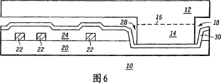
Partial sectional view among Fig. 6 has been represented a kind of alternate embodiment of the present invention, and in this embodiment, a kind of semi-conducting material is optionally shifted, is bonded on the dielectric layer, and this dielectric layer is along the channel layout on Semiconductor substrate;
Partial sectional view among Fig. 7 has been represented a kind of alternate embodiment of the present invention, and in this embodiment, a kind of semi-conducting material is optionally shifted, is bonded on the dielectric layer, and this dielectric layer is formed on one and has been shaped on the Semiconductor substrate of depression; And
Fig. 8 has represented the semiconductor device that another execution mode is made according to the present invention to the partial sectional view among Figure 11, in semiconductor device, carrying out the location of bonding with second half conductor layer, semiconductor is admitted on the substrate and has been set up a prosthesis structure (dummy feature).
Describe clearly in order to simplify to describe and make, accompanying drawing has been represented the general type of structure of the present invention, simultaneously, causes unnecessary interference for fear of the understanding of the present invention, has omitted the description of well-known characteristic and technology and goes through.In addition, the element in the accompanying drawing there is no need proportionally to draw.By way of example, some size of component has been exaggerated with respect to other element among the figure, helps the understanding to embodiment of the present invention.In addition, identical reference numbers components identical in the different accompanying drawings.
In addition, if necessary, used words such as " first, second " in specification and claims, these words are used to distinguish similar elements, but are not to be in order to describe order or chronological order.It is also understood that: under suitable environment, the use of these words is interchangeable, thereby the embodiment of the present invention described in the literary composition for example can be carried out according to being different from the literary composition order represented or that describe order.
In addition, if necessary, used word in specification and claims in order to be described such as " forward and backward, top, bottom, upper and lower " etc., but these words and infinite be immutable relative position relation.Be understood that under suitable environment, the use of these words is interchangeable, thereby the embodiment of the present invention described in the literary composition for example can be carried out according to being different from the literary composition orientation represented or orientation described.
Embodiment
Generally speaking, the present invention both had been directed to and has been bonded to on-plane surface and admits the problem of substrate, also only be directed to problem in the selected position formation bonding zone of admitting substrate.In one embodiment, a donor substrate is made into to comprise a jut (hereinafter being referred to as donor mesa), admits on the substrate so that have only this jut to be transferred to.Thereby, admit substrate to lack flatness of overall importance and can't the para-linkage process cause adverse effect.In addition, by corresponding depression being set admitting on the substrate, can make the final structure behind the bonding have higher flatness.In another embodiment, admit substrate to be provided with a prosthesis structure, it can be raised effectively and admit the zone of wanting second half conductor material of bonding on the substrate.By making all the other structures of admitting the zone of wanting second half conductor material of bonding on the substrate to be higher than to admit on the substrate or contour with all the other structures at least, can guarantee at the enough strong bonding action of this zone acquisition.
Fig. 1 has represented manufacture process according to an embodiment of the present invention, that form semiconductor device 10 to Fig. 4 with the form of part sectioned view.In Fig. 1, provide a donor substrate 12.The matrix of donor substrate 12 preferably is made up of semiconductor single crystal material, and these materials for example are silicon, germanium, GaAs, indium phosphide etc.In the application scenario of the present invention described in a preferred implementation and the whole application, donor substrate all is made up of germanium.As can be seen from Figure 1, donor substrate 12 has an injection region 14, and this injection region for example is by forming in the surface that hydrogen ion is injected into donor substrate 12.The purpose that forms injection region 14 is in order to form a transfer layer, and this skim donor substrate can be transferred on another substrate.Also can select for use other method to form transfer layer.For example, can on the surface of donor substrate, make a lattice layer with strain, can on this strain lattice layer, produce a transfer layer.
The degree of depth or the thickness of injection region 14 can be chosen as the expection thickness that equals to be transferred to the semi-conducting material on the admittance substrate.The injection energy is chosen to be and makes the drop shadow spread or the peak concentration (shown in the dotted line 15 of Fig. 1) that inject element equal the required degree of depth.Usually, this depth bounds to 0.1 μ m between the 2 μ m, implantation dosage is 1 * 10
16To 1 * 10
17Between atom/cubic centimetre.In a preferred embodiment, the material that is transferred is used as photoelectricity testing part, in the case, preferably protium is injected in the germanium wafer, and injecting the degree of depth is that 1 μ m is to 2 μ m.
(no matter being by injecting or other technology formation) carries out composition to donor substrate 12, so that transfer layer only appears at selected zone after forming transfer layer.As shown in Figure 1, this work is finished like this: form an etching mask 16 by deposit and composition one photoresist layer, it is protecting the transfer layer that is positioned at selection area.Then, as shown in Figure 2, as etching mask donor substrate is carried out etching and formed a donor mesa 18 with etching mask 16.Preferably, donor substrate 12 is etched to the injection region 14 that (does not promptly comprise) and all is removed except that donor mesa 18, thereby has only the material in the donor mesa 18 can be transferred to from donor substrate 12 on the admittance substrate.Zone except that donor mesa is called as the matrix part of substrate.Conventional chemical etchant and technology can be used to carry out this etching processing, and concrete chemical agent and technology depend on the certain material on the donor substrate 12.In a preferred embodiment, donor substrate 12 comprises the germanium after hydrogen ion injects, and a kind of etching agent that is suitable for forming donor mesa 18 is chloride or fluorine plasma chemical etching agent.As alternative, can adopt such as containing hydrogen peroxide (H
2O
2) the wet etch chemistries of the aqueous solution etc. form donor mesa 18.Although only expressed a donor mesa 18 in the drawings, this area engineering staff can recognize and can form arbitrary number such table top.
In an alternate embodiment, substrate carry out is injected or other processing, with before forming transfer layer, can carry out composition to donor substrate 12, so that form one or more donor mesa.In this alternate embodiment, hydrionic injection occurs in after table top forms, and the height of table top and injection situation be adjusted to the material that only allows in the mesa region and can be transferred to and admit on the substrate, can more clearly understand these contents from introduction hereinafter.
After the donor substrate 12 after forming or composition is provided in addition, the donor substrate behind the composition is bonded to admits on the substrate 20 as shown in Figure 3.Preferably, admit the matrix of substrate to be made up of semiconductor single crystal material, these materials for example are silicon, germanium, GaAs, indium phosphide etc.In a preferred implementation, admit substrate 20 to constitute by silicon.Admit substrate 20 can comprise active or/or passive device, these devices or in the substrate-based block of material or on matrix.For understanding the present invention, the concrete condition of these devices is unimportant.Therefore, selected several representative elements have only been expressed in the drawings.By way of example, as shown in Figure 3, admit substrate 20 to comprise a plurality of conductive members 22, these conductive members have first a stacked dielectric layer 24.According to the practice form of routine, conductive member can be made by polysilicon or metal.Equally, can utilize technique known to make dielectric layer 24, in a preferred embodiment, dielectric layer comprises silicon dioxide (SiO
2) material.
From Fig. 3 as seen, like that, admitting the surface of substrate 20 is on-plane surface in the so susceptible condition.Therefore, be used in the prior art can there be aforesaid problem in the technology that second half conductive substrate is bonded on it.According to the present invention, just can overcome these problems by the alms giver's Semiconductor substrate behind the composition being bonded to admit on the substrate.More specifically, donor substrate 12 is by so positioned with respect to admitting substrate 20: make donor mesa 18 be about on the substrate 20 admit the part that is transferred layer to align with admitting.As shown in the figure, donor mesa is arranged into and can not covers any active circuit of admitting on the substrate 20, and still, this is not to be the requirement condition of all application scenarios of the present invention.
After donor mesa 18 is aimed at fully, admit substrate 20 and donor substrate 12 to be bonded to together at the contact area place, contact area wherein that is to say donor mesa and the contacted zone of upper surface of admitting substrate 20.Can utilize known wafer bonding techniques to realize bonding, form the sufficiently high engagement keys of intensity but will adopt a Pressure/Temperature to handle usually.The material that exists in donor substrate 20 or the admittance substrate 12 may limit and adopt how high bonding temperature and processing subsequently.In addition, the present invention does not make restriction to specific bonding techniques.
Should be noted that:, be not such situation usually although the left side of donor substrate 20 seems not to be supported on the device 10 in Fig. 3.Preferably, donor substrate 12 and admittance substrate 20 are the form of wafer, all have a plurality of positions that are provided with device on each wafer.Therefore, donor substrate 12 probably is subjected to admitting the support of at least one adjacent device position on the substrate, even may be subjected to the support of position on the device 10 elsewhere.If underbraced then is provided with some table tops in addition other support structure effect is provided.
In case donor substrate 12 is just carried out a separating step or transfer step after being bonded to and admitting on the substrate 20.In this step, as shown in Figure 4, the matrix of donor substrate 12 partly is removed.In other words, removing the injection region 14 that is bonded to the donor mesa 18 on the admittance substrate 12, remaining donor substrate 12 all is removed.The result has just formed a transfer layer 26.Can utilize technique known that the remainder of transfer layer and donor substrate 12 is separated.By way of example, can adopt the hot working technology, in this technology, form bubble hydrogen at the peak concentration place (15 expressions of figure with dashed lines) that hydrogen injects.Bubble have a separation that is beneficial to transfer layer this position in donor mesa 18.As alternative, can adopt mechanical means to impel the separation at same area place in the donor mesa, for example can adopt methods such as ultrasonic vibration, fluid injection to carry out cracking.
After the transfer layer 26 and the remainder of donor substrate 12 are separated, can on transfer layer 26, form device, and make line for it.In a preferred embodiment,, and between the two, form non-doped region, just can utilize transfer layer 26 to form a photodetector by the conductive finger of transplanting N type and P type.And then the formation line, so that conductive finger and the circuit in admitting substrate 20 couple together.
The present invention with reference to the described execution mode of Fig. 1-4 in, donor mesa 18 is bonded on the dielectric layer 24 of admitting substrate 20, and not for admitting donor mesa to make any specific contained structure.In an alternate embodiment, be that cavity is held in donor mesa formation one to admitting substrate 20 to carry out processing, thereby the structure that causes finally making have higher flatness.In some applications, the expection thickness of transfer layer 26 is very big, to such an extent as to make the flatness of the structure after final bonding/transfer be not enough to carry out subsequently processing.In order to tackle so thick transfer layer, admit the depression in the substrate can be made with the suitable degree of depth, to reach sufficiently high final flatness.For example, in Fig. 5, dielectric layer 24 is carried out composition and forms an opening 27, it exposes the surface of the matrix semi-conducting material of admitting substrate 20.As alternative, as shown in Figure 6, can in the bulk material of admitting substrate 20, form a cavity or groove 28.Perhaps can carry out etching and form a depression 32 dielectric layer 24 as shown in Figure 7, this depression can't expose the understructure of admitting substrate 20.In arbitrary execution mode of Fig. 5-7, can make according to known lithographic technique and admit cavity (no matter be opening 27, groove 28 or cave in 32), concrete lithographic technique will depend on the removed material of needs.
Shown in execution mode among Fig. 5, donor mesa 18 is bonded on the matrix of admitting substrate 20 (being that this is that a semiconductor is to semi-conductive engagement keys), rather than is bonded on the dielectric material.Obtain in hope in the occasion of heterostructure device (for example germanium the structure on the silicon, the InGaAsP structure on GaAs etc.), such design is favourable.Avoid or reduce forming bulk oxidation thing layer on exposed semiconductor surface in order to realize semiconductor to semi-conductive bonding, to should be noted that, this oxide skin(coating) can reduce bond strength or influence the work of heterojunction device.
Above-mentioned various alternative in any, donor mesa is bonded to admit on the substrate 20 before, dielectric layers 30 of the one optional character of deposit thereon all.Dielectric layer 30 can be used to form electric insulation between two backing materials (as shown in Figure 6) or strengthen bonding action between two substrates.Be suitable for comprising SiO as the material of dielectric layer 30
2, the SiO that fluoridizes
2, benzocyclobutene (BCB), MSSQ (methysilsequioxane) and other be used for the material of bonding " bonding layer ".If adopt dielectric layer 30, the technology of available routine comes it is carried out deposit.
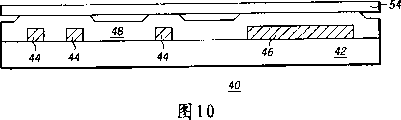
Be introduced with reference to Fig. 8-11 pair of a kind of alternative methods below, this method is used to solve and admits the relevant problem of execution bonding on the substrate at on-plane surface, and these accompanying drawings have also been represented a kind of according to processing method of the present invention, that be used to form semiconductor device 40.As shown in Figure 8, admit substrate 42 to comprise conductive member 44 and one first dielectric layer 48.These elements are similar to admittance substrate 20, conductive member 22 and first dielectric layer 24 in the last execution mode respectively.In addition, admit substrate 42 to comprise a prosthesis structure 46, it is formed in will be from the position that donor substrate 50 shifts a layer body.Expressed donor substrate 50 among Fig. 9, it is the same with aforesaid donor substrate 12, single-crystal semiconductor material preferably, and comprise an injection region 52, and also having the peak concentration district of injection element (being preferably hydrogen), it is in the drawings by dotted line 53 expressions.
According to the present invention, as shown in Figure 9, the admittance substrate 42 with prosthesis structure 46 is bonded on the donor substrate 50.Can donor substrate 50 be bonded to according to above-mentioned method and admit on the substrate 42, and preferably, only produce bonding in the location (comprising the zone on the prosthesis structure 46) that two substrates are in contact with one another.
As shown in figure 10, the matrix of donor substrate 50 partly is removed, and only stays one and is covered with the transfer layer 54 of admitting substrate 42 whole surfaces.Preferably, this removal process is to adopt above with reference to a certain technology of removing in the described several technology of donor substrate 12 matrix parts to finish.As alternative, also can adopt the back-etching technology.Then, as shown in figure 11, offscreen method is carried out composition and etching processing to transfer layer 54, thereby stays the transfer layer 56 of a composition on prosthesis structure 46.Can process and form a device the transfer layer behind the composition, this device for example be the optics of photodetector etc., its with built in admitting the circuit on the substrate 42 to keep being electrically connected.
Thereby obviously: the application provides a kind of improved substrate bonding method, and this method can be applicable to on-plane surface and admits on the substrate, and in addition, it has also realized optionally bonding.The donor mesa of utilization on donor substrate optionally transferred to semi-conducting material and admitted on the substrate.Admit substrate need not have very high flatness, it can be changed to having a table top and admit depression, so that further improve the flatness of final structure behind the bonding.Aspect the thickness that is transferred layer body, manufacture method proposed by the invention has the control ability of height.In addition, the present invention especially is beneficial to dissimilar semi-conducting material will be bonded to together occasion, and reason is and can synchronously processes, rather than in turn the device of certain semi-conducting material is bonded on second half conductor material.The donor mesa semi-conducting material is transferred to the design of admitting one or more selection areas on the substrate and forming a plane after table top shifts help subsequently integrated circuit procedure of processing, follow-up step is both at some part of donor substrate, also at some part of admitting substrate.For example, can make metal layer or interlayer dielectric layer with admitting on the substrate part in the donor mesa part of entire semiconductor device.
Above effect of the present invention, other advantage and the scheme of dealing with problems are described at concrete execution mode.But, that these effects, advantage, the scheme of dealing with problems and any other factors all should not be construed as in some or all claim is necessary, required or important feature or factor, and other factors wherein can bring any effect, advantage or scheme obvious or that become obvious.In the linguistic context of this paper, word " comprises ", other modification of " comprising " or these words is used to express the open of non-exclusionism and contains, for example, the technology, method, article or the device that comprise listed element not only comprise these elements, but also may comprise the element that other is not listed, or these methods, technology, article or install intrinsic element.
In description above, invention has been described with reference to concrete execution mode.But those of ordinary skills can understand: under the prerequisite departing from the scope of the invention not, can make the change and the modification of various ways, wherein, scope of the present invention is limited by the accompanying Claim book.By way of example, those of ordinary skill can be recognized and one or several aspect in described arbitrary execution mode can be combined (for example donor mesa can be used in combination with prosthesis structure) with another execution mode.In addition, those skilled in the art will recognize that: donor substrate with the acceptor wafer bonding before, can be shaped on therein device or the part device.In addition, before donor substrate being bonded on the admittance substrate, can in admitting substrate, be shaped on the device of device or part.In addition, donor substrate is bonded to admit on the substrate after, can carry out the manufacturing that each step well known in the art is finished integrated circuit.Therefore, the description of this paper and accompanying drawing only are counted as exemplary, but not determinate, and the present invention cover all remodeling forms.
Claims (3)
1. the bonding method of a substrate comprises:
In donor substrate, inject a kind of element and form the injection region;
Donor substrate is carried out composition and formed matrix part and donor mesa, and wherein, donor mesa comprises at least a portion of described injection region;
The admittance cavity that utilizes donor mesa and admit substrate to comprise arrives donor substrate with the admittance substrate bonding; And
Remove the matrix part of donor substrate, but stay the transfer layer of donor substrate, it is bonded in admitting cavity admits on the substrate,
Wherein said transfer layer comprises described donor mesa.
2. method that forms semiconductor device comprises:
First Semiconductor substrate is bonded on second Semiconductor substrate, and wherein, second Semiconductor substrate comprises:
The first area;
Second area; And
Be formed in the prosthesis structure in the first area, this prosthesis structure make the first area end face at least with the end face of second area on the highest part contour;
Get rid of the part of first Semiconductor substrate, thereby form the transfer layer on the first area that is bonded to second Semiconductor substrate; And
Transfer layer is carried out composition, so that on prosthesis structure, form the transfer layer part that is furnished with pattern, and get rid of a part of described transfer layer from the second area of second Semiconductor substrate.
3. the bonding method of a substrate comprises:
First Semiconductor substrate is set, wherein, first Semiconductor substrate is carried out composition and formed table top and matrix part;
Second Semiconductor substrate is set, and wherein, the pattern of second Semiconductor substrate is an on-plane surface, and second Semiconductor substrate comprises the admittance cavity;
First Semiconductor substrate and the second Semiconductor substrate bonding are got up, and wherein, described bonding also comprises table top is bonded to the operation of admitting in the cavity; And
Get rid of the matrix part of first Semiconductor substrate, stay a part of table top that is bonded on first Semiconductor substrate at least simultaneously, wherein said at least a portion table top is a transfer layer.
Applications Claiming Priority (2)
| Application Number | Priority Date | Filing Date | Title |
|---|---|---|---|
| US10/022,711 US6616854B2 (en) | 2001-12-17 | 2001-12-17 | Method of bonding and transferring a material to form a semiconductor device |
| US10/022,711 | 2001-12-17 |
Publications (2)
| Publication Number | Publication Date |
|---|---|
| CN1615543A CN1615543A (en) | 2005-05-11 |
| CN1324674C true CN1324674C (en) | 2007-07-04 |
Family
ID=21811041
Family Applications (1)
| Application Number | Title | Priority Date | Filing Date |
|---|---|---|---|
| CNB028272463A Expired - Fee Related CN1324674C (en) | 2001-12-17 | 2002-12-05 | Method for bonding and transferring a material to form a semiconductor device |
Country Status (8)
| Country | Link |
|---|---|
| US (1) | US6616854B2 (en) |
| EP (1) | EP1500132A2 (en) |
| JP (1) | JP4554930B2 (en) |
| KR (1) | KR20040079916A (en) |
| CN (1) | CN1324674C (en) |
| AU (1) | AU2002353020A1 (en) |
| TW (1) | TWI255525B (en) |
| WO (1) | WO2003052817A2 (en) |
Families Citing this family (16)
| Publication number | Priority date | Publication date | Assignee | Title |
|---|---|---|---|---|
| US7078320B2 (en) * | 2004-08-10 | 2006-07-18 | International Business Machines Corporation | Partial wafer bonding and dicing |
| US7288458B2 (en) * | 2005-12-14 | 2007-10-30 | Freescale Semiconductor, Inc. | SOI active layer with different surface orientation |
| KR100755368B1 (en) | 2006-01-10 | 2007-09-04 | 삼성전자주식회사 | Methods of manufacturing a semiconductor device having a three dimesional structure and semiconductor devices fabricated thereby |
| US7682930B2 (en) * | 2006-06-09 | 2010-03-23 | Aptina Imaging Corporation | Method of forming elevated photosensor and resulting structure |
| US7432174B1 (en) * | 2007-03-30 | 2008-10-07 | Advanced Micro Devices, Inc. | Methods for fabricating semiconductor substrates with silicon regions having differential crystallographic orientations |
| EP1993126B1 (en) * | 2007-05-18 | 2011-09-21 | Semiconductor Energy Laboratory Co., Ltd. | Manufacturing methods of semiconductor substrate |
| US8201325B2 (en) | 2007-11-22 | 2012-06-19 | International Business Machines Corporation | Method for producing an integrated device |
| US7842583B2 (en) * | 2007-12-27 | 2010-11-30 | Semiconductor Energy Laboratory Co., Ltd. | Method for manufacturing semiconductor substrate and method for manufacturing semiconductor device |
| US7927975B2 (en) | 2009-02-04 | 2011-04-19 | Micron Technology, Inc. | Semiconductor material manufacture |
| GB0914251D0 (en) * | 2009-08-14 | 2009-09-30 | Nat Univ Ireland Cork | A hybrid substrate |
| CN102822970B (en) * | 2010-03-31 | 2015-06-17 | Soitec公司 | Bonded semiconductor structures and method of forming same |
| FR2965974B1 (en) * | 2010-10-12 | 2013-11-29 | Soitec Silicon On Insulator | PROCESS FOR MOLECULAR BONDING OF SILICON AND GLASS SUBSTRATES |
| US8778737B2 (en) | 2011-10-31 | 2014-07-15 | International Business Machines Corporation | Flattened substrate surface for substrate bonding |
| US9190379B2 (en) | 2012-09-27 | 2015-11-17 | Apple Inc. | Perimeter trench sensor array package |
| US9209142B1 (en) * | 2014-09-05 | 2015-12-08 | Skorpios Technologies, Inc. | Semiconductor bonding with compliant resin and utilizing hydrogen implantation for transfer-wafer removal |
| WO2017052646A1 (en) * | 2015-09-25 | 2017-03-30 | Intel Corporation | Island transfer for optical, piezo and rf applications |
Citations (3)
| Publication number | Priority date | Publication date | Assignee | Title |
|---|---|---|---|---|
| US6093623A (en) * | 1998-08-04 | 2000-07-25 | Micron Technology, Inc. | Methods for making silicon-on-insulator structures |
| CN1272684A (en) * | 1999-02-02 | 2000-11-08 | 佳能株式会社 | Substrate and its manufacturing method |
| US6191007B1 (en) * | 1997-04-28 | 2001-02-20 | Denso Corporation | Method for manufacturing a semiconductor substrate |
Family Cites Families (11)
| Publication number | Priority date | Publication date | Assignee | Title |
|---|---|---|---|---|
| US4966646A (en) | 1986-09-24 | 1990-10-30 | Board Of Trustees Of Leland Stanford University | Method of making an integrated, microminiature electric-to-fluidic valve |
| US5389569A (en) * | 1992-03-03 | 1995-02-14 | Motorola, Inc. | Vertical and lateral isolation for a semiconductor device |
| JP3114570B2 (en) * | 1995-05-26 | 2000-12-04 | オムロン株式会社 | Capacitive pressure sensor |
| JPH09127352A (en) * | 1995-10-30 | 1997-05-16 | Hitachi Ltd | Semiconductor device and its production |
| JP3257624B2 (en) * | 1996-11-15 | 2002-02-18 | キヤノン株式会社 | Semiconductor member manufacturing method |
| JPH1140823A (en) * | 1997-05-22 | 1999-02-12 | Fujitsu Ltd | Photodetector module |
| JPH1145862A (en) * | 1997-07-24 | 1999-02-16 | Denso Corp | Manufacture of semiconductor substrate |
| US6271101B1 (en) * | 1998-07-29 | 2001-08-07 | Semiconductor Energy Laboratory Co., Ltd. | Process for production of SOI substrate and process for production of semiconductor device |
| JP2001007362A (en) * | 1999-06-17 | 2001-01-12 | Canon Inc | Semiconductor substrate and manufacture of solar cell |
| JP2001102523A (en) * | 1999-09-28 | 2001-04-13 | Sony Corp | Thin-film device and manufacturing method therefor |
| US6400009B1 (en) * | 1999-10-15 | 2002-06-04 | Lucent Technologies Inc. | Hermatic firewall for MEMS packaging in flip-chip bonded geometry |
-
2001
- 2001-12-17 US US10/022,711 patent/US6616854B2/en not_active Expired - Fee Related
-
2002
- 2002-12-05 KR KR10-2004-7010056A patent/KR20040079916A/en not_active Application Discontinuation
- 2002-12-05 WO PCT/US2002/038564 patent/WO2003052817A2/en active Application Filing
- 2002-12-05 EP EP02789986A patent/EP1500132A2/en not_active Withdrawn
- 2002-12-05 JP JP2003553615A patent/JP4554930B2/en not_active Expired - Fee Related
- 2002-12-05 AU AU2002353020A patent/AU2002353020A1/en not_active Abandoned
- 2002-12-05 CN CNB028272463A patent/CN1324674C/en not_active Expired - Fee Related
- 2002-12-16 TW TW091136258A patent/TWI255525B/en not_active IP Right Cessation
Patent Citations (3)
| Publication number | Priority date | Publication date | Assignee | Title |
|---|---|---|---|---|
| US6191007B1 (en) * | 1997-04-28 | 2001-02-20 | Denso Corporation | Method for manufacturing a semiconductor substrate |
| US6093623A (en) * | 1998-08-04 | 2000-07-25 | Micron Technology, Inc. | Methods for making silicon-on-insulator structures |
| CN1272684A (en) * | 1999-02-02 | 2000-11-08 | 佳能株式会社 | Substrate and its manufacturing method |
Also Published As
| Publication number | Publication date |
|---|---|
| CN1615543A (en) | 2005-05-11 |
| WO2003052817A3 (en) | 2003-08-21 |
| TWI255525B (en) | 2006-05-21 |
| AU2002353020A1 (en) | 2003-06-30 |
| TW200302548A (en) | 2003-08-01 |
| WO2003052817A2 (en) | 2003-06-26 |
| EP1500132A2 (en) | 2005-01-26 |
| WO2003052817B1 (en) | 2003-09-25 |
| JP2005513781A (en) | 2005-05-12 |
| JP4554930B2 (en) | 2010-09-29 |
| US20030114001A1 (en) | 2003-06-19 |
| AU2002353020A8 (en) | 2003-06-30 |
| KR20040079916A (en) | 2004-09-16 |
| US6616854B2 (en) | 2003-09-09 |
Similar Documents
| Publication | Publication Date | Title |
|---|---|---|
| CN1324674C (en) | Method for bonding and transferring a material to form a semiconductor device | |
| CN1155073C (en) | Insulator base silicon structure of plane dense picture composition and manufacture technology thereof | |
| CN1836323A (en) | High-performance CMOS SOI device on hybrid crystal-oriented substrates | |
| CN1838417A (en) | Semiconductor structure and its forming method | |
| KR970030640A (en) | Method of forming device isolation film in semiconductor device | |
| CN1280913C (en) | Semiconductor chip on insulator and its manufacture | |
| KR100366748B1 (en) | Stencil mask and method of forming the same | |
| KR100511900B1 (en) | Method of manufacturing SOI substrate | |
| KR20010060988A (en) | Manufacturing method for isolation in semiconductor device | |
| JP3216488B2 (en) | Method for manufacturing semiconductor device | |
| KR20210056831A (en) | Producing method of silicon on insulator substrate | |
| KR0179022B1 (en) | Method for isolating semiconductor device | |
| KR950009922A (en) | Contact structure of semiconductor device and manufacturing method thereof | |
| KR100318262B1 (en) | Method for forming alignment key of semiconductor device | |
| KR20020002640A (en) | A method for a field oxide of semiconductor device | |
| KR20210111488A (en) | Producing method of multi silicon on insulator substrate and multi silicon on insulator substrate | |
| KR19990032753A (en) | Semiconductor Device Separation Method | |
| US20030022458A1 (en) | Method for forming a shallow trench isolation in a semiconductor structure | |
| KR950029849A (en) | Device Separator Formation Method | |
| KR950012680A (en) | Device Separation Method of Semiconductor Device | |
| KR20070090089A (en) | Semiconductor device and manufacturing method thereof | |
| KR950021349A (en) | Quasi-magnetic alignment trench isolation method | |
| KR19980055926A (en) | Manufacturing method of semiconductor device | |
| KR20040001326A (en) | Method for forming the Isolation Layer of Semiconductor Device | |
| KR20080051684A (en) | Method of forming semiconductor devic |
Legal Events
| Date | Code | Title | Description |
|---|---|---|---|
| C06 | Publication | ||
| PB01 | Publication | ||
| C10 | Entry into substantive examination | ||
| SE01 | Entry into force of request for substantive examination | ||
| C14 | Grant of patent or utility model | ||
| GR01 | Patent grant | ||
| C56 | Change in the name or address of the patentee |
Owner name: FISICAL SEMICONDUCTOR INC. Free format text: FORMER NAME: FREEDOM SEMICONDUCTOR CORP. |
|
| CP01 | Change in the name or title of a patent holder |
Address after: Texas in the United States Patentee after: FREESCALE SEMICONDUCTOR, Inc. Address before: Texas in the United States Patentee before: FreeScale Semiconductor |
|
| CF01 | Termination of patent right due to non-payment of annual fee |
Granted publication date: 20070704 Termination date: 20141205 |
|
| EXPY | Termination of patent right or utility model |