CN1296755C - Electro-optical device in installing shell and projecting displaying device - Google Patents
Electro-optical device in installing shell and projecting displaying device Download PDFInfo
- Publication number
- CN1296755C CN1296755C CNB2003101218208A CN200310121820A CN1296755C CN 1296755 C CN1296755 C CN 1296755C CN B2003101218208 A CNB2003101218208 A CN B2003101218208A CN 200310121820 A CN200310121820 A CN 200310121820A CN 1296755 C CN1296755 C CN 1296755C
- Authority
- CN
- China
- Prior art keywords
- electro
- optical device
- mentioned
- mounting shell
- double
- Prior art date
- Legal status (The legal status is an assumption and is not a legal conclusion. Google has not performed a legal analysis and makes no representation as to the accuracy of the status listed.)
- Expired - Fee Related
Links
Images


Classifications
-
- G—PHYSICS
- G03—PHOTOGRAPHY; CINEMATOGRAPHY; ANALOGOUS TECHNIQUES USING WAVES OTHER THAN OPTICAL WAVES; ELECTROGRAPHY; HOLOGRAPHY
- G03B—APPARATUS OR ARRANGEMENTS FOR TAKING PHOTOGRAPHS OR FOR PROJECTING OR VIEWING THEM; APPARATUS OR ARRANGEMENTS EMPLOYING ANALOGOUS TECHNIQUES USING WAVES OTHER THAN OPTICAL WAVES; ACCESSORIES THEREFOR
- G03B21/00—Projectors or projection-type viewers; Accessories therefor
- G03B21/14—Details
- G03B21/20—Lamp housings
-
- H—ELECTRICITY
- H04—ELECTRIC COMMUNICATION TECHNIQUE
- H04N—PICTORIAL COMMUNICATION, e.g. TELEVISION
- H04N9/00—Details of colour television systems
- H04N9/12—Picture reproducers
- H04N9/31—Projection devices for colour picture display, e.g. using electronic spatial light modulators [ESLM]
- H04N9/3141—Constructional details thereof
- H04N9/3144—Cooling systems
Abstract
The invention relates to an optoelectronic device accommodated in installing enclosure, which comprises the optoelectronic device that projects light from the light source at image display area, a panel installed oppositely to one side of the optoelectronic device and the cover covering the said optoelectronic device and connected with the said panel. At least one part of the peripheral area of the said image display area located at the said optoelectronic device that is kept in one of the said panel and the said cover accommodates the installing enclosure of the optoelectronic device. At least one of the said panel and the said cover is bonded with the said optoelectronic device with bonding method.
Description
Technical field
The present invention relates in the mounting shell that is used for installing the electro-optical devices such as liquid crystal panel that are used in projection type image display apparatus such as liquid crystal projector as light valve, install or contain this electro-optical device forms place the electro-optical device in the mounting shell and possess such projection type image display apparatus that places the electro-optical device in the mounting shell.
Background technology
Usually, under using the situation of liquid crystal panel as the light valve in the liquid crystal projector, this liquid crystal panel can not be set at for example exposed state in the housing that constitutes liquid crystal projector etc., but after this liquid crystal panel being installed or be housed in the suitable mounting shell, place the liquid crystal panel in the mounting shell to be arranged on above-mentioned housing etc. this.
This is because by suitable screw hole etc. is set on this mounting shell in advance, can implement easily liquid crystal panel to above-mentioned housing etc. fixing, install.
In this liquid crystal projector, the light source light of sending from light source places liquid crystal panel in the mounting shell to be throwed by the state behind the optically focused to this.And the light that sees through liquid crystal panel is exaggerated and is incident upon on the screen to carry out the demonstration of image.Like this,, generally be redefined for and amplify projection, so for example just need to use stronger light from light emitted such as metal halid lamps as above-mentioned light source light because in liquid crystal projector.
So, the problem that has at first occurred placing liquid crystal panel, especially liquid crystal panel temperature in the mounting shell to rise.That is, rise if produce this temperature, the temperature that then is clamped in the liquid crystal between a pair of transparency carrier in liquid crystal panel also rises, and will cause the deterioration of this liquid crystal characteristic.In addition, particularly occur under the uneven situation in light source light, liquid crystal panel is partly heated and is produced so-called heat spot, causes the inequality of the transmissivity of liquid crystal, thereby makes the quality deterioration of projects images.
Technology as the intensification that prevents this liquid crystal panel, have a kind of by liquid crystal panel and accommodate and support this liquid crystal panel and possess simultaneously in the LCD MODULE that housing that heat sink is arranged constitutes, by between above-mentioned liquid crystal panel and above-mentioned heat sink, heat radiator being set, with the technology of the intensification that prevents liquid crystal panel.
In addition, in order to address this is that, in addition also known having is provided with photomask, is made of the technology such as mounting shell of installing or taking in liquid crystal panel light reflective material on the substrate of the light incident side that is positioned at liquid crystal panel.
But, have following problem in the countermeasure that liquid crystal panel heats up existing preventing.Promptly, as long as the high light projection from light source light is arranged, the problem that the temperature of liquid crystal panel rises just might often display, therefore in order to seek further high image qualityization etc., require to replace above-mentioned various countermeasures or on this, propose the countermeasure that prevents that more effectively temperature from rising.
In addition, for above-mentioned each prevent that from all there is following difficult point in the countermeasure that heats up.That is, in utilizing the countermeasure of above-mentioned heat radiator, though can think really and can be effectively to be accumulated in heat in the liquid crystal panel to the outside radiation, for the location of the liquid crystal panel in the housing but without any effective function.That is, if utilize heat radiator, then the intensification of liquid crystal panel will inevitably cause the intensification of housing, if but like this, because linear expansion coefficient not equal of the two, can notify the offset of the liquid crystal panel that causes this enclosure interior.
And then, if heat sink or heat radiator are set to prerequisite in the mode that covers whole base plate, though then also can utilize in reflexive liquid crystal panel, powerless for the liquid crystal panel of transmission-type.
In addition, in utilizing the light reflection countermeasure of photomask and mounting shell, though can think if make they the area increase reflection light quantity will increase, therefore that can realize correspondingly really that the temperature of liquid crystal panel rises prevents, if but exceedingly increase reflection light quantity, the parasitic light of taking in this housing that places the liquid crystal panel in the mounting shell is increased, the quality of image is brought ill effect.In addition, for photomask, its area is big more, and the amount that should incident sees through the light source light of liquid crystal panel will reduce, and well imagines to cause the image deepening.This just shows bright more image and uses the purport of stronger light source light to disagree with hope.Like this, above-mentioned countermeasure has and can't say and fundamentally solved the such problem of problem.
Summary of the invention
The present invention proposes in view of the above problems, its purpose is to provide a kind of electro-optical device in the mounting shell of placing of the offset of avoiding the electro-optical device in the mounting shell as much as possible, in addition, also provide that a kind of temperature that can effectively suppress incident and have the electro-optical device of stronger projection light rises, place the electro-optical device in the mounting shell and possess its projection type image display apparatus.
The interior electro-optical device of mounting shell that places of the present invention has in order to solve above-mentioned problem, to possess: the electro-optical device that projection light is arranged from light source incident on image display area; And be made up of with the lid that covers above-mentioned electro-optical device and have a position that contacts with above-mentioned plate the plate that relatively disposes with the one side of this electro-optical device, and at least a portion of neighboring area that keeps the periphery that is arranged in above-mentioned image display area in the above-mentioned electro-optical device with at least one side in above-mentioned plate and the above-mentioned lid is to take in the mounting shell of this electro-optical device.And at least one side and above-mentioned electro-optical device in above-mentioned plate and the above-mentioned lid carry out bonding via adhering device.
If adopt the electro-optical device that places in the mounting shell of the present invention, then on image display area, be installed in the mounting shell of forming by lid and plate from the electro-optical device of light source incident by projection light.Can list liquid-crystal apparatus or the liquid crystal panel that for example is mounted as this electro-optical device as the light valve in the projection type image display apparatus.Have again, in this mounting shell,, it is had prevent the exposure in this neighboring area or prevent the shade function that parasitic light enters from the neighboring area in the image display area etc. by covering the neighboring area of electro-optical device at least in part.
And, in the present invention, especially, at least one side in above-mentioned plate and the above-mentioned lid (below, in explanation) and above-mentioned electro-optical device for easy and use " plate " side representative about the present invention and various forms thereof via adhering device by bonding.Thus, at first because can form between the two fixing (bonding) more reliably, so can prevent from mounting shell, to cause the situation of the offset of electro-optical device effectively by cementability that adhering device had.Especially, when this being placed electro-optical device in the mounting shell be assembled in the projection type image display apparatus such as liquid crystal projector etc., can think is having bigger pulling force from the extended flexible connector effect of electro-optical device, but in the present invention, owing to have above-mentioned adhering device, even can obtain the such advantage of offset that above-mentioned bigger pulling force can not cause the electro-optical device in the mounting shell easily yet.
In addition, if this adhering device has suitable heat conductivity, then can realize from the heat conduction of electro-optical device to plate fluently.Therefore, be subjected under the situation that temperature rises, can this heat being escaped on the plate effectively at this electro-optical device by adhering device from the light incident of light source light.
Like this, adopt the present invention can obtain the such both sides' of the effective cooling of fixing (bonding) of the electro-optical device in the mounting shell and this electro-optical device action effect simultaneously.
In a form that places the electro-optical device in the mounting shell of the present invention, above-mentioned adhering device comprises at least one side in double-sided belt and the moulding material.
According to this form, above-mentioned adhering device comprises at least one side in double-sided belt and the moulding material.Here, so-called double-sided belt is meant that tow sides have the belt of viscosity respectively, and so-called moulding material is meant the bonding agent that is for example formed by silicone resin.Thus, can form fixing (bonding) between plate and the electro-optical device more easily.
Have again, the shape in zone of the concrete shape of said in this form " double-sided belt " or coating moulding material, promptly effect has the shape in the zone of bonding force between plate and electro-optical device, can do various settings.For example, as described later, double-sided belt or moulding material are set accordingly, can in this whole zone, realize bonding between electro-optical device and the plate by whole zone with above-mentioned neighboring area.
In addition, while by respectively along reaching of the substrate that constitutes electro-optical device relative with it double-sided belt or moulding material be set with like that for example being strip, can realize bonding between electro-optical device and the plate.In addition, here so-called " constituting the substrate of electro-optical device ", be under the situation of liquid crystal indicator for example at this electro-optical device, the a pair of substrate that is equivalent to the clamping liquid crystal layer and disposes relatively, more particularly, be equivalent to be possess has as the tft array substrate of the thin film transistor (TFT) of on-off element etc. and relative substrate etc. rectangularly, or be equivalent to be provided with on any one party in described a pair of substrate or the not relative side among the both sides with above-mentioned liquid crystal layer dustproof with substrate etc.Have again, directly bonding with double-sided belt or moulding material, what can typically be susceptible to is with respect to described a pair of substrate or dustproofly carries out with substrate etc.That is, " between electro-optical device and plate bonding " is typically consistent with " constitute between the substrate of electro-optical device and the plate bonding ".
As mentioned above, if adopt the form that double-sided belt only is set in the neighboring area,, also can realize bonding between this electro-optical device and plate preferably even the electro-optical device among the present invention is so-called " transmission-type ".
But the present invention has got rid of the concrete shape of double-sided belt and the roughly the same situation of aforesaid substrate area on one's own initiative.Even in this case, " electro-optical device " that needs only among the present invention is that reflection-type is then effectively same.
In a kind of form that places the electro-optical device in the mounting shell of the present invention, at least one side in above-mentioned double-sided belt and the moulding material is made of the material with 0.6 (W/mK) or its above heat-conduction coefficient.
According to this form, because at least one side in double-sided belt and the moulding material is made of the material with the above heat-conduction coefficient of 0.6 (W/mK) or its, so the heat that is transmitted to double-sided belt or moulding material from electro-optical device can be transmitted on the plate apace again.Therefore, adopt this form can carry out the cooling of electro-optical device more effectively.
Have again, as " double-sided belt " that satisfy this condition, the band that comprises the heat conductivity silicone rubber for example arranged, adopt and comprise this heat conductivity silicone rubber and at adhesive linkage with changed the band etc. of the sandwich construction of its material on by adhesive linkage.In addition, as " moulding material " silicone RTV rubber etc. is arranged.
In other forms that place the electro-optical device in the mounting shell of the present invention, above-mentioned double-sided belt comprises ACM.
According to this form, the double-sided belt among the present invention is not above-mentioned silicone rubber, comprises ACM, can comprise the structure of metal oxide or metal nitride etc. etc. simultaneously and can adopt as main body.Such double-sided belt is also referred to as so-called acrylic acid series heat conductivity double-sided belt, and it has very excellent heat-conductive characteristic.Specifically, can obtain 1.0 (W/mK) or its above heat-conduction coefficient.
Therefore, can cool off electro-optical device more effectively according to this form.
In other forms that place the electro-optical device in the mounting shell of the present invention, at least one side of above-mentioned double-sided belt and moulding material is provided with in the corresponding mode in whole zone with above-mentioned neighboring area, and at least one side of above-mentioned plate and above-mentioned lid and above-mentioned electro-optical device are bonded together in above-mentioned whole neighboring area.
Can realize the bonding of plate and electro-optical device more reliable and more securely according to this form.In addition, because utilize the increase of the bond area of double-sided belt or moulding material, just mean and to realize more effectively, so can carry out the cooling of this electro-optical device more effectively from the conduction of electro-optical device to the heat of plate.And then, if utilize bonding electro-optical device in whole neighboring area and plate like this,, also can realize the raising of bonding force easily even then under the smaller situation of the size (can be that benchmark is considered with picture dimension (inch)) of this electro-optical device.
In other forms that place the electro-optical device in the mounting shell of the present invention, the thickness of above-mentioned double-sided belt is 50~200 (μ m).
Because adopt this form can suitably limit the thickness of above-mentioned double-sided belt, thus can guarantee the cementability of above-mentioned electro-optical device and plate more reliably, and then can carry out person's heat conduction backward effectively from the former.
Promptly, if the thickness of double-sided belt is lower than 50 (μ m), then with can because of the plate surface exist concavo-convex, promptly, constitute plate material intrinsic surfaceness " concavo-convex " that show be reason, form just like the part of above-mentioned double-sided belt is buried such state in above-mentioned concavo-convex recess, then can not make whole of this double-sided belt substrate bonding with the formation electro-optical device.In addition, its result since between aforesaid substrate and plate can with above-mentioned concavo-convex be former thereby the generation gap, so heat conduction efficiency between the two also can reduce.And in this form since the thickness of double-sided belt at 50 (μ m) or more than it, so can produce described such worry hardly.
On the other hand, if the thickness of double-sided belt surpasses 200 (μ m), though then can carry out bonding between plate and the double-sided belt respectively effectively and constitute the substrate of electro-optical device and double-sided belt between bonding, but the elasticity that may itself have because of this double-sided belt, and produce between the two relative offset.In addition, because the big more distance that then is used to conduct heat of the thickness of double-sided belt is long more, so can think that heat conduction efficiency can descend.In this form, because the thickness of double-sided belt is at 200 (μ m) or below it, so can produce described such situation hardly.
As mentioned above, because the thickness of double-sided belt in this form is restricted to 50~200 (μ m), thus can carry out bonding between plate and the electro-optical device more reliably, and, can realize the preferable heat conduction efficiency to the former from the latter.
In other forms that place the electro-optical device in the mounting shell of the present invention, at least one side in the outermost of above-mentioned plate and the outermost of above-mentioned lid is black.
According to this form, because the outermost of plate is black, so can do one's utmost to suppress this outmost light reflection.Here, comprise at the outermost that is black under the situation of face of light incident side of this plate,, do not wish the situation that takes place to the such basis of this electro-optical device incident from the light exit side of electro-optical device so can prevent light because can prevent reflection of light on this face.Thus, for example possess under a kind of situation with the substrate that can be because of so-called light leakage current make the semiconductor element that characteristic changes, can terminate in possible trouble to the light incident of this semiconductor element is anti-, and can keep its characteristic well at electro-optical device.
In addition, can avoid owing to reflected light as described above in this electro-optical device etc. again secondary reflection make this light finally sneak into situation in the image.
On the other hand, comprise at above-mentioned outermost under the situation of face of exiting side of light of this plate, can prevent the light reflection on this face, be to prevent the light of for example electro-optical device outgoing in this places mounting shell specifically, so can avoid such reflected light and sneak into situation in the image because be disposed at certain parts of its outside, for example reflection of the light that is equipped under the situation of liquid crystal projector, returns of the electro-optical device in this places mounting shell etc. because of reflection such as colour splitting prism.
According to the above,, in a word,, can go far towards to have used the demonstration of the high quality image that places the electro-optical device in the mounting shell by suppressing the light reflection on the plate if adopt this form.
Have again,, for example can be as described later the surface of this plate be imposed coating and handle, perhaps impose coating and handle for the outermost with plate is set as black.In addition, can understand from above explanation, so-called in this form " outermost " also do not mean that outmost " all " of plate.So-called should " outermost " be the term that means this plate outmost " at least a portion ".
In this form, can constitute and the surface of above-mentioned plate and at least one side in the surface of above-mentioned lid are imposed coating handle.
According to this structure, can impose plating Ni (nickel), plating Cr (chromium) or processing such as plating Zn (zinc) coating of etc.ing by surface to plate, the outermost of this plate is set as black.Like this, compare, can make the bonding force between this plate and double-sided belt stronger with handle the situation that outermost with this plate is set as black by coating.Suppose to carry out, then be easy to generate between the surface of coating and plate and peel off according to coating.Therefore, even can carry out the bonding of coating and double-sided belt securely, peel off but between coating and plate, still may produce.Yet because in this form, outermost is handled through coating and is set as black, so do not have undesirable condition as described above.
Like this, according to this form, plate and double-sided belt will be by more reliably and bonding more securely, thus, and can be more reliably and realize bonding between plate and the electro-optical device more securely.
In this structure, can further constitute after the surface of above-mentioned plate and at least one side in the surface of above-mentioned lid are imposed blasting treatment, implement above-mentioned coating again and handle.
According to this structure, can carry out above-mentioned coating and handle imposing plate surface after the blasting treatment.Here so-called blasting treatment typically refers to by the surface to a certain material and carries out particle sprayings such as iron, sand, glass, makes the processing of this surperficial state roughening.Like this, the surface that becomes coarse is called as " pears line face ".Because can form random concavo-convexly on the surface of the plate after imposing this blasting treatment usually, prevent effect so can enjoy the reflection of above-mentioned light more effectively.
Projectiveness display device of the present invention is in order to solve above-mentioned problem, possessing has: above-mentioned of the present inventionly place the electro-optical device (but, also comprising its various forms) in the mounting shell, above-mentioned light source, with the above-mentioned projection light optical system of above-mentioned electro-optical device and the projection projection optics system from the projection light of above-mentioned electro-optical device outgoing that leads.
According to this form,,, in addition, can also carry out more effectively from the heat conduction of electro-optical device to plate so can carry out fixing (bonding) between plate and electro-optical device more reliably because plate and electro-optical device be by double-sided belt or moulding material and by bonding.Therefore, the offset of the electro-optical device in the mounting shell can be prevented terminating in possible trouble, and, owing to can cool off electro-optical device effectively, so can show more high quality images.
This effect of the present invention and other benefits can be illustrated according to the example of next explanation.
Description of drawings
Fig. 1 is the planimetric map of the example of porjection type liquid-crystal apparatus of the present invention.
Fig. 2 is the planimetric map of the example of electro-optical device of the present invention.
Fig. 3 is the sectional view along the H-H ' of Fig. 2.
Fig. 4 is the three-dimensional exploded view that the mounting shell of example of the present invention and electro-optical device are together represented.
Fig. 5 is the front view that places the electro-optical device in the mounting shell of example of the present invention.
Fig. 6 is the sectional view along the X1-X1 ' of Fig. 5.
Fig. 7 is the sectional view along the Y1-Y1 ' of Fig. 5.
Fig. 8 is the rear view of observing from the Z1 direction of Fig. 5.
Fig. 9 is the front view of plate of the formation mounting shell of example of the present invention.
Figure 10 is the rear view of observing from the Z2 direction of Fig. 9.
Figure 11 is the side view of observing from the Z3 direction of Fig. 9.
Figure 12 is the stereographic map that places the electro-optical device in the mounting shell of the invention process form, and being expression places the figure of the flow direction of the wind of the electro-optical device in the mounting shell for this.
Figure 13 is the variation of representing qualitatively along with the thickness of double-sided belt, how to change from the heat conduction efficiency of electro-optical device to board or cap, in addition the curve map how to change of the position offset of this electro-optical device in mounting shell.
Figure 14 is the partial enlarged drawing of the interior part of circle of the lower left in the interior part of four circles among Fig. 7, (a) the smaller situation (being lower than the situation of 50 (μ m)) of thickness of expression double-sided belt, (b) situation that the thickness of expression double-sided belt is bigger (situation that surpasses 200 (μ m)).
Figure 15 is the figure identical with Fig. 9 purport, is the figure that represents the form different with the shape of the double-sided belt of this figure when viewed in plan, forms the situation of strip.
Figure 16 is the figure identical with Fig. 9 purport, is the figure that represents the form different with the shape of the double-sided belt of this figure when viewed in plan, is the situation that intersperses among four angles.
Label declaration
1,2 double-sided belts, 10 tft array substrates
The 20 relative substrate 400 dustproof substrates of using
50 liquid crystal layers, 500 electro-optical devices
601 boards, 615 window portions
Concavo-convex 620 caps of 610S
625 window portions, 622 cooling air introduction parts
622T tapered portion 622P wind deflector
623 lid bodies, 627 lateral fin sheet portions
Fin portion behind the 624 cooling air discharge portion 624F
100R, 100G, 100B light valve 1100 liquid crystal projectors
1102 lamp source
Embodiment
Below with reference to the accompanying drawings example of the present invention is described.
The example of porjection type liquid-crystal apparatus
At first, with reference to Fig. 1,, be that the center describes with the optical system that is assembled in its optical unit to the example of porjection type liquid-crystal apparatus of the present invention.The projection type image display apparatus of this example is constructed as the multiple-piece color projector, and this multiple-piece color projector uses the liquid crystal light valve that has three conducts to place an example of the electro-optical device in the mounting shell.
In Fig. 1, as the liquid crystal projector 1100 of an example of the multiple-piece color projector of this example, construct as the projector of preparing three liquid crystal light valves that include the electro-optical device that driving circuit has been installed on tft array substrate and its light valve 100R, 100G that uses as RGB respectively and 100B are used.
In liquid crystal projector 1100, when the lamp unit 1102 from white light sources such as metal halide lamps sends projection light, then by three catoptrons 1106 and two dichronic mirrors 1108, be divided into and the corresponding light component R of RGB three primary colors, G, B, and be directed to respectively and corresponding light valve 100R of all kinds, 100G and 100B.At this moment, the light loss of B light in order to prevent to cause because of long light path guided by the relay lens system 1121 that is made of incident lens 1122, relay lens 1123 and exit lens 1124.Then, respectively via after light valve 100R, 100G and the 100B modulation with the corresponding light component of three primary colors via colour splitting prism 1112 synthetic once more after, project on the screen 1120 as coloured image by projection lens 1114.
As light valve 100R, 100G and the 100B of this example, for example, use use TFT as hereinafter described is as the liquid-crystal apparatus of the driven with active matrix mode of on-off element.In addition, this light valve 100R, 100G and 100B conduct as the back describes in detail places the electro-optical device in the mounting shell and is configured.
In addition, as shown in Figure 1, in this liquid crystal projector 1100, be provided with the Sirocco fan 1300 that is used for to light valve 100R, 100G and 100B conveying cooling air.This Sirocco fan 1300 is included in the parts that its side possesses the roughly cylindrical shape of a plurality of blades 1301, and the parts of this drum are the center rotation with its axle, makes above-mentioned blade 1301 produce wind.In addition, according to such principle, the wind that produces by Sirocco fan 1300, as shown in Figure 1, shape whirlwind in the shape of a spiral.
Such wind is fed to each light valve 100R, 100G and 100B by wind path not shown in Fig. 1, from being arranged near blowing mouth 100RW, 100GW and the 100BW each light valve 100R, 100G and the 100B, described light valve 100R, 100G and 100B is sent.
By the way, if use above-mentioned such Sirocco fan 1300, then can obtain the static pressure height and wind is transported in addition light valve 100R, 100G and 100B around narrow space in advantage.
In the structure of above explanation, owing to each light valve 100R, 100G and 100B temperature are risen.At this moment,, then can make the liquid crystal deterioration that constitutes each light valve 100R, 100G and 100B if excessive temperature rises, or because the appearance of the heat spot that causes because of the heating of the inhomogeneous local liquid crystal panel that causes of light source light, and it is unequal that transmissivity is occurred.Therefore, in this example, especially, each light valve 100R, 100G and 100B as described later, constitute the plate of mounting shell and electro-optical device via double-sided belt with better heat conductivity by bonding.Therefore, the temperature that can suppress each light valve 100R, 100G and 100B as described later effectively rises.
Have again, in this example, preferably in the shell of liquid crystal projector 1100, possess the cooling device that constitutes by the circulating device that heat eliminating medium is flowed at the peripheral space of each light valve 100R, 100G and 100B etc.Thus, can more effectively carry out the heat radiation carried out based on having the placing the electro-optical device in the mounting shell of thermolysis as described later.
The example of electro-optical device
Secondly, the one-piece construction of the example of electro-optical device of the present invention is described with reference to Fig. 2 and Fig. 3.Here, be example with liquid-crystal apparatus as the tft active matrix type of drive of the driving circuit internally-arranged type of an example of electro-optical device.The electro-optical device of this example is used as liquid crystal light valve 100R, 100G and the 100B in the above-mentioned liquid crystal projector 1100.Here, Fig. 2 is a planimetric map of tft array substrate and each inscape formed thereon being seen together resulting electro-optical device from relative substrate one side, and Fig. 3 is the sectional view along the H-H ' line among Fig. 2.
In Fig. 2 and Fig. 3, in the electro-optical device of this example, tft array substrate 10 relatively disposes with relative substrate 20.Liquid crystal layer 50 is enclosed between tft array substrate 10 and the relative substrate 20, and tft array substrate 10 utilizes the encapsulant 52 that is set in place in the sealing area around the image display area 10a bonding mutually with relative substrate 20.
With the inboard of the sealing area that disposes encapsulant 52 concurrently, be provided with the architrave photomask 53 of light-proofness in the architrave zone of specified image viewing area 10a in relative substrate 20 1 sides.But part or all of such architrave photomask 53 also can be used as built-in photomask and is arranged on tft array substrate 10 1 sides.
In the zone of the circumferential expansion of image display area, neighboring area in the outside that is arranged in the sealing area that disposes encapsulant 52, one side along tft array substrate 10 is provided with data line drive circuit 101 and external circuit-connecting terminal 102, is provided with scan line drive circuit 104 along the both sides adjacent with this one side.Remaining one side of tft array substrate 10 is provided with and is used for many wirings 105 coupling together between the scan line drive circuit 104 of image display area 10a both sides being arranged in addition.In addition as shown in Figure 2, on four bights of relative substrate 20, dispose the conductive material up and down 106 that has as the function of Lead-through terminal up and down between two substrates.On the other hand, on tft array substrate 10, be provided with Lead-through terminal up and down in the zone relative with these bights.Thus, can obtain electrically conducting between tft array substrate 10 and the relative substrate 20.
In Fig. 3, on tft array substrate 10, on the pixel electrode 9a after forming wirings such as TFT that pixel switch uses and sweep trace, data line, the formation alignment films.On the other hand, on relative substrate 20, except comparative electrode 21, also be formed with the photomask 23 of clathrate or strip, and then partly form alignment films in the superiors.In addition, liquid crystal layer 50 is made of for example liquid crystal a kind of or that multiple nematic liquid crystal is mixed, and they obtain the state of orientation of regulation between a pair of alignment films.
In addition, on Fig. 2 and tft array substrate 10 shown in Figure 3, except these data line drive circuits 101, scan line drive circuit 104 etc., can also form takes a sample to the picture signal on the image signal line offers the precharging signal of assigned voltage level respectively the pre-charge circuit of many data lines, the quality that is used for this electro-optical device of checking manufacture process or dispatching from the factory when, defective etc. with the sample circuit that offers data line, prior to picture signal check circuit etc.
Under the situation of the electro-optical device that constitutes like this, when it move, shining from the upside of Fig. 3 had strong projection light.So owing to the heating that the light absorption because of relative substrate 20, liquid crystal layer 50, tft array substrate 10 etc. produces, the temperature of this electro-optical device rises.Such temperature rises, and in the deterioration of having quickened liquid crystal layer 50 grades, also makes the quality badness of display image.
Therefore, in this example, utilize the electro-optical device in the mounting shell of placing of following explanation especially, suppress this temperature effectively and rise.
Place the electro-optical device in the mounting shell
Next, with reference to Fig. 4 to Figure 11, the electro-optical device in the mounting shell that places of this example is described.
Here, at first with reference to Fig. 4 to Figure 11, the basic structure of the mounting shell of this example is described.Here, Fig. 4 is the three-dimensional exploded view that the mounting shell of this example and above-mentioned electro-optical device are represented in the lump, Fig. 5 is this front view that places the electro-optical device in the mounting shell, Fig. 6 is the sectional view along the X1-X1 ' of Fig. 5, Fig. 7 is the sectional view along the Y1-Y1 ' of Fig. 5, and Fig. 8 is the rear view of observing from the Z1 direction of Fig. 5.In addition, Fig. 9 is the front view that constitutes the board of this mounting shell, and Figure 10 is the rear view of observing from the Z2 direction of Fig. 9, and Figure 11 is the side view of observing from the Z3 direction of Fig. 9.Have, Fig. 4 to Fig. 8 represents respectively electro-optical device is accommodated in mounting shell under the state behind the inside again.
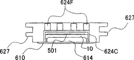
To shown in Figure 8, mounting shell 601 possesses board 610 and cap 620 as Fig. 4.Be housed in electro-optical device 500 in the mounting shell 601 except possessing Fig. 2 and electro-optical device shown in Figure 3, also possess and overlap its lip-deep reflection and prevent other optical elements such as plate, and then flexible connector 501 is connected on its external circuit-connecting terminal.Have, Polarizer or polarizer plate both can possess in the optical system of liquid crystal projector 1100, also can overlap on the surface of electro-optical device 500 again.
In addition, tft array substrate 10 and relative substrate 20 not relative with liquid crystal layer 50 side separately is provided with dustproof with substrate 400 (with reference to Fig. 4 and Fig. 6).Should dustproof constitute in mode with specific thickness with substrate 400.Thus, can prevent to float dust around electro-optical device 500 or dust etc. are attached directly on the surface of this electro-optical device.That is, can eliminate these dusts or dust etc. effectively and amplify the such a bad phenomenon of one-tenth on the image projected.Because the dustproof thickness that has regulation with substrate 400, so it can play because of near the focus that makes light source light and from the position that has this dust or dust, promptly prevent dust and leave the blooming effect that produces with the surface of substrate 400.
Like this, possesses the electro-optical device 500 that tft array substrate 10 and relative substrate 20 and dustproof usefulness substrate 400 etc. are arranged, as shown in Figure 4, be housed in the mounting shell 601 that constitutes by board 610 and cap 620, and between this electro-optical device 500 and mounting shell 601, as Figure 6 and Figure 7, be filled with moulding material 630.Bonding between electro-optical device 500 and the mounting shell 601 can be carried out reliably by this moulding material 630, the generation in the offset of mounting shell 601 inside of electro-optical device 500 can also be done one's utmost to prevent simultaneously.
Having, in this example, is prerequisite with light from cap 620 1 side incidents, through electro-optical device 500, from board 610 1 side outgoing again.In other words, by Fig. 1, relative with colour splitting prism 1112 is not cap 620, but board 610.
In addition, below the board 610 of formation mounting shell 601 and the structure of cap 620 are described in more details.
At first, first, board 610 to shown in Figure 11, is to have the roughly parts of four limit square shapes from viewed in plan as Fig. 4, and relative with the one side of electro-optical device 500 and dispose.In this example, can adopt board 610 directly to contact mutually, be positioned in state on the former as the latter with electro-optical device 500.
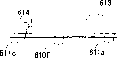
Say that in further detail board 610 has window portion 615, kink 613, intensity reinforcement part 614, cap fixed orifice 612 and mounting hole 611a~611d and 611e.
In addition, the medial surface of kink 613 contacts via the lateral surface of moulding material 630 with electro-optical device 500, thereby can realize the absorption to the former heat from the latter.That is, can make board 610 have function as the heating radiator of electro-optical device 500.Thus, then can prevent effectively owing to strong illumination that 1102 pairs of electro-optical devices in lamp unit 500 carry out causes accumulating of heat in this electro-optical device 500.
In addition, as mentioned above, because the lateral surface of this kink 613 contacts with the medial surface of cap 620, so also can realize from the former person's heat conduction backward.Like this, the absorption owing to the heat that begins from electro-optical device 500 in theory, can proceed to and board 610 and the corresponding degree of the determined thermal capacity of cap 620 both sides, so can carry out the cooling of this electro-optical device 500 extremely effectively.
Cap fixed orifice 612 is the hole portions that are used for being formed at cap 620 protuberance 621 tablings on the relevant position.Board 610 and cap 620 are chimeric mutually and interfixed by this cap fixed orifice 612 and protuberance 621.Have, in this example, this cap fixed orifice 612 is made of two hole portions shown in each figure again.Below, distinguishing under their situation, be called cap fixed orifice 612a and 612b.In addition, therewith accordingly, raised part 621 also is made of two protuberances.Below, distinguishing under their situation, be called protuberance 621a and 621b.
At last, mounting hole 611a~611d is carried out utilization when this being placed electro-optical device in the mounting shell be installed in as shown in Figure 1 the liquid crystal projector 1100.In this example, this mounting hole 611a~611d is set at has the roughly place, four angles of the parts of quadrilateral shape.In addition, in this example, except this mounting hole 611a~611d, also be provided with mounting hole 611e.This mounting hole 611e constitutes leg-of-mutton mode with mounting hole 611c in above-mentioned mounting hole 611a~611d and 611d and disposes.That is, the mode on mounting hole 611e, 611c and the 611d leg-of-mutton to be configured in " each summit " is formed.
Thus, in this example, can adopt 43 fixing and implement to have utilized mounting hole 611e, 611c and 611d fixing two kinds of such fixed forms of the mounting hole 611a~611d that has implemented to utilize four jiaos of places.
And, in this example, especially, have following feature for this board 610.That is, the board 610 of this example, its outermost is black.Here, so-called " outermost " if consider the surface of board 610 is imposed the situation of black coating, then is meant the surface of the coating that adheres to by this coating.In addition, as " outermost " at the position of board 610, specifically be preferably the face of the light exit side that for example comprises board 610, if the face of so-called this light exit side for example by Figure 10 or Figure 11, is meant the represented face with number in the figure 610F.By the way, if by Fig. 9, then the face with not shown paper dorsal part is suitable.
In addition, " outermost " is preferably the face that also comprises the light incident side opposite with it.If it is by Fig. 9, then suitable with the face that is illustrated out.
Like this, because be set as black, can prevent the useless light reflection in this board 610, so can improve image quality by outermost with board 610.For example, as previously mentioned, if the face 610F of light exit side is set as black, then can will passes the window portion 615 and the light that be returned of this board 610 or singly see among light valve 100R, 100G shown in Fig. 1 and the 100B one and from other two outgoing and to the light of this light valve incident etc., owing on above-mentioned board 610, made this useless reflected light be blended into the state of affairs such the projects images, prevent terminating in possible trouble by the face 610F of light exit side reflection by certain element reflects in the liquid crystal projector 1100 as shown in Figure 1.Perhaps, if the face of light incident side is set as black, can prevent that then light from not wishing the situation that takes place to the such basis of this electro-optical device incident from the light exit side of electro-optical device.Thus, can will prevent terminating in possible trouble to the light incident of constructing the TFT on the tft array substrate that constitutes electro-optical device, and both can keep its characteristic well, can avoid again owing to reflected light as described above by electro-optical device etc. again secondary reflection situation that this light finally is blended in the image take place.
As mentioned above,, then can not cause the deterioration of image quality, can show high quality images if adopt this example.
Have again,, can adopt the way of the coating of application black for example or plate other ways or structures such as way as described later with proper metal layers such as nickel, chromium, zinc for the face 610F with above-mentioned light exit side is set as black.
Next, the second, cap 620 to shown in Figure 11, is to have the roughly parts of cube shaped as Fig. 4, and relatively electro-optical device 500 another face and dispose.
These cap 620 preferred resins by light-proofness, metal material etc. constitute, to prevent in the light leak in preventing electro-optical device 500 neighboring areas that parasitic light from entering in the image display area 10a from the neighboring area.In addition, because preferably make this cap 620 have function, so this cap 620 is preferably by the bigger material of heat-conduction coefficient, more specifically say so and be made of aluminium, magnesium, copper or its alloy separately etc. as the heating radiator of board 610 or electro-optical device 500.
In more detail, cap 620 has protuberance 621, lid body 623, cooling air introduction part 622 and cooling air discharge portion 624.At first, protuberance 621 as already as described in, with board 610 fixedly the time be used, and as comprise the structure of two protuberance 612a and 621b and be formed on the corresponding respectively position of above-mentioned cap fixed orifice 612a and 612b on.Have, the protuberance 621 of this example is formed in the mode of the part that constitutes cooling air introduction part 622 or tapered portion 622T described later as shown in Figure 5 again.From the visual angle of Fig. 5,, in Fig. 5, especially it is illustrated though original protuberance 621 can not be illustrated out.
This lid body 623 has window portion 625 and lateral fin sheet portion 627 in more detail.Wherein window portion 625 is that the bottom surface (in Fig. 4 or Fig. 6 etc. for " above ") of above-mentioned box shape is formed opening shape, can make among Fig. 6 from the top part of light transmission downwards.The light that lamp unit 1102 in liquid crystal projector shown in Figure 1 1100 sends can incide in the electro-optical device 500 by this window portion 625.Have again, in lid body 623 with this window portion 625, with similarly, preferably constitute the neighboring area that is positioned at image display area 10a periphery that can make in the electro-optical device 500 and the side edge of window portion 625 and touch the narration of the window portion 615 in the board 610.Like this, can realize the maintenance of electro-optical device 500 by the edge of lid body 623, particularly this window portion 625.In addition, about this point, in this example, especially, with similarly to the narration of the window portion 615 of above-mentioned board 610, on edge to the neighboring area of the window portion 625 of cap 620, also be provided with double-sided belt 2, cap 620 and electro-optical device 500 are by this double-sided belt 2 and by bonding.About this content, narrate afterwards.
On the other hand, lateral fin sheet portion 627 is formed on the two sides of covering body 623.Here so-called two sides are meant the side that does not have cooling air introduction part 622 described later and cooling air discharge portion 624.In more detail, this lateral fin sheet portion 627 is as clear demonstrations such as Fig. 4 or Fig. 6, comprise and show a plurality of from cooling air introduction part 622 to the shape of cooling air discharge portion 624, the part of giving prominence to from above-mentioned side linearlyly (among Fig. 4 etc., each side each and show " two " linearly outstanding part).Thus, the surface area of lid body 623 or cap 620 is increased.
Have, as stating, when cap 620 and board 610 were installed, the lateral surface of the kink 613 in the board 610 can contact (with reference to Fig. 6) with the medial surface of cap 620 again.In this case, so-called above-mentioned " medial surface of cap 620 " is equivalent to cover the medial surface of body 623.
Cooling air introduction part 622 is made of tapered portion 622T and wind deflector 622P as Fig. 4 or Fig. 7 etc. clearly represent.In this example, tapered portion 622T has the profile as its rectangular leg-of-mutton triangular prism in bottom surface substantially.And tapered portion 622T presents an above-mentioned trequetrous side and is attached such profile on a side of lid body 623.In the case, this trequetrous side comprises the limit between the bight that is clamped in the right angle portion on this trequetrous bottom surface and is adjacent.Therefore, tapered portion 622T just becomes the 622T1 of foundation portion with formation maximum height on the side of lid body 623 and has the such shape of leading section 622T2 that begins to reduce highly gradually from it.But said here " highly " is meant the distance of above-below direction among Fig. 7.In Fig. 7,, show the dotted line that extends in the direction as benchmark.On the other hand, one side wind deflector 622P present as on above-mentioned trequetrous bottom surface along the profile of the wall of vertically setting up of two angle clampings except right angle portion.If utilize above-mentioned " highly " to describe, though then the height of tapered portion 622T reduces to above-mentioned leading section 622T2 from the above-mentioned foundation 622T1 of portion, any part of the height of this wind deflector 622P between described foundation 622T1 of portion and leading section 622T2 all is certain.
At last, as Fig. 4, Fig. 5 or Fig. 8 institute clearly expression like that, cooling air discharge portion 624 by flexible connector leading-out portion 624C and afterwards the fin 624F of portion constitute.Wherein, flexible connector leading-out portion 624C is formed on the side relative with the side of the lid body 623 that is formed with above-mentioned tapered portion 622T.More particularly, as shown in Figure 8, present with the cross section be コ word shape parts so that the peristome in this コ word shape cross section in Fig. 8 the below mode be installed in shape such on this side.The flexible connector 501 that is connected on the electro-optical device 500 passes the space that is surrounded by this コ word and is drawn out to the outside.
On the other hand, the back fin 624F of portion is set on for example top board of the above-mentioned コ shaped sections among the flexible connector leading-out portion 624C.This back fin 624F of portion is more specifically as institutes such as Fig. 4, Fig. 5 or Fig. 8 clearly represent, comprise in the corresponding to mode of direction of extending with linearity outshot and show a plurality of (in Fig. 4 etc., and showing " four " linearly outstanding part) shape from the linearly outstanding part of above-mentioned top board as aforesaid lateral fin sheet portion 627.Thus, the surface area of cap 620 is increased.
Because cap 620 forms above such structure, so the wind that the Sirocco fan 1300 that is possessed from liquid crystal projector shown in Figure 1 1100 is sent flows around mounting shell 601 or cap 620 as shown in Figure 12.Here, Figure 12 is the stereographic map that places the electro-optical device in the mounting shell, and being expression places the figure of flow direction of the typical wind of the electro-optical device in the mounting shell to this.Have again, in liquid crystal projector shown in Figure 1 1100, in order to realize the flowing of cooling air as shown in Figure 12, be necessary so that with reference to the relative mode of the cooling air introduction part 622 of illustrated blowing mouth 100RW, the 100GW of Fig. 1 and 100BW and formation cap 620, place electro-optical device in the mounting shell, be light valve 100R, 100G and 100B.
At first, the cooling air ground that can run up as tapered portion 622T, the lid body 623 (with reference to label W1) of blowing over the surface of exposing electro-optical device 500 along cooling air introduction part 622.In addition, owing on cooling air introduction part 622, be provided with wind deflector 622P, so no matter cooling air from which direction, can both be directed to its major part on the tapered portion 622T, and then be directed to and cover (with reference to label W2) on the body 623.Like this,, then wind can be carried to lid body 623 effectively according to this example, except can directly absorb the heat that produces in the electro-optical device 500, promptly directly with its cooling, can also absorb the heat of accumulating in the cap 620 effectively.
In addition, blow to the wind deflector 622P outside of cooling air introduction part 622, the i.e. wind of not relative side with tapered portion 622T, after perhaps as mentioned above near the surface that arrives electro-optical device 500 or its, flow to the wind of the side of covering body 623 etc., will arrive lateral fin sheet portion 627 (with reference to label W3).In this lateral fin sheet portion 627, possess the part that has linearity outstanding as mentioned above, the surface area of lid body 623 is increased, and therefore can realize the effective cooling of this lid body 623 or cap 620.And then, arrive the surface of electro-optical device 500 as described above or near it after, directly lead to the wind etc. of the rear end of cover body 623, will arrive the fin 624F of portion (with reference to label W1) afterwards.In the fin 624F of portion of this back, possessing has the outstanding part of linearity as mentioned above, and the surface area of cooling air discharge portion 624 is increased, and therefore can realize the effective cooling of this cooling air discharge portion 624 or cap 620.
As previously discussed, in a word, the mounting shell 601 of this example can be realized the effective cooling that brought by cooling air.And this situation finally is being diffused into aspect outside very effective according to the heat of the order of electro-optical device 500, board 610 and cap 620 conduction as mentioned above.In addition, so-called cap 620 is cooled off effectively, means can keep effectively all the time from electro-optical device 500 via kink 613 grades to board 610 or flowing to the such heat of cap 620.Promptly, because cap 620 is in the state after being properly cooled under normal conditions, thus function can be kept all the time effectively as heating radiator, therefore, from this cap 620, can carry out from the absorption of the heat of board 610 all the time effectively and then be absorption from the heat of electro-optical device 500.
Thus, the electro-optical device of this example 500 not be because can accumulate heat too much, thus can be with the deterioration of liquid crystal layer 50 or the anti-possible troubles that terminate in such as generation of heat spot, and reduction can cause such worries such as deterioration of image thus extremely effectively.
And, in this example, especially, the function as heating radiator in order to bring into play from this electro-optical device the function that absorbs heat better, promptly to be had as board 610 and cap 620 possesses structure as described below about above-mentioned board 610.That is, in the board 610 of this example, as Fig. 9 or shown in Figure 4, at the edge of window portion 615, be to be provided with the double-sided belt 1 (configuration relation of in Fig. 7, having represented the double-sided belt 1 under the situation that section is observed especially on the part of mounting electro-optical device 500.With reference to part in the circle among the figure).Because the neighboring area that is positioned at image display area 10a periphery in the electro-optical device 500, with the edge contact of this window portion 615, so this electro-optical device 500 and board 610 via this double-sided belt 1 by bonding.
In addition, in this example,, at the edge of the window portion 625 of cap 620 similarly, be provided with double-sided belt 2 as Fig. 5 or shown in Figure 4.Still with reference to part in the above-mentioned circle among Fig. 7.This be because, as described in already, between the neighboring area of the edge of this window portion 625 and electro-optical device 500 preferably also and the relation between board 610 and the electro-optical device 500 similarly, adopt to make it be in contact with one another such structure.Thus, in this example, between cap 620 and the electro-optical device 500 too via double-sided belt 2 by bonding.
Described double-sided belt 1 and 2 whichsoever all has whole edges of surrounding window portion 615 and 625, in other words is the square shape that surrounds the opening portion of this window portion 615 and 625.If it is observed, we can say that then double-sided belt 1 and 2 is provided with accordingly by the whole neighboring area with this electro-optical device 500 from electro-optical device 500 1 sides.
In addition, the double-sided belt 1 and 2 of this example possesses especially and and for example descends feature.That is, the first, double-sided belt 1 and 2 constitutes by having 0.6 (W/mK) or its material above, more preferably 1.0 (W/mK) or its above heat-conduction coefficient.As the double-sided belt that satisfies this condition, specifically can list the band that for example comprises the heat conductivity silicone rubber, adopt and comprise this heat conductivity silicone rubber and simultaneously at adhesive linkage with changed the band etc. of the sandwich construction of its material by adhesive linkage, so can also enumerate as main body comprise ACM, in addition can comprise metal oxide or metal nitride, so-called acrylic acid series heat conductivity double-sided belt etc.Have again, as this double-sided belt, " TCATT heat conductivity binder transfer belt (production code members 9882,9885,9890) " that " the Ehuco TM sheet " that エ Off コ Co., Ltd. (exabyte) manufacturing is arranged that sells on the market or Sumitomo ス リ one エ system Co., Ltd. (exabyte) make etc. utilize them also passable.In addition, the second, described double-sided belt 1 and 2 thickness are set as 50~200 (μ m).
The electro-optical device in the mounting shell of placing at this example that possesses this structure can play following action effect.First, because double-sided belt 1 and 2 have the square shape that surrounds window portion 615 and 625, promptly with the corresponding shape in whole neighboring area of electro-optical device 500, so can in the part of wider scope, carry out double-sided belt 1 and 2 and electro-optical device 500 bonding or bonding with board 610 and cap 620.Therefore, bonding can more reliably and more securely the carrying out between electro-optical device 500 and the board 610 and between electro-optical device 500 and the cap 620 by double-sided belt 1 and 2 with above-mentioned broad area.Especially, when this being placed electro-optical device in the mounting shell be assembled in to wait in the liquid crystal projector 1100, can bigger pulling force arranged effect from the extended flexible connector 501 of electro-optical device as can be known, but in the present invention, owing to have above-mentioned double-sided belt 1 and 2, so even can obtain for above-mentioned bigger pulling force, also can not cause easily the such advantage of offset of the electro-optical device 500 in the mounting shell 601.
The second, because double-sided belt 1 and 2 is made of the material with high heat-conduction coefficient as described above, so can carry out effectively from electro-optical device 500 to the heat conduction of board 610 or from of the heat conduction of this device 500 to cap 620.
And, double-sided belt 1 and 2, owing to have square shape as mentioned above and have the area of broad, in addition, also because the thickness of this double-sided belt 1 and 2 is set as 50~200 (μ m), so can further promote above-mentioned heat conducting action effect.
At first, according to the former " square shape ", because electro-optical device 500 and double-sided belt 1 or 2 or board 610 and double-sided belt 1 and then cap 620 and double-sided belt 2 contact in wide region respectively, so can carry out above-mentioned heat conduction more effectively.
In addition, according to the restriction of the thickness of the latter's double-sided belt 1 and 2, then can carry out effectively from electro-optical device 500 to the heat conduction of board 610 or from of the heat conduction of this device 500 according to the following fact to cap 620.Below, be explained with reference to Figure 13 and Figure 14.Here, Figure 13 is the variation in thickness of representing qualitatively along with double-sided belt 1 or 2, how to change from the heat conduction efficiency of electro-optical device 500, perhaps the curve map how to change of the position offset of this electro-optical device 500 in mounting shell 601 to board 610 or cap 620.In addition, Figure 14 is the partial enlarged drawing of the interior part of circle of the lower left in the interior part of four circles among Fig. 7, (a) the smaller situation (being lower than the situation of 50 (μ m)) of thickness of expression double-sided belt, (b) situation that the thickness of expression double-sided belt is bigger (situation that surpasses 200 (μ m)).
Have again, between the thickness of double-sided belt 1 and above-mentioned heat conduction efficiency or position offset, usually can see relation as shown in figure 13, but one of main as its reason, can be set forth on the surface of board 610 and have random concavo-convex 610S as shown in figure 14.Here so-called concavo-convex 610S be meant can be by constituting board 610 material the very trickle shape that shows of intrinsic surfaceness.Have, relative therewith, usually the dustproof surface accuracy with substrate 400 that is made of quartz glass etc. is extremely good, as shown in figure 14, if come comparison according to the difference of height of the concavo-convex 610S that is seen on the plane of board 610, then almost is quite smooth again.
With this concavo-convex 610S is prerequisite, if the thickness of hypothesis double-sided belt 1 is lower than the situation of 50 (μ m), be reason then, form, can not make its whole with dustproof bonding with substrate 400 just like the part of this double-sided belt 1 is buried the such state of recess in above-mentioned concavo-convex 610S with this concavo-convex 610S.Say it on the contrary, shown in the label P of Figure 14 (a), dustproof only formed the form that the summit with for example protuberance contacts with substrate 400 and double-sided belt 1.Therefore, the bonding force of the two dies down, the position offset of the electro-optical device 500 in the mounting shell 601 become big (with reference to the dotted line among Figure 13).In addition, in this case, because identical, can produce with above-mentioned concavo-convex 610S between preventing dust with substrate 400 and board 610 be the gap V that reason is brought, so the heat conduction efficiency of the two also reduces.Therefore, reduce from the conduction of electro-optical device 500 to the heat of board 610.
On the other hand, if the thickness of hypothesis double-sided belt surpasses the situation of 200 (μ m), then because this thickness filled up the difference of height of above-mentioned concavo-convex 610S and residue arranged, so can carry out bonding between board 610 and the double-sided belt 1 and dustproof bonding with between substrate 400 and the double-sided belt 1 respectively effectively.But, in this case, because in the elastic force that can produce in the double-sided belt 1 shown in the label F of Figure 14 (b), so just might produce board 610 and dustproof with the relative offset (with reference to the dotted line among Figure 14 (b)) between the substrate 400.The amount of this offset can be thought according to the thickness of double-sided belt 1 and dull increase (with reference to the dotted line among Figure 13).In addition, because the big more distance that then is used to conduct heat of the thickness of double-sided belt 1 is just long more, so heat conduction efficiency can reduce (with reference to the dotted line among Figure 13) as can be known.
Have, Figure 14 for convenience of explanation, express as the inner partial enlarged drawing that divides of the circumference of the lower-left in the part in four circles among Fig. 7 as mentioned above, but the obvious fact as described above can be described as same for part in all four circles among Fig. 7 again.
According to above such fact and as the curve map shown in Figure 13, the thickness of the double-sided belt 1 of this example (perhaps 2) is 50~200 (μ m), we can say forming bonding between board 610 (perhaps cap 620) and the electro-optical device 500 more reliably and realizing from the latter to being best aspect the former the good heat conduction.
Have again, because the relation of the thickness of double-sided belt 1 among Figure 14 or 2 and above-mentioned heat conduction efficiency or position offset of considering is the main cause that exists for concavo-convex 610S as mentioned above, so in other words according to the size of board 610 or cap 620 outmost surfacenesses how according to the size of this concavo-convex 610S,, double-sided belt 1 or 2 thickness can change aptly.That is, also can produce following situation, if above-mentioned surfaceness is little, even then use thinner double-sided belt 1 or 2 also can not produce above-mentioned undesirable condition, in addition, if above-mentioned roughness is big, then thicker double-sided belt 1 or 2 is more suitable.
This is the part of the core when preferably stipulating " double-sided belt " should have among the present invention thickness.The qualification of above-mentioned so-called 50~200 (μ m), as proposing with the common conceivable corresponding optimum value of concavo-convex 610S difference of height, but it is according to circumstances different, as mentioned above, also can adjust above-mentioned thickness according to the size of above-mentioned surfaceness, and then, even the situation that surpasses above-mentioned numerical range because of this adjustment also has no relations.This situation is also contained in the scope of the present invention.
By the above, in a word, can be more reliably and carry out the fixing of electro-optical device 500 and board 610 and cap 620 more effectively, in addition, can carry out person's heat conduction backward effectively from the former.Therefore, can prevent from mounting shell 601, to cause the situation of electro-optical device 500 offsets with doing one's utmost, in addition, because can also realize the cooling of this electro-optical device 500 effectively, so can not cause with the deterioration of liquid crystal be the image quality deterioration of reason.
Have again, board 610 for above-mentioned example, as described in already, implemented to make its outermost to present the such processing of black, if but according to the relation of this point and above-mentioned double-sided belt 1, adopt following structure, then enjoy more effectively aspect the action effect of the present invention even more ideal.
That is, be made as black for the outermost with board 610 this moment, preferably adopts the method (following is representative with plating Ni) of the coating processing of implementing nickel, cobalt, zinc etc. after the surface to this board 610 imposes blasting treatment, again.If like this, at first, because this blasting treatment, on the surface of board 610, can form random concavo-convexly and be bigger concavo-convex (with reference to Figure 14 (a) and (b)) usually, prevent effect so can more effectively enjoy above-mentioned light reflection.In addition, handle, then compare, can make the bonding force between board 610 and the double-sided belt 1 stronger with the situation that obtains black by the coating processing if applied plating Ni.If utilize coating to handle, then be easy between the surface of coating and board 610, produce and peel off.In this example,,, thus, can realize bonding between board 610 and the electro-optical device 500 more reliable and more firmly so board 610 and double-sided belt 1 can be by more reliable and bonding more firmly because can not produce this undesirable condition.
By the way, in above-mentioned example, though the outermost that makes cap 620 being presented the situation of black does not describe especially, but too for this cap 620, in order as already illustrating, to prevent the exposure in electro-optical device 500 neighboring areas and to prevent that simultaneously parasitic light from entering in the image display area 10a from the neighboring area, preferably makes it have light-proofness.Therefore, in the present invention, preferably to this cap 620 also with above-mentioned board 610 similarly, impose coating processing, coating processing etc. and make its outermost become the processing of black.In this case, also to be careful the relation between cap 620 and the double-sided belt 2, to the narration of board 610,, preferably adopt surface to this cap 620 to impose the method that blasting treatment and plating Ni handle too as above for the outermost with this cap 620 is made as black.
In addition, in above-mentioned example, though the shape of double-sided belt 1 or 2 is set to the square shape that surrounds window portion 615 or 625, the present invention is not limited to such form formula.Also can adopt for example Figure 15 and form shown in Figure 16.Here, Figure 15 and Figure 16 are the figures identical with Fig. 9 purport, are expressions and the figure of this figure different form of its shape when seeing double-sided belt on the plane.Having, below is that representative describes with the double-sided belt relevant with board 610 again.
At first, in Figure 15, only formed the form that on the part of above-below direction in the figure of window portion 615, is provided with double-sided belt 11.This double-sided belt 11 we can say for example have strip.Have again, replace the form of Figure 15, only also can adopt the form that on the part of left and right directions in the figure of window portion 615, is provided with double-sided belt.In addition, in Figure 16, only formed and to be provided with the form of double-sided belt 12 with four jiaos of corresponding parts of window portion 615., in this example,, had better not make its area too small for each double-sided belt 12.Because if make the area of double-sided belt 12 too small and form the state of " spot gluing ", then can't keep bonding between board 610 and the electro-optical device 500 well.Therewith accordingly, double-sided belt of the present invention preferably has the above area of setting, thus, preferably adopts the such form of 500 one-tenth of board 610 and electro-optical devices " face is bonding ".Have again, which type of form is that " spot gluing " which type of form is " face is bonding ", will be with the size of this electro-optical device 500, specifically be tft array substrate 10, how or the like substrate 20 and the dustproof size or the surface accuracy of the size of the size of board 610 and then above-mentioned concavo-convex 610S and even board 610 with substrate 400, particularly above-mentioned neighboring area be principal element relatively, determines to design item.
In so various deformation forms, compare with Fig. 9 etc., because can control the amount of employed double-sided belt, so can realize the reduction of the cost of this part.Have, above-described deformation form also can fully similarly be suitable for cap 620 even can think again.
And then, in above-mentioned example, though bonding between bonding and electro-optical device 500 between electro-optical device 500 and the board 610 and the cap 620 realizes that by double-sided belt 1 and 2 the present invention is not limited to this form.For example, also can be in the circle of Fig. 7 the double-sided belt 1 shown in part or Fig. 4, Fig. 9 etc. and 2 the position is set, replace this double-sided belt 1 and 2 and be provided with by silicone resin etc. constitute as the moulding material of bonding agent, silicone RTV rubber etc. specifically.
The invention is not restricted to above-mentioned example, can in the scope of the main idea of not violating accessory rights requirement and intelligible invention from instructions integral body or thought, suitably change, follow place the electro-optical device and the projection type image display apparatus in the mounting shell of this change also to be included in the technical scope of the present invention.As electro-optical device, except liquid crystal panel, also applicable to electrophoretic apparatus, electroluminescence device, plasm display device and used Field Emission Display and the device of electron-emitting device such as Surface-Conduction Electron-Emitter Display etc.
Claims (10)
1. one kind places the electro-optical device in the mounting shell, it is characterized in that possessing:
The electro-optical device that projection light is arranged from light source incident on image display area; And
Be made up of with the lid that covers above-mentioned electro-optical device and have a position that contacts with above-mentioned plate the plate that relatively disposes with the one side of this electro-optical device, at least a portion of neighboring area that keeps the periphery that is arranged in above-mentioned image display area in the above-mentioned electro-optical device is to take in the mounting shell of this electro-optical device;
The surface of above-mentioned plate is subjected to coating and handles after being subjected to blasting treatment;
Above-mentioned plate has and the above-mentioned image display area of the above-mentioned electro-optical device window portion of opening accordingly;
Neighboring area in the above-mentioned window portion of the face relative of above-mentioned plate with above-mentioned electro-optical device, via double-sided belt that above-mentioned plate is mutually bonding with above-mentioned electro-optical device.
2. the electro-optical device that places in the mounting shell according to claim 1 is characterized in that only having above-mentioned double-sided belt on four jiaos zone of above-mentioned neighboring area.
3. the electro-optical device that places in the mounting shell according to claim 1 is characterized in that, has above-mentioned double-sided belt in above-mentioned neighboring area on the zone at the edge on opposed facing 2 limits.
4. the electro-optical device that places in the mounting shell according to claim 1 is characterized in that above-mentioned double-sided belt comprises ACM.
5. the electro-optical device that places in the mounting shell according to claim 1 is characterized in that, above-mentioned double-sided belt is made of the material with 0.6 (W/mK) or its above heat-conduction coefficient.
6. according to any described electro-optical device that places in the mounting shell in the claim 1~5, it is characterized in that outmost at least one side of the outermost of above-mentioned plate and above-mentioned lid is black.
7. the electro-optical device that places in the mounting shell according to claim 6 is characterized in that, the surface of above-mentioned lid is imposed coating handle.
8. the electro-optical device that places in the mounting shell according to claim 7 is characterized in that above-mentioned coating is handled and implemented again after the surface to above-mentioned lid imposes blasting treatment.
9. one kind places the electro-optical device in the mounting shell, it is characterized in that possessing:
The electro-optical device that projection light is arranged from light source incident on image display area; And
Be made up of with the lid that covers above-mentioned electro-optical device and have a position that contacts with above-mentioned plate the plate that relatively disposes with the one side of this electro-optical device, at least a portion of neighboring area that keeps the periphery that is arranged in above-mentioned image display area in the above-mentioned electro-optical device is to take in the mounting shell of this electro-optical device;
Above-mentioned plate has and the above-mentioned image display area of the above-mentioned electro-optical device window portion of opening accordingly, handles and makes its blackization by the surface sequentially being imposed blasting treatment and coating;
In the neighboring area of the above-mentioned window portion of the face relative with above-mentioned electro-optical device of above-mentioned plate, via the double-sided belt of 50~200 micron thickness, the surface that blasting treatment that being subjected to of above-mentioned plate is above-mentioned and coating are handled is mutually bonding with above-mentioned electro-optical device.
10. a projection type image display apparatus is characterized in that, possessing has:
Any described electro-optical device that places in the mounting shell in the claim 1 to 9;
Above-mentioned light source;
With the lead optical system of above-mentioned electro-optical device of above-mentioned projection light; And
Projection is from the projection optics system of the projection light of above-mentioned electro-optical device outgoing.
Applications Claiming Priority (2)
| Application Number | Priority Date | Filing Date | Title |
|---|---|---|---|
| JP2002370070A JP3707470B2 (en) | 2002-12-20 | 2002-12-20 | ELECTRO-OPTICAL DEVICE WITH MOUNTING CASE AND PROJECTION TYPE DISPLAY DEVICE |
| JP370070/2002 | 2002-12-20 |
Publications (2)
| Publication Number | Publication Date |
|---|---|
| CN1510473A CN1510473A (en) | 2004-07-07 |
| CN1296755C true CN1296755C (en) | 2007-01-24 |
Family
ID=32766112
Family Applications (1)
| Application Number | Title | Priority Date | Filing Date |
|---|---|---|---|
| CNB2003101218208A Expired - Fee Related CN1296755C (en) | 2002-12-20 | 2003-12-19 | Electro-optical device in installing shell and projecting displaying device |
Country Status (5)
| Country | Link |
|---|---|
| US (1) | US7289172B2 (en) |
| JP (1) | JP3707470B2 (en) |
| KR (1) | KR20040055658A (en) |
| CN (1) | CN1296755C (en) |
| TW (1) | TWI231461B (en) |
Families Citing this family (11)
| Publication number | Priority date | Publication date | Assignee | Title |
|---|---|---|---|---|
| JP4508214B2 (en) * | 2007-05-23 | 2010-07-21 | ソニー株式会社 | Display device |
| CN101788751B (en) * | 2009-01-23 | 2013-03-27 | 上海三鑫科技发展有限公司 | Optical engine for mini projector |
| JP5487704B2 (en) * | 2009-04-27 | 2014-05-07 | セイコーエプソン株式会社 | Electro-optical device and electronic apparatus |
| JP5533001B2 (en) * | 2010-02-16 | 2014-06-25 | セイコーエプソン株式会社 | Electro-optical device and electronic apparatus |
| TWI477882B (en) * | 2012-05-04 | 2015-03-21 | Young Optics Inc | Projection device and light valve module thereof |
| TWI550333B (en) * | 2012-05-04 | 2016-09-21 | 揚明光學股份有限公司 | Projection device and light valve module thereof |
| JP6236781B2 (en) * | 2012-12-28 | 2017-11-29 | 株式会社リコー | Light tunnel and image irradiation device |
| US9684197B2 (en) * | 2013-12-10 | 2017-06-20 | Seiko Epson Corporation | Electro-optic device and electronic apparatus |
| JP6604745B2 (en) * | 2015-05-15 | 2019-11-13 | キヤノン株式会社 | Light modulation element unit and image projection apparatus |
| CN105182669B (en) * | 2015-09-25 | 2017-05-31 | 苏州佳世达光电有限公司 | Ray machine module |
| JP6361939B2 (en) * | 2016-03-08 | 2018-07-25 | パナソニックIpマネジメント株式会社 | Display device |
Citations (5)
| Publication number | Priority date | Publication date | Assignee | Title |
|---|---|---|---|---|
| JPH10133590A (en) * | 1996-10-28 | 1998-05-22 | Nitto Denko Corp | Light emission display device |
| JPH10254366A (en) * | 1997-03-17 | 1998-09-25 | Sony Corp | Liquid crystal display device |
| US5835179A (en) * | 1996-08-30 | 1998-11-10 | Sony Corporation | Liquid crystal display |
| CN2381023Y (en) * | 1998-12-16 | 2000-05-31 | 北方专业设计工艺局“Nord” | Thermoelectric cooler |
| JP2002107698A (en) * | 2000-09-29 | 2002-04-10 | Sharp Corp | Display element and projection liquid crystal display device |
Family Cites Families (11)
| Publication number | Priority date | Publication date | Assignee | Title |
|---|---|---|---|---|
| JPS6170247U (en) * | 1984-10-05 | 1986-05-14 | ||
| JPH05324562A (en) | 1992-05-26 | 1993-12-07 | Matsushita Electric Ind Co Ltd | Electronic equipment device |
| JPH10171368A (en) * | 1996-12-09 | 1998-06-26 | Sony Corp | Image display device |
| WO1998036313A1 (en) | 1997-02-12 | 1998-08-20 | Hitachi, Ltd. | Liquid crystal display |
| JPH10232629A (en) | 1997-02-20 | 1998-09-02 | Sony Corp | Liquid crystal display element and projection type liquid crystal display device formed by using the same |
| JP3296993B2 (en) * | 1997-04-08 | 2002-07-02 | エルジー フィリップス エルシーディー カンパニー リミテッド | Portable computer with liquid crystal display |
| JP2001318361A (en) | 2000-05-11 | 2001-11-16 | Seiko Epson Corp | Optical modulating device and projector using the same |
| JP2002244214A (en) | 2001-02-20 | 2002-08-30 | Seiko Epson Corp | Projector |
| KR100840715B1 (en) * | 2002-05-28 | 2008-06-23 | 삼성전자주식회사 | Back light assembly and liquid crystal display having the same |
| JP2004045680A (en) | 2002-07-11 | 2004-02-12 | Sony Corp | Liquid crystal display device and projector |
| JP3736522B2 (en) * | 2002-12-20 | 2006-01-18 | セイコーエプソン株式会社 | ELECTRO-OPTICAL DEVICE WITH MOUNTING CASE, PROJECTION TYPE DISPLAY DEVICE, AND MOUNTING CASE |
-
2002
- 2002-12-20 JP JP2002370070A patent/JP3707470B2/en not_active Expired - Fee Related
-
2003
- 2003-12-03 US US10/725,424 patent/US7289172B2/en not_active Expired - Fee Related
- 2003-12-12 TW TW092135257A patent/TWI231461B/en not_active IP Right Cessation
- 2003-12-18 KR KR1020030093251A patent/KR20040055658A/en active Search and Examination
- 2003-12-19 CN CNB2003101218208A patent/CN1296755C/en not_active Expired - Fee Related
Patent Citations (5)
| Publication number | Priority date | Publication date | Assignee | Title |
|---|---|---|---|---|
| US5835179A (en) * | 1996-08-30 | 1998-11-10 | Sony Corporation | Liquid crystal display |
| JPH10133590A (en) * | 1996-10-28 | 1998-05-22 | Nitto Denko Corp | Light emission display device |
| JPH10254366A (en) * | 1997-03-17 | 1998-09-25 | Sony Corp | Liquid crystal display device |
| CN2381023Y (en) * | 1998-12-16 | 2000-05-31 | 北方专业设计工艺局“Nord” | Thermoelectric cooler |
| JP2002107698A (en) * | 2000-09-29 | 2002-04-10 | Sharp Corp | Display element and projection liquid crystal display device |
Also Published As
| Publication number | Publication date |
|---|---|
| US20040160548A1 (en) | 2004-08-19 |
| CN1510473A (en) | 2004-07-07 |
| US7289172B2 (en) | 2007-10-30 |
| TW200424972A (en) | 2004-11-16 |
| KR20040055658A (en) | 2004-06-26 |
| JP2004198935A (en) | 2004-07-15 |
| JP3707470B2 (en) | 2005-10-19 |
| TWI231461B (en) | 2005-04-21 |
Similar Documents
| Publication | Publication Date | Title |
|---|---|---|
| CN1196088C (en) | Liquid crystal panel and method for producing the same, and projection display device | |
| CN1232862C (en) | Electro-optic device with sealed case, projecting displaying device, sealed case and manufacturing method thereof | |
| CN1295550C (en) | Mulberry laminar, casing and module for display panel and cooling method thereof | |
| CN1267774C (en) | Optical modulator, optical apparatus anjd projector | |
| CN1287196C (en) | Electro-optical device in installing shell, projecting displaying device and installing shell | |
| CN1313868C (en) | Electro-optical device in installing shell, projecting displaying device and installing shell | |
| CN1296754C (en) | Electro-optical device in installing shell, projecting displaying device and installing shell | |
| CN1296755C (en) | Electro-optical device in installing shell and projecting displaying device | |
| CN1790112A (en) | Mounting case for electro-optical device, method of manufacturing mounting case for electro-optical device, electro-optical device, and electronic apparatus | |
| CN1658064A (en) | Optical device and projector | |
| CN1308751C (en) | Photoelectric device fitting with mounting shell and projection type displaying device | |
| JP3711987B2 (en) | ELECTRO-OPTICAL DEVICE WITH MOUNTING CASE, PROJECTION TYPE DISPLAY DEVICE, AND MOUNTING CASE | |
| CN1301439C (en) | Electrooptical apparatus in case projective display and mounting case | |
| JP5287119B2 (en) | Electro-optical device and electronic apparatus | |
| CN1721926A (en) | Electro-optical device, method of manufacturing the same, and electronic apparatus using electro-optical device | |
| CN1540424A (en) | Electrooptical device with mounting casting and projecting displaying device and mounting casting | |
| CN1540425A (en) | Electrooptical device with mounting casing and projecting displaying device and mounting casing | |
| JP4385598B2 (en) | ELECTRO-OPTICAL DEVICE WITH MOUNTING CASE, PROJECTION TYPE DISPLAY DEVICE, AND MOUNTING CASE | |
| JP4215029B2 (en) | ELECTRO-OPTICAL DEVICE WITH MOUNTING CASE, PROJECTION TYPE DISPLAY DEVICE, AND MOUNTING CASE | |
| JP4378945B2 (en) | ELECTRO-OPTICAL DEVICE WITH MOUNTING CASE, PROJECTION TYPE DISPLAY DEVICE, AND MOUNTING CASE | |
| JP4168801B2 (en) | ELECTRO-OPTICAL DEVICE WITH MOUNTING CASE, PROJECTION TYPE DISPLAY DEVICE, AND MOUNTING CASE | |
| JP5332482B2 (en) | Electro-optical device and electronic apparatus |
Legal Events
| Date | Code | Title | Description |
|---|---|---|---|
| C06 | Publication | ||
| PB01 | Publication | ||
| C10 | Entry into substantive examination | ||
| SE01 | Entry into force of request for substantive examination | ||
| C14 | Grant of patent or utility model | ||
| GR01 | Patent grant | ||
| C17 | Cessation of patent right | ||
| CF01 | Termination of patent right due to non-payment of annual fee |
Granted publication date: 20070124 Termination date: 20121219 |