CN1196088C - Liquid crystal panel and method for producing the same, and projection display device - Google Patents
Liquid crystal panel and method for producing the same, and projection display device Download PDFInfo
- Publication number
- CN1196088C CN1196088C CNB981192076A CN98119207A CN1196088C CN 1196088 C CN1196088 C CN 1196088C CN B981192076 A CNB981192076 A CN B981192076A CN 98119207 A CN98119207 A CN 98119207A CN 1196088 C CN1196088 C CN 1196088C
- Authority
- CN
- China
- Prior art keywords
- transparency carrier
- electro
- substrate
- optical device
- optical
- Prior art date
- Legal status (The legal status is an assumption and is not a legal conclusion. Google has not performed a legal analysis and makes no representation as to the accuracy of the status listed.)
- Expired - Lifetime
Links
Images


Classifications
-
- G—PHYSICS
- G02—OPTICS
- G02F—OPTICAL DEVICES OR ARRANGEMENTS FOR THE CONTROL OF LIGHT BY MODIFICATION OF THE OPTICAL PROPERTIES OF THE MEDIA OF THE ELEMENTS INVOLVED THEREIN; NON-LINEAR OPTICS; FREQUENCY-CHANGING OF LIGHT; OPTICAL LOGIC ELEMENTS; OPTICAL ANALOGUE/DIGITAL CONVERTERS
- G02F1/00—Devices or arrangements for the control of the intensity, colour, phase, polarisation or direction of light arriving from an independent light source, e.g. switching, gating or modulating; Non-linear optics
- G02F1/01—Devices or arrangements for the control of the intensity, colour, phase, polarisation or direction of light arriving from an independent light source, e.g. switching, gating or modulating; Non-linear optics for the control of the intensity, phase, polarisation or colour
- G02F1/13—Devices or arrangements for the control of the intensity, colour, phase, polarisation or direction of light arriving from an independent light source, e.g. switching, gating or modulating; Non-linear optics for the control of the intensity, phase, polarisation or colour based on liquid crystals, e.g. single liquid crystal display cells
- G02F1/133—Constructional arrangements; Operation of liquid crystal cells; Circuit arrangements
- G02F1/1333—Constructional arrangements; Manufacturing methods
- G02F1/133308—Support structures for LCD panels, e.g. frames or bezels
-
- G—PHYSICS
- G02—OPTICS
- G02F—OPTICAL DEVICES OR ARRANGEMENTS FOR THE CONTROL OF LIGHT BY MODIFICATION OF THE OPTICAL PROPERTIES OF THE MEDIA OF THE ELEMENTS INVOLVED THEREIN; NON-LINEAR OPTICS; FREQUENCY-CHANGING OF LIGHT; OPTICAL LOGIC ELEMENTS; OPTICAL ANALOGUE/DIGITAL CONVERTERS
- G02F1/00—Devices or arrangements for the control of the intensity, colour, phase, polarisation or direction of light arriving from an independent light source, e.g. switching, gating or modulating; Non-linear optics
- G02F1/01—Devices or arrangements for the control of the intensity, colour, phase, polarisation or direction of light arriving from an independent light source, e.g. switching, gating or modulating; Non-linear optics for the control of the intensity, phase, polarisation or colour
- G02F1/13—Devices or arrangements for the control of the intensity, colour, phase, polarisation or direction of light arriving from an independent light source, e.g. switching, gating or modulating; Non-linear optics for the control of the intensity, phase, polarisation or colour based on liquid crystals, e.g. single liquid crystal display cells
- G02F1/133—Constructional arrangements; Operation of liquid crystal cells; Circuit arrangements
- G02F1/1333—Constructional arrangements; Manufacturing methods
- G02F1/1335—Structural association of cells with optical devices, e.g. polarisers or reflectors
- G02F1/133509—Filters, e.g. light shielding masks
- G02F1/133512—Light shielding layers, e.g. black matrix
-
- H—ELECTRICITY
- H04—ELECTRIC COMMUNICATION TECHNIQUE
- H04N—PICTORIAL COMMUNICATION, e.g. TELEVISION
- H04N9/00—Details of colour television systems
- H04N9/12—Picture reproducers
- H04N9/31—Projection devices for colour picture display, e.g. using electronic spatial light modulators [ESLM]
- H04N9/3102—Projection devices for colour picture display, e.g. using electronic spatial light modulators [ESLM] using two-dimensional electronic spatial light modulators
- H04N9/3105—Projection devices for colour picture display, e.g. using electronic spatial light modulators [ESLM] using two-dimensional electronic spatial light modulators for displaying all colours simultaneously, e.g. by using two or more electronic spatial light modulators
-
- G—PHYSICS
- G02—OPTICS
- G02F—OPTICAL DEVICES OR ARRANGEMENTS FOR THE CONTROL OF LIGHT BY MODIFICATION OF THE OPTICAL PROPERTIES OF THE MEDIA OF THE ELEMENTS INVOLVED THEREIN; NON-LINEAR OPTICS; FREQUENCY-CHANGING OF LIGHT; OPTICAL LOGIC ELEMENTS; OPTICAL ANALOGUE/DIGITAL CONVERTERS
- G02F1/00—Devices or arrangements for the control of the intensity, colour, phase, polarisation or direction of light arriving from an independent light source, e.g. switching, gating or modulating; Non-linear optics
- G02F1/01—Devices or arrangements for the control of the intensity, colour, phase, polarisation or direction of light arriving from an independent light source, e.g. switching, gating or modulating; Non-linear optics for the control of the intensity, phase, polarisation or colour
- G02F1/13—Devices or arrangements for the control of the intensity, colour, phase, polarisation or direction of light arriving from an independent light source, e.g. switching, gating or modulating; Non-linear optics for the control of the intensity, phase, polarisation or colour based on liquid crystals, e.g. single liquid crystal display cells
- G02F1/133—Constructional arrangements; Operation of liquid crystal cells; Circuit arrangements
- G02F1/1333—Constructional arrangements; Manufacturing methods
- G02F1/133388—Constructional arrangements; Manufacturing methods with constructional differences between the display region and the peripheral region
-
- G—PHYSICS
- G02—OPTICS
- G02F—OPTICAL DEVICES OR ARRANGEMENTS FOR THE CONTROL OF LIGHT BY MODIFICATION OF THE OPTICAL PROPERTIES OF THE MEDIA OF THE ELEMENTS INVOLVED THEREIN; NON-LINEAR OPTICS; FREQUENCY-CHANGING OF LIGHT; OPTICAL LOGIC ELEMENTS; OPTICAL ANALOGUE/DIGITAL CONVERTERS
- G02F2201/00—Constructional arrangements not provided for in groups G02F1/00 - G02F7/00
- G02F2201/46—Fixing elements
- G02F2201/465—Snap -fit
Abstract
The present invention is an electro-optical device, projection display device and production thereof. In the liquid crystal device 30 of the present invention, since a third transparent substrate 600 is adhered by a transparent adhesive agent 91 on an outer surface 302 of an active matrix substrate 300, no flaw or no dust is adhered to the outer surface 302 of the active matrix substrate 300. Besides, even if the flaw or dust is adhered to the outer surface 922 of the third transparent substrate, this kind of flaw or dust is not projected onto the projected picture. Also, the designed boundary of mask body 900 can be enlarged according to the condition of forming the light-shielding film on the third transparent substrate.
Description
Technical field
The present invention relates to a kind of electro-optical device, use the projecting display of this electro-optical device, and the method for making this electro-optical device.More specifically say, the present invention relates to be provided with the constructing technology of electrooptical material, its outside surface side in the inboard of two plate bases, and the formation technology that should construct.
Background technology
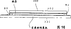
As shown in figure 16, electro-optical device mainly by the active-matrix substrate 300 that is formed with pixel capacitors and pixel switch element (first transparency carrier), be formed with the counter substrate 400 (second transparency carrier) of opposite electrode and be arranged on active-matrix substrate 300 and counter substrate 400 between constitute as the liquid crystal LC of electrooptical material one example.Liquid crystal LC be filled between active-matrix substrate 300 and the counter substrate 400 and the zone that separates with sealant 80 in, control liquid crystal aligning between active-matrix substrate 300 and the counter substrate 400 by each pixel.
Therefore, the electro-optical device that will have above-mentioned structure therein is as in projection-type liquid crystal's device of light valve, from the light of light emitted by light-gathering optics optically focused, and with its guiding electro-optical device, after with electro-optical device this light being carried out optical modulation, by the enlarging projection optical system with required image projection on projecting plane such as screen.
Though be installed in usually in the light shield shell that is provided with the viewing area corresponding opening by the electro-optical device of above-mentioned formation, the frame of viewing area (profile) is normally limited by the optical screen film made from Cr (chromium) and similar substance on counter substrate 400 (hereinafter referred to as separating contour).In other words, because the end of the opening of the shell of being made by plastics and similar substance is difficult to have enough dimensional accuracies because of there is burr in edge, therefore the design margin at the shell aperture place is that width by the separation contour guarantees.According to this technology, when with from the top view viewing area, when falling into the opening of the precision formation shell in the width range of separating contour with the end that makes shell aperture as far as possible, can avoid the viewing area to be hidden in the shell aperture back, or see the problem of plate portion of the outside, viewing area of the periphery avris of separating contour from opening portion.
Yet, in existing electro-optical device, when when the angle of liquid crystal LC is observed, because the outside surface 302 of active- matrix substrate 300 or 402 thickness of outside surface of counter substrate electrode 400 by these transparency carriers, for example 1mm divides right and left, and focuses on light on the liquid crystal LC and also focuses on simultaneously on the scar and dust on the outside surface that is attached to these transparency carriers.Therefore, resemble 10 μ m little scar and dust to the 20 μ m and just be presented in the projection image, thereby reduced image quality.
In projection-type liquid crystal's device, because there is high light to shine on the electro-optical device, thereby make the thickness attenuation of active-matrix substrate 300 and counter substrate 400 from light source, cause that easily local temperature raises.The part that is locally heated like this has different transmissivities with the peripheral region, therefore image quality is degenerated.In addition, this temperature rising also is the reason of liquid crystal LC deterioration.
Open in flat 9-105901 communique and the flat 9-113906 communique of Te Kai the spy and to have proposed a kind of structure as shown in figure 17, wherein use grafting material 101 that transparency carrier 102 is fixed on the outside surface 302 of active-matrix substrate 300 through air layer (air), thereby by carry out the temperature rising that heat radiation has suppressed electro-optical device from this transparency carrier 102, and, prevented from the outside surface 302 of active-matrix substrate 300, to adhere to scar and dust because this transparency carrier 102 is arranged.Yet, in having the electro-optical device of constructing as shown in figure 17, because the cause of relative transparency carrier 102 is set through air layer (air) on the outside surface 302 of active-matrix substrate 300, be increased between active-matrix substrate 300 and the air layer and the interface between air layer (air) and the transparency carrier 102 and be new reflecting interface, increased reflection at the interface thus.Therefore, in the electro-optical device of constructing as shown in figure 17, increased the loss of luminous energy, thereby caused the new problem of projection image deepening.Although can be designed to vacuum moulding machine antireflection film on the inside surface 104 of the outside surface 302 of active-matrix substrate 300 and transparency carrier 102, form this antireflection film unusual effort in vacuum environment, cause the production cost of electro-optical device to increase greatly.Can't prevent that dust is attached on the outside surface 302 of active-matrix substrate 300 in that transparency carrier 102 only is set on the outside surface 302 of active-matrix substrate 300, therefore can not avoid the deterioration of displayed image quality fully.
In described conventional electro-optical device so far, existence can not improve dust reduction capability simultaneously with low manufacturing cost and good balance, defocus first problem of function and thermal radiation function.
On the other hand, in current electro-optical device field, to doing plate again little and good demand or guarantee that in limited plate face the requirement of big viewing area is strong, this has strengthened the necessity of the narrowed width that makes the separation contour that is provided with at the counter substrate place as mentioned above.Particularly, since the sealing area that engages two substrates with bonding agent be present in separate contour near, thereby when adhering to two substrates,, also require to separate the narrowed width of contour in order not block ultraviolet ray irradiation from outer surface of substrate with the bonding agent that comprises ultraviolet curing resin.Occurred second problem thus, promptly according to adopting above-mentioned separation contour to guarantee the technology of the design margin of shell aperture part, along with the narrowed width of separating contour, the design margin of shell aperture part reduces.
In addition, another problem has appearred, promptly when the electro-optical device that has such separation contour is used to projector projecting displays such as (projector) and uses the transmission-type display device of grade backlight, particularly when separating the narrowed width of contour, according to the angle of incident light and emergent light, the peripheral circuit that provides in electro-optical device mixes with the light of outgoing mutually with the ghost image (ghost) of element etc.
Summary of the invention
Therefore, the objective of the invention is to solve aforesaid first problem, a kind of projecting display that has the electro-optical device of high picture quality and use this electro-optical device is provided, it is characterized in that being used to be provided with the structure of outside surface of two transparency carriers of electrooptical material by improvement, and needn't increase production cost in large quantities, just can prevent that scar and dust are attached on the transparency carrier of clamping electrooptical material betwixt, and suppress because the temperature that causes from the rayed of light source raises.
Another object of the present invention provides a kind of manufacturing method of electrooptical device that can make this high-quality electro-optical device.
A further object of the invention is to solve aforesaid second problem, a kind of design margin that can increase the shell aperture part therein is provided, can strengthen simultaneously the electro-optical device that defocuses function of dust reduction capability, anti-dust and the scar of anti-dust etc., and the projection-type liquid crystal's device that has this electro-optical device.
For addressing the above problem, the invention provides a kind of electro-optical device, this electro-optical device has: first transparency carrier that forms pixel on the viewing area; Second transparency carrier that is oppositely arranged with described first transparency carrier; Be arranged on the electrooptical material between described first transparency carrier and described second transparency carrier; Be arranged on the 3rd transparency carrier at least one transparency carrier in described first transparency carrier and second transparency carrier; In described the 3rd transparency carrier and described first and second transparency carriers between at least one transparency carrier, or described the 3rd transparency carrier with described first and second transparency carriers in the not relative side setting of at least one substrate, cover first optical screen film of the periphery of described viewing area; Second optical screen film with the described viewing area of qualification that in described first and second transparency carriers, is provided with at least one.
Between first and second transparency carriers, be provided with electrooptical material, its characteristics are, with bonding agent, will have on the outside surface of the 3rd transparency carrier with the about refractive index that equates of one of transparency carrier at least with at least one transparency carrier of its surface adhesion in first transparency carrier and second transparency carrier with the reflectivity that approximately equates with one of transparency carrier at least.
According to the present invention, a kind of projecting display is provided, this display device has: with the light of light source be divided into the color separator of multiple color of light, electro-optical device that each color of light of being separated by described color separator is modulated, to the synthesizer that synthesized by light that should a plurality of electro-optical devices modulation with will be synthesized the projection optical system that light that device synthesizes carries out projection, wherein, corresponding with each electro-optical device polarization plate is attached on the described synthesizer.
According to the present invention, a kind of projecting display also is provided, this display device has: light source, to the electro-optical device modulated from the light of this light source and the projection projection optical system by the light of described electro-optical device modulation.
In present specification, inside surface is meant the face that electrooptical material one side is set in two surfaces of transparency carrier, and outside surface is meant at the face back to side that is provided with electrooptical material one side.
In pressing the electro-optical device of above-mentioned formation, on the outside surface that is located near two transparency carriers (first and second transparency carriers) the electrooptical material because of the clamping electrooptical material, so scar and dust can not be attached on the outside surface of first or second transparency carrier the 3rd transparency carrier with its surface adhesion.Owing to maintain and the corresponding spacing of the thickness of the 3rd transparency carrier between the outside surface of the 3rd transparency carrier and electrooptical material, therefore the outside surface of the 3rd transparency carrier always defocuses.Even since scar and dust attached to the outside surface of the 3rd transparency carrier on the time, scar and dust also never can be presented on the projection image, thereby image quality is improved.
Because bonding agent and the 3rd transparency carrier all have the refractive index that approximately equates with the refractive index of the 3rd transparency carrier that adheres to thereon, therefore think do not have reflecting interface between first or second transparency carrier and the bonding agent and between bonding agent and the 3rd transparency carrier.Therefore, the light that is directed from light source passes electro-optical device effectively, and the loss of luminous energy is very little as a result.Because of need on the interface of each transparency carrier and bonding agent, not forming antireflection film, so can suppress the increase of production cost.Also having an advantage is to get rid of the possibility of the on-off element misoperation that causes owing to this reflected light.In addition, because bonding agent has and the about refractive index that equates of the refractive index of first or second transparency carrier of adhesive-applying thereon, even therefore produced scar on first or second transparency carrier in the manufacture process of electro-optical device, also available bonding agent covers, thereby repairs.
Electro-optical device it have the portion of hot capacity of the 3rd transparency carrier big.Therefore the rising of temperature is less in electro-optical device, and, there is not local temperature to raise, this change that has prevented the deviation of the transmissivity that the difference of Yin Wendu causes and electrooptical material is bad, and has improved display quality thus.
In the present invention, when above-mentioned the 3rd transparency carrier with its surface adhesion on the outside surface of first transparency carrier time, can with film lamination with polarized light function or anti-reflective function the above-mentioned the 3rd or the outside surface of at least one transparency carrier of second transparency carrier on.On the contrary, the 3rd transparency carrier on the outside surface of second transparency carrier time, then can will have the film lamination of polarized light function or anti-reflective function on the outside surface of at least one transparency carrier of the 3rd or first transparency carrier with its surface adhesion.In addition, when above-mentioned the 3rd transparency carrier on the outside surface of first transparency carrier and second transparency carrier time, then can will have the film lamination of polarized light function or anti-reflective function on the outside surface of at least one transparency carrier of these two the 3rd transparency carriers with its surface adhesion.
In the present invention, best above-mentioned bonding agent is still flexible after being cured.In this structure, the stress of being followed during curing adhesive can be absorbed by bonding agent itself, does not make the transparency carrier distortion.Specifically, the value of the pile penetration of bonding agent can absorb stress and can prevent also that simultaneously transparency carrier from producing distortion greater than 60 and less than 90 the time after solidifying.The thickness of bonding agent is 5 to 30 μ m preferably.The enough bonding agents of the above energy of thickness at least 5 μ m that are bonding agent are hidden attached to the scar on the substrate distortion of absorptive substrate simultaneously.
The present invention preferably makes described the 3rd transparency carrier absorb or the following ultraviolet ray of reflection 400nm.In addition, the present invention preferably makes described antireflection film absorb or the following ultraviolet ray of reflection 400nm.
According to formation of the present invention, when the 3rd transparency carrier absorbs or during ultraviolet below the reflection 400nm, can prevent to damage electrooptical material or alignment films because of ultraviolet ray is taken into electro-optical device.In addition, antireflection film for example by absorbing or the material of uv reflectance constitutes, also can prevent to damage electrooptical material or alignment films because of ultraviolet ray is taken into electro-optical device too.
In the electro-optical device of constructing as mentioned above, because of image quality being degenerated attached to scar on the transparency carrier and dust, thereby this electro-optical device be applicable to have light source, the projecting display of light-gathering optics and enlarging projection optical system, this light-gathering optics is used for the light that penetrates from light source is carried out optically focused and with its described electro-optical device that leads, this enlarging projection optical system be used for with the light amplification of this electro-optical device optical modulation be projected in the projecting plane.Although in such electro-optical device, because of image is projected, image quality is had be subjected to attached to the scar on the transparency carrier and effect of dust and the tendency of deterioration, just can address these problems when having adopted electro-optical device of the present invention when using.Although in projecting display,,,, also can avoid by the raise appearance of the problem that causes of temperature even shine this high light when using when adopting electro-optical device of the present invention from the only high light of light source.
Manufacture method according to electro-optical device of the present invention, in the step that the 3rd transparency carrier is adhered to its surface, be preferably in after the inside surface and the outside surface of the 3rd transparency carrier with above-mentioned adhesive applicating the 3rd transparency carrier before solidifying with its surface adhesion transparency carrier thereon, these bonding agents are overlapped this two transparency carriers as initial contact point, and extruding and diffusion bonding agent, solidify this bonding agent thereafter.
In addition, manufacture method according to electro-optical device of the present invention, in the operation that the 3rd transparency carrier is adhered to its surface, be preferably in the encapsulant that is provided with the partial cutoff part, be enclosed in the 3rd transparency carrier and the 3rd transparency carrier be coated with the gap between its surface adhesion transparency carrier on its outer surface described bonding agent the zone around after, the zone that separates with the sealing material is vacuumized, so that the described bonding agent decompression before described partial cutoff part will be solidified is injected into the described zone, solidify this bonding agent thereafter.
In addition, in the operation of curing adhesive, under the temperature below 100 ℃ more than 60 ℃, carry out 2 hours to 5 hours thermal treatment, this bonding agent is solidified reliably.
According to this manufacture method, the 3rd transparency carrier can be adhered to its surface, and in bonding agent, not stay any bubble.
Wherein, be preferably in the above-mentioned encapsulant and add the solid-state clearance material that is used to keep the bond layer constant thickness.
The present invention's formation is characterised in that to be furnished with: first transparency carrier, and pixel capacitors is formed on the viewing area in this transparency carrier; Second transparency carrier that relatively is provided with first transparency carrier; Be arranged on the electrooptical material between above-mentioned second transparency carrier and first transparency carrier; The 3rd transparency carrier that the outside surface side of above-mentioned at least one transparency carrier at first transparency carrier or second transparency carrier is provided with; And first optical screen film on the peripheral part of the above-mentioned viewing area of the 3rd transparency carrier.
According to formation of the present invention, because of on the outside surface of first and second transparency carriers one or both of (promptly with in the face of the relative side of electrooptical material side) be provided with the 3rd transparency carrier, thereby improved the dust reduction capability of anti-dust.Meanwhile, according to the thickness of the 3rd transparency carrier, also improved the anti-function that defocuses attached to lip-deep scar of the 3rd transparency carrier and dust.For example, when the 3rd transparency carrier thickening, defocus function and improve.First optical screen film is arranged on the periphery of viewing area of the 3rd transparency carrier.Different with the separation contour of in conventional electro-optical device, setting up, on the 3rd transparency carrier, can begin to be provided with the frame of first optical screen film to the edge of the 3rd transparency carrier from the periphery of viewing area.In other words, even such setting just as described above, can not hinder the ultraviolet ray irradiation of the ultraviolet curable resin that is used for solidifying seal area yet.Owing to can increase the width of first optical screen film as mentioned above, thereby, can increase the design margin at shell aperture place along with the width of for example first optical screen film enlarges.In addition,, increased total thermal capacitance of electro-optical device by the 3rd transparency carrier, and because the existence of second optical screen film, thereby the temperature that can suppress to be caused by the incident light in the electro-optical device raises.When this electro-optical device being used for such as projecting displays such as liquid crystal projectors or using transmission-type display device backlight, because of first optical screen film is set, thereby can improve near the light shield performance the electro-optical device edge, prevent the auxiliary circuit in the aforesaid electro-optical device and the ghost image image of element.
According to formation of the present invention, be preferably in encirclement and from the periphery of above-mentioned viewing area extends to the zone of viewing area at edge of above-mentioned the 3rd transparency carrier, first optical screen film be set.
According to formation of the present invention, because being arranged on encirclement, first optical screen film begins to the zone of the viewing area at the 3rd transparency carrier edge from the edge of viewing area, thereby, can increase the width of first optical screen film, and the viewing area is narrowed down by utilizing the 3rd transparency carrier surface as far as possible.Because near the extra high cause of light shield performance the electro-optical device edge, also can prevent the auxiliary circuit in the above-mentioned electro-optical device and the ghost image image of element.
The present invention's formation is characterised in that second optical screen film that also comprises the above-mentioned viewing area periphery that is arranged on one of above-mentioned first and second transparency carriers, the encapsulant that is provided with between than above-mentioned first and second transparency carriers forms the zone this second optical screen film is set more in the inner part, so that it does not form region overlapping with the sealing material.
According to formation of the present invention, second optical screen film that on one of first or second transparency carrier, has, be arranged on than the encapsulant that is provided with between above-mentioned first and second transparency carriers and form the zone more in the inner part, so that it does not form region overlapping with the sealing material.Therefore,, therefore can utilize ultraviolet curable resin because ultraviolet irradiation can be passed the gap between the encapsulant and second optical screen film, near the zone the two substrates edge is bonding well.Even like this, second optical screen film can not be formed up to the edge of this transparency carrier, owing to can make first optical screen film be formed up to the edge of aforesaid transparency carrier, thereby can improve light shield.
Formation of the present invention preferably, the outside surface side of above-mentioned at least first optical screen film be by have OD (optical density) value be 2 or bigger light absorping film constitute.
According to formation of the present invention, the inner surface side of at least the first optical screen film (promptly relative with a liquid crystal side side) is that the OD value by metallic reflective coatings such as for example Al is that optical reflection film more than 2 constitutes.Therefore, first optical screen film plays optical screen film, will reflect from the incident light that incides this electro-optical device neighboring area of the 3rd transparency carrier outside simultaneously.Therefore, compare, can prevent effectively that the temperature of electro-optical device from raising because of incident light with the situation that first optical screen film is not set on the 3rd transparency carrier.
According to formation of the present invention, be to be that light absorping film more than 2 constitutes in the above-mentioned first optical screen film inner surface side at least by the OD value.
According to formation of the present invention, the inner surface side of first optical screen film one side of liquid crystal side (promptly in the face of) is to be that light absorping film etc. more than 2 constitutes by for example OD such as resist film or resin molding value.Here light absorping film is meant that reflectivity is the film below 20%.Therefore, from the outside of the 3rd transparency carrier towards the incident light of electro-optical device viewing area by reflections such as first and second transparency carriers, the 3rd transparency carrier, second optical screen films, first optical screen film absorbs these reflected light or reflected light repeatedly.Therefore, can and constitute the film of separating contour by transparency carrier and prevent in advance that repeatedly reflected light penetrates from this electro-optical device.
Formation of the present invention preferably, the outside surface side of above-mentioned at least second optical screen film is to be that light absorping film more than 2 constitutes by the OD value.
According to formation of the present invention, the outside surface side of second optical screen film is to be light absorping film more than 2 by the OD value, and for example resist film or resin molding etc. constitute.Therefore, second optical screen film plays optical screen film, simultaneously by absorbing from the incident light of the outside directive electro-optical device viewing area of the 3rd transparency carrier, prevent reflected light or repeatedly reflected light generation in electro-optical device, prevent in advance that repeatedly reflected light penetrates outside the electro-optical device but also can and constitute the film of separating contour by transparency carrier.
Formation of the present invention preferably disposes to be had and the corresponding peristome of above-mentioned first optical screen film, and can hold the light shield shell of above-mentioned first and second transparency carriers and described the 3rd transparency carrier.
According to formation of the present invention, first and second transparency carriers and the 3rd transparency carrier are loaded in (installation) light shield shell, and the peristome of this shell is provided with according to first optical screen film.Therefore, can increase the design margin of peristome according to the width of first optical screen film.
Formation of the present invention preferably, the thickness of the 3rd transparency carrier is more than 1.0mm.
According to formation of the present invention, because the thickness of the 3rd transparency carrier is more than 1.0mm, thereby the performance that defocuses of the 3rd transparency carrier is also more improved.And because of the rising that first optical screen film has suppressed temperature is set on the 3rd transparency carrier.
Formation of the present invention preferably, above-mentioned the 3rd transparency carrier is to constitute by having approximately identical refractive index materials with one of above-mentioned first and second transparency carriers that relatively dispose with above-mentioned the 3rd transparency carrier.
According to formation of the present invention, above-mentioned the 3rd transparency carrier and and one of above-mentioned first and second transparency carriers that relatively dispose of above-mentioned the 3rd transparency carrier between boundary reflection, because of the refractive index of the material of two substrates equates, and can be reduced.
Formation of the present invention preferably, one of above-mentioned first and second transparency carriers that relatively dispose with bonding the 3rd transparency carrier of bonding agent with the 3rd transparency carrier with the refractive index that approximately equates with the refractive index of transparency carrier.
According to formation of the present invention, the boundary reflection between first or second transparency carrier of the 3rd transparency carrier and correspondingly thereto configuration is because of the refractive index of the material that constitutes both and the refractive index of bonding agent equate to be reduced.Particularly surperficial when bonding when with bonding agent these substrates being carried out, this reflection at boundary can significantly reduce.
Formation of the present invention preferably, above-mentioned the 3rd transparency carrier and and one of above-mentioned first and second transparency carriers that relatively dispose of above-mentioned the 3rd transparency carrier between the space is set.
According to formation of the present invention,, thereby can suppress especially that near the temperature liquid crystal increases because first or second transparency carrier that relatively disposes with the 3rd transparency carrier can be via radiation heat such as relative the 3rd transparency carriers in gap.
Formation of the present invention preferably forms antireflection film on the outside surface of above-mentioned the 3rd transparency carrier.
According to formation of the present invention, the incident light that incides the 3rd transparency carrier outside surface is passed the 3rd transparency carrier reflectingly by antireflection film hardly and incides on the electrooptical material.Therefore, can reduce loss, make displayed image bright simultaneously in the viewing area luminous energy.Particularly, when being installed, this electro-optical device need antireflection plate etc. be set in the outside surface side of the 3rd transparency carrier.
Structure of the present invention can be used in the projecting display, and this projecting display has light source, to electro-optical device of modulating from the light of this light source and the projection optical system that the light that was carried out optical modulation by this electro-optical device is carried out projection.
According to formation of the present invention, because be furnished with at least at aforesaid dust reduction capability, to defocus on one of function, heat sinking function and anti-ghost image function be fabulous, and can increase the electro-optical device of the present invention of shell aperture portion nargin, thereby can realize at lower cost can be with the projecting display of good image quality displayed image.
Electro-optical device of the present invention has first transparency carrier, and pixel capacitors is formed in the viewing area therein; Second transparency carrier that relatively is provided with first transparency carrier; Be arranged on the electrooptical material between first transparency carrier and second transparency carrier; With the 3rd transparency carrier setting that outside surface side at the transparency carrier of one of above-mentioned at least first and second transparency carriers is provided with, it is characterized in that on above-mentioned second transparency carrier, being provided with that a plurality of and above-mentioned each pixel capacitors is corresponding is configured to rectangular lenticule.
According to formation of the present invention, can improve the aperture opening ratio of utilization ratio and each pixel reality of light by means of lenticule.In addition owing to utilize lenticule also can prevent the thermal absorption of electro-optical device, even thereby the 3rd transparency carrier be set make the gross thickness of electro-optical device bigger, also can be suppressed at the thermal absorption in the electro-optical device.
Projecting display with above-mentioned electro-optical device of the present invention preferably has light source, light-gathering optics, with the enlarging projection optical system, this light-gathering optics is used for the light that penetrates from this light source is carried out optically focused and with its above-mentioned electro-optical device that leads, this enlarging projection optical system be used for by the light amplification of this electro-optical device optical modulation be projected in the projecting plane.
According to formation of the present invention, dust reduction capability can be implemented at lower cost, to defocus aspects such as function and thermal radiation function fabulous, can show projection-type liquid crystal's device of high quality image.
Electro-optical device of the present invention is furnished with: first substrate that forms pixel capacitors on the viewing area; Second substrate that relatively is provided with described first substrate; Be arranged on the electrooptical material between described first substrate and second substrate; Be arranged on the 3rd substrate of the outside surface side of at least one substrate in described first and second substrates, be arranged on first optical screen film of the periphery of the described viewing area on described the 3rd substrate, be arranged on second optical screen film of the viewing area periphery of the described first and second substrate inner surface side, it is characterized in that, dispose the end of the described viewing area side of described first optical screen film, make its than end of the described viewing area side of described second optical screen film more by perimeter sides, and from the plane described first optical screen film and described second optical screen film are overlapped at least.
According to formation of the present invention, because the end of the described viewing area side of described first optical screen film, than the end of the described viewing area side of described second optical screen film more by perimeter sides, and described first optical screen film and described second optical screen film are overlapped at least from the plane, thereby can suppress the light incident towards the viewing area periphery reliably.
Electro-optical device of the present invention wherein is furnished with: first substrate that forms pixel capacitors on the viewing area; Second substrate that relatively is provided with described first substrate; Be arranged on the electrooptical material between described first substrate and second substrate; Be arranged on the 3rd substrate of the outside surface side of at least one substrate in described first and second substrates, be arranged on first optical screen film of the periphery of the described viewing area on described the 3rd substrate, be arranged on second optical screen film of the viewing area periphery of the described first and second substrate inner surface side, have and holding of described viewing area corresponding opening of described first substrate, the optical screen film shell of second substrate and described the 3rd substrate, it is characterized in that, dispose the end of the described viewing area side of described first optical screen film, make its end more lean on perimeter sides than the described viewing area side of described second optical screen film, and described first optical screen film and described second optical screen film are overlapped at least from the plane, dispose the end of the described viewing area side of described light shield shell, make its than the more close perimeter sides in end of the described viewing area side of described first optical screen film and from the plane described light shield shell and described first optical screen film overlap at least.
According to formation of the present invention, because the end of described effective viewing area side of described first optical screen film, than the end of described effective viewing area side of described second optical screen film more by perimeter sides, and described first optical screen film and described second optical screen film are overlapped at least from the plane, thereby can suppress the light incident towards the viewing area periphery reliably.In addition, because the width of first optical screen film is formed up to the end periphery of viewing area, so can enlarge the design margin of shell aperture.
Structure of the present invention is characterized in that, configuration the 3rd substrate on described second substrate, and described first substrate is made of silicon substrate, and described second substrate and the 3rd substrate are made of transparent glass substrate, at the inner surface side configuration reflecting electrode of described silicon substrate.
According to formation of the present invention, the light transmission second and the 3rd substrate that relate to by reflective electrodes reflects are so-called reflective display, can prevent dust on second substrate by the 3rd substrate is set.And, even on the outside surface of the 3rd substrate, adhere to scar and dust, also defocus from the certain distance of liquid crystal face because of these scars and dust, so can on projection image, not show, can improve display quality.In addition, when its formation is that even produced scar on the outside surface of second substrate, also available bonding agent covers this scar, becomes the state that is repaired when using bonding the 3rd substrate of bonding agent and second substrate, can prevent that therefore the display quality that is caused by scar from descending.
Formation of the present invention preferably, utilize bonding agent that described second substrate is contacted with described the 3rd substrate surface that is disposed at the described second outer surface of substrate side, described first optical screen film of configuration on the face relative on described the 3rd substrate with described first substrate, the described bonding agent of configuration on the inboard in the zone of separating with described first optical screen film.In addition, the thickness of described first optical screen film is 5~30 μ m.
According to formation of the present invention, can prevent light incident with first optical screen film, and first optical screen film can be prevented that as the stopper of bonding agent bonding agent from flowing out outside the substrate towards the viewing area periphery.In addition, because of the thickness of bonding agent can be equably corresponding to the thickness of first optical screen film 5~30 μ m for example, thereby can prevent from the spot that shows to improve display quality.
The manufacture method of electro-optical device of the present invention is characterised in that, on described the 3rd substrate, form after first optical screen film that is provided with the partial cutoff part, described second substrate and described the 3rd substrate relatively dispose, inject described bonding agent from described cut-off parts, after this solidify described bonding agent.
According to this structure of the present invention, utilize first optical screen film, can prevent that bonding agent from flowing out outside the substrate, can bonding reliably second substrate and the 3rd substrate.In addition, because of corresponding to bonding second substrate of the thickness of first optical screen film and the 3rd substrate, thereby can make the thickness between these substrates even, prevent display dot, improve display quality.
The invention is characterized in and be furnished with light source, to the above-mentioned electro-optical device that the light that penetrates from described light source is modulated, the projection optical system that will be carried out projection by the light that described electro-optical device is modulated.
The present invention is furnished with: the color separator that the light of light source ejaculation is divided into multiple color of light, the above-mentioned electro-optical device that each color of light of being separated by described color separator is modulated, to the synthesizer that is synthesized by the light of these a plurality of electro-optical device modulation, the projecting optical device that synthetic light carries out projection with being synthesized device is characterized in that the polarization plate corresponding with each electro-optical device is attached on the described synthesizer.
According to formation of the present invention, to compare with the occasion that on electro-optical device, attaches Polarizer, the distance between Polarizer and the electro-optical device is elongated.Elongated because of the electrooptical material face and the distance between the Polarizer of electro-optical device, thereby the dust of bringing into when attaching Polarizer, scar etc. are defocused easily.In addition, by Polarizer is attached on the synthesizer, the heat of Polarizer can be synthesized device and absorb, and therefore can prevent the increase in temperature of electro-optical device.Thereby by the 3rd substrate is set, prevents from that dust is attached on first and second substrates simultaneously to leave the liquid crystal face, thereby can more effectively defocus dust, improve display quality because of Polarizer.
Description of drawings
Fig. 1 shows to use the planimetric map of liquid-crystal apparatus of the present invention as the optical system of projection-type liquid crystal's device of light valve.
Fig. 2 is a planimetric map of using liquid-crystal apparatus of the present invention.
Fig. 3 is the cut-open view of being done along the H-H ' line among Fig. 2, has showed first embodiment of structure of the outside surface side of relevant liquid-crystal apparatus.
(A) is the block scheme that is used for according to the active-matrix substrate of liquid-crystal apparatus of the present invention among Fig. 4, and Fig. 4 (B) is the block scheme of the amplification of one of group of pixels of constituting by matrix thereon.
Fig. 5 is in the manufacture process of liquid-crystal apparatus as shown in Figure 3, the cut-open view of the technology that the 3rd transparency carrier is adhered to its surface.
Fig. 6 is the cut-open view according to the liquid-crystal apparatus of the first remodeling example of liquid-crystal apparatus shown in Fig. 3.
Fig. 7 is the cut-open view according to the liquid-crystal apparatus of the second remodeling example of liquid-crystal apparatus shown in Fig. 3.
Fig. 8 is the cut-open view according to the liquid-crystal apparatus of the 3rd remodeling example of liquid-crystal apparatus shown in Fig. 3.
Fig. 9 is the key diagram that injects the process of bonding agent in the manufacture process of liquid-crystal apparatus shown in Figure 8 between transparency carrier.
Figure 10 is illustrated in the cut-open view according to the liquid-crystal apparatus of adoptable various examples among second embodiment of the structure of relevant liquid-crystal apparatus outside surface side of the present invention.
Figure 11 is a cut-open view of showing the various routine liquid-crystal apparatus of retrofiting of second embodiment.
Figure 12 is the amplification view of the part of the liquid-crystal apparatus of first embodiment and housing contacts.
Figure 13 is the amplification view of liquid-crystal apparatus end, is used for illustrating the problem that the structure at second embodiment may be caused by the incident angle of incident light.
Figure 14 is the amplification view of liquid-crystal apparatus end of the 3rd embodiment of relevant liquid-crystal apparatus outside surface side structure of the present invention.
Figure 15 is the cut-open view of the liquid-crystal apparatus of the adoptable various matrix examples of expression in the 4th embodiment of relevant liquid-crystal apparatus outside surface side structure of the present invention.
Figure 16 is the cut-open view of available liquid crystal device.
Figure 17 is the cut-open view of different available liquid crystal device.
Figure 18 is the decomposition diagram according to liquid-crystal apparatus of the present invention and shell.
Figure 19 is the amplification view of liquid-crystal apparatus end, is used to illustrate the structure of the 5th embodiment.
Figure 20 is the cut-open view of reflective liquid crystal device.
Embodiment
By the embodiment that describes below, will make these functions of the present invention and other advantage clearer.
Describing embodiments of the invention below with reference to accompanying drawings, in addition, in an embodiment of the present invention, is example explanation electro-optical device with the liquid-crystal apparatus.
(structure of the major part of projection-type liquid crystal's device)
The optical system that explanation is set up in the optical unit of projection-type liquid crystal's device with reference to Fig. 1.Optical unit 10 is installed in the shell of projection-type liquid crystal's device 1, in this optical unit 10, constitute with the lower part: illuminator 11 (light source), have the integral lens 12 that constitutes by the micro lens aggregate and 14 and the lamp optical system 15 of the polarization 16 that constitutes by the aggregate of polarized light separation membrane and λ/4 wavelength plates, to be separated into R (red) from the white light beam that lamp optical system 15 penetrates, the beam-splitting optical system 20 of G (green) and each color beam of B (indigo plant), be used to modulate three liquid crystal light valve 30R of each color beam as light valve, 30G and 30B, the prism unit 42 that constitutes by colour splitting prism as the coloured light synthesis system that modulated color beam is synthetic again, and synthetic light beam projected to projecting lens unit 50 on the screen enlargedly.Halogen lamp LED, metal halide lamp or xenon lamp etc. can be used as illuminator 11.Because with this optical unit 10, in Polarization converter 16, λ/2 slice are arranged on P polarized light launching position place in the P polarized light that separates by each prism and the S polarized light and corresponding with this structure, therefore can light beam regulation one-tenth is consistent with the S polarized light.
Lamp optical system 15 has catoptron 17, thereby the optical axis center of lamp optical system 15 is bent with the place ahead to device, right angle.Red-green glow reflecting dichroic mirror 22, green glow reflecting dichroic mirror 24 and catoptron 29 are arranged in the color separation optical system 20.The red light beam R and the green beam G that are included in from the white light beam that illuminator 11 projects are at first reflected to green glow reflecting dichroic mirror 24 with the right angle in red-green glow reflecting dichroic mirror 22 through lamp optical system 15.Blue light light beam B is being reflected with the right angle at back mirror 29 places by red-green glow reflecting dichroic mirror 22 backs, and penetrates to prism unit 42 sides from blue light light beam projection part.At green glow reflecting dichroic mirror 24 places, only ruddiness that is reflected at red-green glow reflecting dichroic mirror 22 places and the green beam G among green beam R and the G are reflected with the right angle, and penetrate to prism unit 42 sides from green beam projection part.On the contrary, red light beam is throwed part directive light guide system 44 sides by green glow reflecting dichroic mirror 24 backs from red light beam.Collector lens 26,27 and 28 is arranged on the emitting side of each color beam in the beam-splitting optical system 20.Therefore, the every light beams that penetrates from each projection part is projected respectively these condensers 26,27,28, thus in each liquid crystal light valve 30R, 30G and 30B by optically focused.Therefore, in the present embodiment, be used for to the light beam that penetrates from illuminator 11 carry out optically focused and with the condenser system of its lead each liquid crystal light valve 30R, 30G, 30B by lamp optical system 15, beam-splitting optical system 20, collector lens 26,27 and 28 and light guide system 44 constitute.
In as mentioned above by each color beam R, G of optically focused, B, blue light and green beam B and G are projected onto among liquid crystal light valve 30B and the 30G and are modulated, are endowed the picture information (display message) with the photophase of every kind of color.In other words, these light valves carry out switch control with not shown drive unit according to picture information, thus the light of every kind of color that modulation is therefrom passed through.This drive unit can directly use known drive unit.
On the other hand, after being imported into liquid crystal light valve 30R by light guide system 44, according to its picture information, red light beam R is also modulated there.The light valve of this example for example can use the light valve of multi-crystal TFT as on-off element.Light incident side lens 45, light incident side catoptron 46, projection side catoptron 47 are set and are arranged on intermediate lens 48 between them as light guide system 44.
Pass each modulated color beam of each liquid crystal light valve 30R, 30G and 30B and be projected onto prism unit 42, synthetic again there.Again He Cheng color image passes projecting lens unit 50 and is projected on the screen that places given position with being exaggerated.
(structure of electro-optical device/liquid crystal light valve)
Liquid crystal light valve 30R, 30G of Gou Chenging and 30B all have the structure of the liquid-crystal apparatus 30 as shown in Fig. 2 and 3 like this, this liquid-crystal apparatus 30 has active-matrix substrate 300 (first transparency carrier), has the transparent counter substrate 400 (second transparency carrier) of opposite electrode 401 and optical screen film BM1 (black mask).Active-matrix substrate 300 and counter substrate 400 are bonded with each other by means of sealant 80 through a given gap (element gap), and sealing layer 80 uses the encapsulant that comprises clearance material, and liquid crystal LC is sealed between these substrates.Epoxy resin or various ultraviolet curable resin can be used for sealant 80.In addition, can be used as clearance material with having inorganic or organic fiber or the sphere of about 2 μ m to the size of about 10 μ m.Counter substrate 400 has the size less than active-matrix substrate 300, and the periphery of active-matrix substrate 300 is fitted with the state that can see around counter substrate 400.Therefore, because input-output terminal 81, scan line drive circuit 60 and the data line drive circuit 70 of active-matrix substrate 300 are positioned at the outside of counter substrate 400, thereby flexible printed circuit board FPC wiring can be connected on the input-output terminal 81.Because sealant 80 by partial cutoff, constitutes liquid crystal injecting port 83 by this cut-off parts.Therefore, when counter substrate 400 with after active-matrix substrate 300 engages, when making the interior zone of sealant 80 be in decompression state, can inject liquid crystal LC by liquid crystal injecting port 83 decompressions, therefore after having enclosed liquid crystal LC, available sealant 82 is blocked liquid crystal injecting port 83.Optical screen film (second optical screen film) 410 also is formed on the inboard of sealant 80 in the active-matrix substrate 300.Shown in the decomposition diagram of liquid-crystal apparatus among Figure 18 and shell, its a pair of electro-optical device with flexible printed circuit board 903 of the liquid-crystal apparatus of Gou Chenging is installed in as supported plate 901 in the plate fixed mount 902 of the part of shell and blocks from the liquid-crystal apparatus top like this.
(structures of active-matrix substrate and pixel parts)
The structure that is used for the driving circuit built in type active-matrix substrate 300 of aforesaid liquid-crystal apparatus 30 is represented with the block scheme shown in Fig. 4 (A).
As by shown in Fig. 4 (A), in active-matrix substrate 300, a plurality of pixel PX are made of sweep trace gate and a plurality of data line sig by rectangular on transparency carrier 300.The thin film transistor (TFT) TFT that uses in pixel switches that is connected on sweep trace gate and the data line sig is formed on each pixel area px, as illustrating in Fig. 4 (B) with being exaggerated.The drain electrode of this thin film transistor (TFT) TFT is a pixel capacitors, and this pixel capacitors constitutes liquid crystal cells by insert liquid crystal LC between the opposite electrode 401 of this electrode and aforementioned counter substrate 400.Utilize the grid line gate and the electric capacity line (not shown in the accompanying drawing) of prime relatively to form maintenance electric capacity cap with liquid crystal cells.
In active-matrix substrate 300, the circumferential arrangement of transparency carrier 300 is used for presenting the data line drive circuit 60 of picture intelligence and having to each of a plurality of data line sig being used for presenting pixel to each of a plurality of sweep trace gate and selecting displacement resistance (shiftresistor) 700 of sweep signal and the scan line drive circuit 70 of impact damper.Data line drive circuit 60 by the X side displacement resistance circuit 61 of presenting clock signal, according to from the sampling hold circuit 62 of the signal work of X side displacement resistance circuit 61 outputs be launched into six mutually corresponding six image signal lines 63 of each pixel signal and constitute.Therefore, sampling hold circuit 62 will be taken into data line sig via the picture intelligence that image signal line 63 provides by giving to definite time-lag, thereby can present picture intelligence to each pixel px according to the signal work from 61 outputs of X side displacement resistance circuit.
(structure of the outside surface side of electro-optical device)
Though in the liquid-crystal apparatus 30 of constructing as described above, make any one illuminator 11 1 side (light source side) in Fig. 1 of active-matrix substrate 300 or counter substrate 400, and another projecting lens unit 50 1 sides (projection side) in Fig. 1, but, and projecting lens unit 50 one sides (projection side) of active-matrix substrate 300 in Fig. 1 are described in the following description with illuminator 11 1 sides (light source side) of counter substrate 400 in Fig. 1.
Below, utilize description of drawings among each embodiment to have the liquid-crystal apparatus of said structure.
(first embodiment)
At first describe about first of the structure of liquid-crystal apparatus outside surface side with reference to Fig. 3 and Fig. 4
Embodiment.
In Fig. 3, from the light of illuminator 11 by optically focused, thereby focus on the liquid crystal LC in the liquid-crystal apparatus 30.Therefore, near the outside surface of the active-matrix substrate 300 being positioned at liquid crystal LC 302 damages or during by contamination by dust, these scars and dust are also shown on the projection image simultaneously.So, in the present embodiment, with transparent adhesive 91 with the refractive indexes that approximately equate with transparency carrier 300 as its matrix, will have the 3rd transparency carrier 600 with transparency carrier 300 about refractive indexes that equate with its surface adhesion on the outside surface 302 of active-matrix substrate 300.In liquid-crystal apparatus 30 as shown here, on the outside surface 922 of the 3rd transparency carrier, and the antireflection film 96 that will be made of the multilayer film of silicon oxide film and oxidation titanium film is laminated on the outside surface 402 of counter substrate 400 polaroid 94 (polarization plates) that will be made of organic membrane with transparent adhesive 93 with its surface adhesion.Antireflection film also can be formed on the outside surface 922 of the 3rd transparency carrier 600 certainly.
When the transparency carrier 300 that constitutes active-matrix substrate 300 is made by quartz base plate, be used for the 3rd transparency carrier 600 by the quartz base plate that will have 1.46 refractive index, can make the refractive index of above-mentioned transparency carrier consistent with the refractive index of the 3rd transparency carrier 600.With being prepared into refractive index is 1.46 be the bonding agent of solvent with silicon or be that the bonding agent of solvent is as bonding agent 91 with the acryl resin.
When the transparency carrier 300 that constitutes active-matrix substrate 300 is 1.54 high-heat-resisting glass glass plate by refractive index, when making as Neoceram etc., nature can be used for the high-heat-resisting glass glass plate of same material the 3rd transparency carrier 600, so that refractive index is fit to mutually.With being prepared into refractive index is 1.54 be the bonding agent of solvent with silicon or be that the bonding agent of solvent is used as bonding agent 91 and 93 with the acryl resin.
In the present embodiment, thickness is the transparency carrier 300 that the quartz base plate of 1.1mm and quartz base plate that thickness is 1.2mm are used as counter substrate 400 and active-matrix substrate 300 respectively, is used as the 3rd transparency carrier 600 and thickness is the quartz base plate of 1.2 mm.Bonding agent 91 and 93 thickness preferably less than 10 μ m, make the intensity of bonding agent enough high in the scope of 5 to 30 μ m.
Wherein, when transparency carrier 600 is reflection or the ultraviolet materials below the absorption 400nm, just can prevent to damage liquid crystal layer or alignment films (not shown) because of ultraviolet ray is taken into liquid-crystal apparatus.And,, when for example constituting, also can prevent to damage liquid crystal layer or alignment films because of ultraviolet ray is taken into liquid-crystal apparatus with the ultraviolet materials that absorbs or reflection 400nm is following if antireflection film is too.
Because in the liquid-crystal apparatus 30 of constructing as mentioned above, the 3rd transparency carrier 600 with its surface adhesion on the outside surface 302 that is positioned near the active-matrix substrate 300 the liquid crystal LC, so scar and dust can outside surface 302 attached to active-matrix substrate 300 on.Between the surface 942 of the outside surface 922 of the 3rd transparency carrier and polaroid 94 and liquid crystal LC, keep the corresponding spacing of thickness with the 3rd transparency carrier 600.Therefore, the surface 942 of the outside surface 922 of the 3rd transparency carrier and polaroid 94 always is in defocus condition.So even on scar and the outside surface 922 of dust attached to transparency carrier before the adhesion polaroid 94, such scar and dust can not show on projection image yet.After adhering to polaroid 94 dust attached to the surface of polaroid 94 on the time, these scars and dust equally can not show on projection image yet.
Between transparency carrier 300 and bonding agent 91, and do not have reflecting interface between bonding agent 91 and the 3rd transparency carrier 600 because bonding agent 91 and the 3rd transparency carrier 600 the two all have the refractive index that approximately equates with refractive index as the transparency carrier 300 of the matrix of active-matrix substrate 300.For this reason, the light from light source 11 guiding sees through liquid-crystal apparatus 30 effectively with very little light energy losses.Therefore, owing to do not need to form antireflection film at the outside surface 302 of transparency carrier 300 and the inside surface of bonding agent 91 and transparency carrier 600, thereby suppressed the increase of production cost.Owing to there is not the light reflection in the liquid-crystal apparatus 30, thereby in active-matrix substrate 300, needn't worry the misoperation of the thin film transistor (TFT) TFT that causes by reflected light.In addition, since bonding agent 91 have with as the about refractive indexes that equate of the transparency carrier 300 of active-matrix substrate 300 matrixes, even therefore produced scar on the outside surface of transparency carrier 300 in the production run of liquid-crystal apparatus 30, they are also hidden and repair by such bonding agent 91.
It has the part of the 3rd transparency carrier 600 liquid-crystal apparatus 30, compares with the conventional liquid-crystal apparatus shown in Figure 16 to have bigger thermal capacity.Therefore the rising of temperature is little in liquid-crystal apparatus 30, and has eliminated the local temperature rising, thereby the deviation and the liquid crystal LC that have prevented the transmitance that caused by the temperature difference degenerate.
What be in gel state after solidifying is that the bonding agent (rubber-like bonding agent) of solvent is when being used as bonding agent 91 with silicon, the stress that occurs in curing adhesive 91 is absorbed by bonding agent 91 elasticity own, thereby has prevented to produce in transparency carrier in liquid-crystal apparatus 30 distortion.
(manufacture method of liquid-crystal apparatus)
The manufacture method of the liquid-crystal apparatus of aforesaid first embodiment is described hereinafter with reference to Fig. 5.
In the manufacture method of the liquid-crystal apparatus 30 of this spline structure, in the step on the outside surface 302 that the 3rd transparency carrier 600 is sticked to active-matrix substrate 300, as shown in Figure 5 bonding agent 91 is dropped in and is coated in two faces, the i.e. inside surface 923 of the 3rd transparency carrier 600 and with its surface adhesion on the outside surface 302 (outside surface of transparency carrier 300) of the active-matrix substrate 300 of this transparency carrier 600, utilize the bonding agent 91 of the initial contact point of conduct on the two sides that these two transparency carriers 600 and 300 are overlaped then, by pushing two, bonding agent 91 is spread apart between two transparency carriers 600 and 300, and curing adhesive 91 afterwards.And, in curing process, if carry out 2 hours~5 hours thermal treatment, cure adhesive so more reliably 60 ℃~100 ℃ temperature.
Use this adhesion method can avoid the reduction of the image quality that causes because of bubble, because when adhering to the 3rd transparency carrier 600, in bonding agent 92, do not retain bubble with bonding agent 91.
The time of carrying out the adhering step of the 3rd transparency carrier 600 can be after assembling liquid-crystal apparatus 30 or before the assembling liquid-crystal apparatus 30.
Permeability is 90 when above after bonding agent as used herein solidifies, and bonding agent can flow out from transparency carrier during the curing schedule of bonding agent, thereby can not keep an amount of bonding agent on transparency carrier.On the other hand, when permeability less than 60 the time, can be created in the problem that distortion is arranged between the substrate.Therefore, preferably use its permeability after solidifying greater than 60 and less than 90 bonding agent.
(the first remodeling example)
The first remodeling example hereinafter with reference to Fig. 6 explanation first embodiment relevant with the structure of the outside surface side of above-mentioned liquid-crystal apparatus.Since its structure basically with first embodiment in identical, therefore difference will only be described.
As shown in Figure 6, available its refractive index and counter substrate 400 being solvent or being the transparent adhesive 91 of solvent about equally with the crylic acid resin with the silicon class, the 3rd transparency carrier 600 that will have with transparency carrier 300 refractive index about equally adheres on the outside surface 402 of counter substrate 400, rather than on the outside surface 302 of active-matrix substrate 300.When liquid-crystal apparatus constituted as mentioned above, available bonding agent 93 sticked to polaroid 94 on the outside surface 302 of active-matrix substrate 300, simultaneously, will comprise that the antireflection film 96 of multilayer film is laminated on the outside surface 402 of the 3rd transparency carrier 600.
Yet, because the 3rd transparency carrier 600 is being positioned at its surface adhesion near the outside surface 402 of the transparency carrier 400 the liquid crystal LC in the liquid-crystal apparatus 30 of such structure, scar and dust can outside surface 402 attached to counter substrate 400 on.Between the outside surface 922 of the 3rd transparency carrier and liquid crystal LC, also keep the corresponding spacing of thickness with the 3rd transparency carrier 600.Therefore, the outside surface 922 of the 3rd transparency carrier always is in defocus condition.So, even on scar and the dust outside surface 922 attached to the 3rd transparency carrier, they can not be presented on the projection image yet.It has liquid-crystal apparatus 30 part of the 3rd transparency carrier 600 and compares with the conventional liquid-crystal apparatus shown in Figure 16 and have bigger thermal capacity.Therefore the temperature of liquid-crystal apparatus 30 raises for a short time, and does not have local temperature to raise, and presents identical with aforementioned first embodiment effect that prevents that the transmitance deviation that caused by the temperature difference and liquid crystal LC from degenerating.
The manufacture method of the first remodeling example is identical with first embodiment except that adhesion the 3rd transparency carrier 600 sides turn upside down.
(the second remodeling example)
The second remodeling example hereinafter with reference to Fig. 7 explanation first embodiment relevant with the structure of the outside surface side of above-mentioned liquid-crystal apparatus.Because the second remodeling example is similar to the structure of first embodiment, therefore only describes the difference between them.
As shown in Figure 7, the available bonding agent 91 that has with counter substrate 400 and active-matrix substrate 300 refractive index about equally, will have with the 3rd transparency carrier 500 and 600 of counter substrate 400 and active-matrix substrate 300 refractive index about equally respectively face adhere on the outside surface 302 of the outside surface 402 of counter substrate 400 and active-matrix substrate 300.When liquid-crystal apparatus constitutes as mentioned above, can make between the outside surface 302 of near the outside surface 402 of the counter substrate the liquid crystal LC 400 and active-matrix substrate 300 and liquid crystal LC to keep a spacing.Thereby, because the outside surface 922 of arbitrary the 3rd transparency carrier always is in defocus condition, thus present with in the identical effect described in first embodiment, even when scar and dust attached to these outside surfaces 922 on the time, display performance can not degenerate yet.
Because add two parts of the 3rd transparency carrier 500 and 600 in a liquid-crystal apparatus 30, thermal capacity is bigger, so the rising of the temperature of liquid-crystal apparatus 30 is little, and does not have local temperature to raise.Therefore, deviation and the liquid crystal LC that has prevented the transmitance that caused by the temperature difference reliably degenerates.
The manufacture method of second remodeling is except that making the 3rd transparency carrier 600 not only be bonded in end face but also to be bonded in the bottom surface manufacture method with described first embodiment identical.
(the 3rd remodeling example)
The 3rd remodeling example of first embodiment relevant with the structure of above-mentioned liquid-crystal apparatus outside surface side is described with reference to Fig. 8, Fig. 9 (A) and Fig. 9 (B).Because this remodeling example has the structure similar to first embodiment, therefore only describes the difference between them.Utilization is formed on the encapsulant between the substrate that should adhere to face, all can inject bonding agent under vacuum between substrate in above-mentioned any embodiment.
That is to say, in the 3rd remodeling example, shown in Fig. 8, Fig. 9 (A) and Fig. 9 (B), at first, the encapsulant 97 that will comprise ultraviolet curable resin (such as acryl resin etc.) etc. is coated on the inside surface 923 or the outside surface 302 with the active-matrix substrate 300 of its surface adhesion the 3rd transparency carrier 600 of the 3rd transparency carrier 600, thereby surrounds the periphery that has applied described bonding agent 91 zones.Wherein, the solid-state clearance material that will comprise inorganic or organic fiber or sphere in advance is added in the encapsulant 97 so that the constant thickness of the bonding agent 91 of coating.With sealing material 97 the 3rd transparency carrier 600 and active-matrix substrate 300 are sticked between the 3rd transparency carrier 600 and the active-matrix substrate 300, under the state on every side that surrounds the zone that has applied described bonding agent 91 with encapsulant 97, solidify encapsulant 97.At this moment, encapsulant 97 is partly cut off, and this cut-off parts is used as bonding agent inlet 98.
After the zone that separates with encapsulant 97 is vacuumized, the bonding agent 91 before solidifying is injected from bonding agent inlet 98, after this solidify this bonding agent 91.As long as described bonding agent 91 has been injected into, can before or after solidifying, bonding agent 91 block described bonding agent inlet 98 with sealant.
In the liquid-crystal apparatus of like this structure, even when bonding the 3rd transparency carrier 600 of usefulness bonding agent 91, also can't see the degeneration of the image quality that causes because of bubble, because do not have bubble in the inside of bonding agent 91.
(second embodiment)
Below with reference to Figure 10 to structure relevant second embodiment of Figure 12 and Figure 18 explanation with the outside surface of liquid-crystal apparatus.Figure 10 (a) is illustrated respectively in the object lesson of spendable structure among second embodiment to Figure 10 (e), and Figure 11 (a) illustrates their remodeling example respectively to Figure 11 (e).Figure 12 is used for illustrating the liquid-crystal apparatus of the state of installing to the shell of embodiment 1 and the amplification profile of housing contacts part.Identical among the structure of liquid-crystal apparatus 30 and shell and Figure 18, in Figure 12, fixed mount 902 and back up pad 901 are referred to as shell 900 for ease of explanation.
Being shown in Figure 10 (a) respectively is by adhering to first transparency carriers (active-matrix substrate) 300 with encapsulant 80 and constituting with second transparency carrier (counter substrate) 400 that first transparency carrier 300 relatively is provided with to the liquid-crystal apparatus according to second embodiment among Figure 10 (e), pixel capacitors and pixel switch element are formed on the viewing area, and liquid crystal is arranged between first transparency carrier 300 and second transparency carrier 400.The light shield second separation contour 410 that the viewing area is limited on the periphery of viewing area is arranged on second transparency carrier 400.Particularly, as shown in illustrate enlargedly among Figure 12, second separates contour 410 is arranged on such zone, and this zone surrounds than encapsulant and forms more inner viewing area, district, and does not form area overlapping with encapsulant at second transparency carrier 400 of viewing area periphery.Therefore, when using bonding first transparency carrier 300 of the encapsulant that constitutes by the ultraviolet curable resin agent and second transparency carrier 400, because encapsulant forms the zone and does not overlap but the predetermined distance of being separated by with encapsulant, thereby enough ultraviolet rays can be injected encapsulant.Like this, even use ultraviolet curable resin, also can solidify first transparency carrier 300 and second transparency carrier 400 reliably.In addition, illustrate that to 10 (e) first separates five instantiations of contour with Figure 10 (a).Other structure is omitted its explanation because of same as the previously described embodiments.
In first concrete example shown in Figure 10 (a), the 3rd transparency carrier 500 is arranged on the outside surface side of second transparency carrier 400, and the light shield first separation contour 510 of viewing area periphery is formed on the 3rd transparency carrier 500.
In the concrete example shown in Figure 10 (b), the 3rd transparency carrier 600 is arranged on the outside surface side of first transparency carrier 300, and the light shield first separation contour 610 of qualification viewing area is formed on the 3rd transparency carrier 600.
In the concrete example shown in Figure 10 (c), the 3rd transparency carrier 600 is arranged on the outside surface side of first transparency carrier 300, and the 3rd transparency carrier 500 is arranged on the outside surface side of second transparency carrier 400, and the light shield first separation contour 510 ' of qualification viewing area is formed on the 3rd transparency carrier 500.
In the concrete example shown in Figure 10 (d), the 3rd transparency carrier 600 is arranged on the outside surface side of first transparency carrier 300, and the light shield first separation contour 610 ' that limits the viewing area is formed on the 3rd transparency carrier 600, and the 3rd transparency carrier 500 is arranged on the outside surface side of second transparency carrier 400.
In the concrete example shown in Figure 10 (e), the 3rd transparency carrier 600 is arranged on the outside surface side of first transparency carrier 300, the light shield first separation contour 610 that limits the viewing area is formed on the 3rd transparency carrier 600, and the 3rd transparency carrier 500 is arranged on the outside surface side of second transparency carrier 400, and the light shield first separation contour 510 of qualification viewing area is formed on the 3rd transparency carrier 500.
According to being shown in second embodiment of Figure 10 (a) in Figure 10 (e) respectively,, the dust reduction capability of anti-dust is improved because the 3rd transparency carrier 500 or 600 is arranged on the outside surface side of second transparency carrier 400 or first transparency carrier 300.Consistent with the thickness of the 3rd transparency carrier 500 or 600, resist also to be improved attached to the lip-deep dust of the 3rd transparency carrier 500 or 600 and the function that defocuses of scar.Along with the 3rd transparency carrier 500 or 600 thickenings, defocus with better function.For example, when the 3rd transparency carrier 500 or 600 be by thickness be quartz base plate, glass plate or plastic plate more than the 1.0mm constitute the time, the 3rd transparency carrier 500 or 600 the function that defocuses fully improve.As a result, make on the outside surface of the 3rd transparency carrier 500 or 600 and adhere to dust and scar, in display frame, can not with the naked eye find out.
The light shield first separation contour 510 or 610 that limits the viewing area is arranged on the 3rd transparency carrier 500 or 600.Light shield first is separated contour 510 or 610 and is configured to the second separation contour 410 overlapping in the plane.Promptly, first end of separating the viewing area side of contour 510 or 610 is configured to than second end of effective viewing area side of separating contour 410 more by perimeter sides, and first separates contour 510 or 610 and the second separation contour 410 is overlapped at least from the plane.Like this, because the first separation contour and second is separated the overlapping of contour, can carry out the light shield of viewing area periphery reliably.
And, form the manufacture method of present embodiment by following operation.
On one of first transparency carrier 300 and second transparency carrier 400, form second and separate contour.After this, form the encapsulant that constitutes by ultraviolet curable resin at least one side in first transparency carrier 300 and second transparency carrier 400 like this, make it not separate all line overlaps, and make its relative viewing area separate contour more in the outer part than second with second.Then, fit first transparency carrier 300 and second transparency carrier 400, irradiation ultraviolet radiation makes the sealing material cured then.On the other hand, on the 3rd transparency carrier, form first and separate contour, make the outside that is positioned at the viewing area its overlapping with second optical screen film and relative second optical screen film.Then, the 3rd transparency carrier that forms the first separation contour is configured on the lateral surface of at least one side in first transparency carrier 300 and second transparency carrier 400 overlappingly.At this moment, as the manufacture method of first embodiment, available bonding agent makes the 3rd transparency carrier contact with at least one side in second transparency carrier 400 is surperficial with first transparency carrier well.
According to such formation, different with the situation of the above-mentioned existing separation contour that is arranged in liquid-crystal apparatus, can edge on the 3rd transparency carrier 500 or 600 be provided with first and separate contour 510 or 610 from the periphery of viewing area to the 3rd transparency carrier 500 or 600.That is, because of after adhering to first transparency carriers 300 and second transparency carrier 400, forming the 3rd transparency carrier, thereby be formed on first on the 3rd transparency carrier and separate contour and do not hinder the ultraviolet ray that is used for curing ultraviolet-curing resin to shine with encapsulant 80.Therefore, according to above-mentioned manufacture method,, should form second as far as possible carefully and separate contour in order to solidify encapsulant fully.And, when with gain all may be wide scope form first and separate contour, and when making itself and the second separation contour overlapping in the plane, just can carry out the light shield of viewing area periphery very fully.
Be after with bonding first transparency carrier 300 of encapsulant and second transparency carrier 400, on the 3rd transparency carrier, to form the first separation contour that is provided with partial cutoff 5~30 μ m part, that its thickness is suitable with bonding agent as other manufacture method.Then, with the lateral surface of one of first transparency carrier and second transparency carrier and the 3rd transparency carrier with after disposing with respect to first mode of separating contour, inject bonding agent from the cut-off parts of first optical screen film, solidify this bonding agent subsequently.According to such formation, first separates contour can have the function of light shield, and as preventing that bonding agent from flowing out the function of the outer stopper of substrate.
Be increased first to separate the width of contour 510 or 610 corresponding, can increase the design margin of the peristome of the shell 900 shown in Figure 12 because as shown previously, first width of separating contour 510 or 610 can enlarge.For example, be not provided with first when separating contour 510 or 610 when identical with aforesaid conventional example, it is identical with the width of representing with W0 in Figure 12 that is arranged on the separation contour 410 on second transparency carrier 400 that the design margin of peristome becomes, make to be necessary to make like this shell 900, promptly in this width range, regulate the end of opening.Because this shell 900 for example is to be made by the plastics that are easy to generate burr, in manufacture process, be difficult to make the end of peristome to be suitable for having the separation contour of setting up in inside 410 of narrow like this width, the result causes high production cost.Yet, according to present embodiment, as shown in figure 12, because the width W of the first separation contour 510 or 610
2Or W
1Can be directly used in the design margin of shell 900 peristomes, even when shell 900 be by the plastics that are easy to generate burr make the time, the end that in manufacture process, makes peristome with separate contour 510 or 610 and cooperate and also become much easier, feasible might reducing production costs.
Can be formed the edge that arrives first transparency carrier 400 because first separates contour 510 or 610, even the second separation contour 410 that forms does not arrive this edge, also can utilize first to separate the design margin that contour 510 or 610 increases the peristome of shell 900, and have nothing to do with second position and the width of separating contour 410.
In addition, separate contour 510 or 610 owing to be provided with first, when as being used for liquid-crystal apparatus such as the projection display device the liquid crystal projector or when being used to use transmissive display spare backlight, can improve near the light shield performance the liquid-crystal apparatus edge with reference to Fig. 1 is described.Therefore, might in aforementioned panels, prevent the ghost image of peripheral circuit and element, thereby can show with high picture quality.
In the present embodiment, first separate contour 510 or 610 particularly be arranged on surround the viewing area from the whole zone of periphery till the edge of the 3rd transparency carrier 500 or 600 of viewing area, as shown in figure 12.Therefore, first separation contour 510 that can obtain or 610 width W by the face that maximally utilises the 3rd transparency carrier 500 or 600
2Or W
1So, along with width W
2Or W
1Increase, can increase the design margin of shell aperture portion to greatest extent.In addition, particularly because near the raising of the light shield performance electro-optical device edge, the effect of the ghost image of the peripheral circuit that prevents in the plate and element is improved greatly.
With identical in first embodiment, total thermal capacity of liquid-crystal apparatus increases because of the 3rd transparency carrier 500 or 600.By with the thickness adjusted of above-mentioned the 3rd transparency carrier 500 or 600 to more than the 1.0mm, just can obtain to be enough to satisfy the actual big thermal capacity of using.In addition, light shield is separated the temperature that the existence of contour 510 or 610 makes it possible to suppress to cause because of incident light in the liquid-crystal apparatus and is raise.
This first separates contour 510 or 610 can also can be made of at the light absorping film below 200,000 resist (resist) or resin isoreflectance the optical reflection film formation such as Al (aluminium) or Cr (chromium) etc.As constituting, can prevent excessive reflected light by light absorping film.
Particularly at least the first outside surface side of separating contour 510 or 610 can be with having for example optical reflection film formation of the OD value more than 2 in a second embodiment.The incident light that enters into the neighboring area of liquid-crystal apparatus owing to the outside from the 3rd transparency carrier 500 or 600 is reflected, and first separate contour 510 or 610 and play optical screen film, do not compare with first situation of separating contour is not set on the 3rd transparency carrier 500 or 600, this structure allows more effectively to prevent that the temperature of the liquid-crystal apparatus that causes because of incident light from raising.By once more it is reflected recycling reflected light in light source side.
Figure 11 (a)~11 (e) is a structure of omitting the second separation contour 410 respectively corresponding to Figure 10 (a)~(e).Same as the previously described embodiments in addition.Even in above-mentioned structure, the viewing area also can utilize the first separation contour 510 or 610 to limit.Therefore as according to these remodeling examples do not separate contour 410 owing to form second, can reduce production stage, reduce production costs simultaneously.
Arrive as shown in Figure 10 (e) as Figure 10 (a), separate contour 510 or 610 as being provided with first in a side in the face of first transparency carrier 300 or second transparency carrier 400, then expose hardly, so even corrosion or degenerate problem when constituting the separation contour, also do not occur with metal optical screen films such as Cr owing to separating contour.
, when separating contour 510 ' or 610 ' and be arranged on the outside surface side of the 3rd transparency carrier 500 or 600, can improve and separate the original function that contour limits the viewing area respectively shown in Figure 11 (c) or Figure 11 (d) as a kind of remodeling example first.
As shown in figure 12, the electro-optical device of present embodiment is installed in and has and first separate in the light shield shell 900 of contour 510 or 610 corresponding peristomes.Even when using the relatively poor relatively shell 900 of the dimensional accuracy made by cheap material such as plastics, also can avoid the viewing area to be hidden in the end of shell 900 peristomes, or can see that from opening part second separates the problem of the screen board part outside the viewing area of outer circumferential side of contour 410, because in the present embodiment, the design margin of peristome of comparing shell 900 with the example of routine is extended, and promptly the design margin of the peristome of plate fixed mount 902 as shown in figure 18 and back up pad 901 can be extended.
In the present embodiment, the same with the situation of first embodiment, from reducing the angle of boundary reflection, make the 3rd transparency carrier 500 or 600, and the material that first transparency carrier 300 that is adjacent or second transparency carrier, 400 usefulness refractive indexes equate constitutes better.From reducing the angle of boundary reflection, apparatus is had an appointment also better with bonding the 3rd transparency carrier of the bonding agent of these refractive indexes refractive index about equally in the present invention.
But, shown in Figure 11 (e), can the 3rd transparency carrier 500 or 600 and first transparency carrier 300 that is adjacent or second transparency carrier 400 between a space is set.This structure makes that particularly can suppress temperature near liquid crystal LC raises, because heat can be radiated the 3rd transparency carrier 500 or 600 from liquid crystal LC and first transparency carrier 300 or second transparency carrier 400 through the space.Perhaps, can be or not the 3rd transparency carrier 500 or 600 and first transparency carrier 300 and second transparency carrier 400 etc. are bonding but in the shell of packing into it is become one yet.
As mentioned above, the liquid-crystal apparatus of second embodiment at dust reduction capability, to defocus function, heat sinking function and anti-ghost image function aspects fabulous, and can reduce production costs by the nargin that enlarges shell aperture portion.Therefore, when the electro-optical device with second embodiment was used for foregoing liquid crystal projector (referring to Fig. 1), production cost that can be low relatively realized showing the liquid crystal projector of high quality image.
(the 3rd embodiment)
The 3rd embodiment of the structure of relevant liquid-crystal apparatus outside surface side is described with reference to Figure 13 and Figure 14 below.Figure 13 is the structure that is used for illustrating at second embodiment shown in Figure 10~Figure 12, the cut-open view of the amplification of the liquid-crystal apparatus marginal portion that causes problem by the incident angle and the intensity of incident light.Figure 14 is the cut-open view of amplification of the liquid-crystal apparatus end of the 3rd embodiment.
In the previous constructions of second embodiment, as shown in figure 13, incident angle and intensity according to incident light, after the incident light that incides the viewing area through the peristome of shell 900 is separated contour 410 reflections by second, once more by first separate contour 510 reflections might conduct repeatedly reflected light L incide among the liquid crystal LC.The light L of this repeatedly reflection finally mixes with the light of projection, causes the reduction of image quality.
Therefore, construct the 3rd embodiment like this, promptly do not allow to produce and be separated the light that contour repeatedly reflects.Below, omit description to the part identical with the foregoing description structure, its difference only is described.
That is, as shown in figure 14, separating contour 510 with first and make double-decker, is 2 to constitute with light absorping film at the film 510b of inner surface side by the 0D value at least.On the other hand, the film 510a of face side can be made of light absorping film similarly outside, or for suppressing the purpose that temperature raises, is made of optical reflection film.This structure makes first to separate contour 510 (510a and 510b) and can play optical screen film, can be absorbed in simultaneously in the plate to separate contour 410 etc. because of second transparency carrier 400 and second and reflect the reflected light that produces or reflected light L ' repeatedly.Therefore, can prevent in advance this reflected light or repeatedly reflected light L ' penetrate and situation that image quality is had a negative impact from this electro-optical device.
Even when first separates contour 510 and be made of the light absorping film of single layer structure, also can absorb this repeatedly reflected light.On the other hand, first inner surface side of separating contour 610 can be made of double-decker equally, perhaps also can all be made of light absorping film by whole layer.
As shown in figure 14, second separates contour 410 can be made of double-decker, and outside surface side form 410b can be that light absorping film more than 2 constitutes by the OD value at least simultaneously.On the other hand, inside surface side form 410a equally also can be made of light absorping film.This structure makes second to separate contour 410 (410a and the 410b) effect of screened film at first, simultaneously by absorbing incident light, can prevent to produce reflected light and reflected light L ' repeatedly in plate.Therefore, can prevent in advance that separating the repeatedly reflected light L ' that produces between the contour 510 (510a and 510b) and the second separation contour 410 (410b) first produces dysgenic situation from this liquid-crystal apparatus ejaculation to image quality.
To separate contour 410 are light absorping films by single layer structure when constituting when second, might absorb this repeatedly light of reflection.On the other hand, when preventing the repeatedly reflected light that causes by incident light from first transparency carrier 300, second inner surface side of separating contour 410 can constitute by having double-deck light absorping film equally, and perhaps whole separation contour all can be made of light absorping film.
According to aforesaid the 3rd embodiment, by using relatively simply structure, can prevent in advance that the present invention is peculiar may separate contour 510 or 610 and the problem that causes by forming first, the i.e. problem that spills of the periphery of reflected light by liquid-crystal apparatus repeatedly, thus realize showing high quality image and highly reliable liquid-crystal apparatus.
(the 4th embodiment)
The 4th embodiment of structure of the outside surface side of relevant liquid-crystal apparatus is described with reference to Figure 15 below.Figure 15 (a) illustrates the concrete example of the structure that can be used for the 4th embodiment to Figure 15 (c).With structural detail identical among Figure 10 and Figure 11 with same reference number, omit explanation to them.
Constitute respectively as the liquid-crystal apparatus of Figure 15 (a) by providing first transparency carrier 300, second transparency carrier 400 and second to separate contour 410 to the 4th embodiment shown in Figure 15 (c).
In the object lesson shown in Figure 15 (a), on the outside surface of the 3rd transparency carrier 500, form antireflection film 520.
In the object lesson shown in Figure 15 (b), on the outside surface of the 3rd transparency carrier 600, form antireflection film 620.
In the object lesson shown in Figure 15 (c), on the outside surface of the 3rd transparency carrier 500 and 600, form antireflection film 520 and 620 respectively.
Aforesaid structure, make the incident light that projects the 3rd transparency carrier 500 or 600 outside surfaces be passed the 3rd transparency carrier 500 or 600 and incide among the liquid crystal LC by antireflection film 520 or 620 reflections hardly, thereby reduce the loss of luminous energy in the viewing area, make displayed image bright.
Particularly, when in shell, the electro-optical device of present embodiment being installed, need antireflection film etc. be set in the outside surface side of the 3rd transparency carrier 500 or 600.
According to aforesaid the 4th embodiment, can constitute by using relatively simply, prevent the reflection on the outside surface of peculiar the 3rd transparency carrier 500 of the present invention or 600 in advance, thereby realize having high picture quality and highly reliable liquid-crystal apparatus.
(the 5th embodiment)
With reference to Figure 19 the 5th embodiment is described.Figure 19 is the cut-open view of amplification of the liquid-crystal apparatus end of the 5th embodiment.Because the essential structure of present embodiment is identical with the above embodiments, thus omit its explanation of carrying out, and the difference of present embodiment only is described.In the present embodiment, correspondingly form lenticule 800 with the pixel capacitors (not shown), on lenticule, form cover glass 802 with lenticular bonding agent 801 in transparency carrier 400 inboards.As in the above-described embodiment, the 3rd transparency carrier 500 or 600 any one or the two all be formed on the outside surface side of transparency carrier 300 and 400.Make the light that sends from the light source (not shown) to improve the effective vent rate of each pixel displayed image be brightened by forming aforesaid lenticule 800 by corresponding lenticule 800 optically focused on each pixel region.Also by the 3rd transparency carrier 500 or 600 are set, can be defocused in the present embodiment attached to dust on the liquid-crystal apparatus and scar.Though make the gross thickness increase of liquid-crystal apparatus the thermal capacitance quantitative change be big as described above by on first and second substrates, increasing by the 3rd substrate, owing to improve the utilization ratio of light, can suppress the thermal absorption of first, second and the 3rd substrate by lenticule.Therefore, even increased the gross thickness of liquid-crystal apparatus, also can prevent that the temperature of liquid-crystal apparatus from raising, and can also prevent the misoperation of liquid-crystal apparatus simultaneously by enough lenticules by the 3rd substrate is set.
Though the 3rd substrate 500 and 600 that illustrates in the above-described embodiments has the size similar with first substrate 300 to second substrate 400 respectively, the 3rd substrate 500 and 600 shape are with first or second substrate is identical does not necessarily require.The 3rd substrate 500 and 600 comparable first and second substrates are greater or lesser, and to cover the viewing area at least just no problem as long as the former forms.
Though the foregoing description is illustrated the transmissive liquid crystal device of each substrate, first transparency carrier, second transparency carrier and the 3rd transparency carrier of use liquid-crystal apparatus, is not limited to this.That is to say, also can be used for first transparency carrier, be used for the reflective liquid crystal device that constitutes by reflecting electrodes such as aluminium forming rectangular pixel capacitors as silicon substrate.Sectional view with Figure 20 illustrates this structure.And, owing to have the structure identical, omit its explanation with embodiment 1~5, its difference only is described.As shown in figure 20, silicon substrate 300 ' on configuration reflecting electrode PX ', second transparency carrier forms the 3rd transparency carrier as transparency carrier on second transparency carrier.By being set, the 3rd transparency carrier can prevent to be attached to dust on second transparency carrier, even and on second transparency carrier, adhere to scar and dust, trace and dust are defocused due to wound, also can not be presented on the projection image, thereby can improve display quality.In addition, when adhering to second transparency carrier and the 3rd transparency carrier with bonding agent,, also can be covered, be in the reparation state by bonding agent even on second transparency carrier, adhere to scar.
When the various embodiments described above are used for the projector, on liquid-crystal apparatus, attached Polarizer in the past, can on the prism unit 42 that is synthesizer, attach the Polarizer (not shown) but then.Because of attach Polarizer on prism unit 42, the heat of Polarizer can be absorbed by prism unit 42, thereby can prevent the increase in temperature of liquid-crystal apparatus like this.In addition, because elongated to the distance of liquid crystal face and Polarizer, the dust that will be involved in the time of also will attaching Polarizer easily, scar etc. defocus.And then, can prevent that the temperature of electro-optical device from rising because the heat of Polarizer is absorbed by prism unit.Like this, by the 3rd transparency carrier is set, and Polarizer is attached on the prism unit 42, can prevent that dust is attached on one of first and second substrates, because Polarizer apart from the certain distance of liquid crystal face, can more effectively defocus dust so, improve display quality.
In addition, because the air layer between liquid-crystal apparatus and Polarizer, thereby utilization is arranged at the cooling device (not shown) on one of prism unit 42 upsides or downside, cold wind etc. is sent between liquid-crystal apparatus and the polarizing appliance from cooling device, just can prevent the increase in temperature of electro-optical device, prevent the misoperation that causes because of the electro-optical device increase in temperature.
Though be illustrated with the liquid-crystal apparatus in the various embodiments described above, be not limited to this.For example embodiments of the invention are applicable in the electro-optical devices such as electroluminescence or plasma scope.
As mentioned above, the feature of electro-optical device of the present invention is that electrooptical material is arranged on two plate bases (first and second substrates) inboard, with the 3rd substrate with its surface adhesion on the outside surface of two plate bases.Therefore, scar and dust will not be attached on the outside surfaces according to first and second substrates of the present invention.Owing to keep the corresponding spacing of thickness with the 3rd substrate between the outside surface of the 3rd substrate and electro-optical device, thereby the outside surface of the 3rd substrate always defocuses.So displayed image has high-quality, even because adhered to scar and dust on the outside surface of the 3rd substrate, they can not be projected on the projection image yet.The two all has bonding agent and the 3rd substrate with them and wants transparency carrier refractive index about equally adhered thereto, does not have reflecting interface thereby make between substrate and the bonding agent, and the result makes light energy losses very little.Thereby,, can suppress the increase of production cost owing on the interface of each substrate and bonding agent, do not need to form antireflection film.Because light is not reflected in electro-optical device, the possibility of the misoperation that causes because of reflected light is not an advantage yet.In addition, because bonding agent has and coated first and second substrates refractive index about equally thereon of bonding agent, available bonding agent is covered in electro-optical device manufacturing process attached to the scar on the outside surface of first and second substrates, becomes the state that is repaired.Utilization has the part of the 3rd substrate, and electro-optical device has bigger thermal capacitance.Therefore, in electro-optical device the rising of temperature less, suppressed local temperature simultaneously and raise, prevented the deterioration of electro-optical substances such as the deviation of the transmissivity that causes because of the temperature difference and liquid crystal LC thus.
Except that above-mentioned effect, have first in the present invention and separate in the electro-optical device of contour and can relatively easily increase the design margin of shell aperture portion, can improve the image quality of electro-optical device and production cost is reduced.
Claims (25)
1. electro-optical device is characterized in that having:
On the viewing area, form first transparency carrier of pixel;
Second transparency carrier that is oppositely arranged with described first transparency carrier;
Be arranged on the electrooptical material between described first transparency carrier and described second transparency carrier;
Be arranged on the 3rd transparency carrier at least one transparency carrier in described first transparency carrier and second transparency carrier;
In described the 3rd transparency carrier and described first and second transparency carriers between at least one transparency carrier, or described the 3rd transparency carrier with described first and second transparency carriers in the not relative side setting of at least one substrate, cover first optical screen film of the periphery of described viewing area; With
Second optical screen film of the described viewing area of qualification that in described first and second transparency carriers, is provided with at least one.
2. electro-optical device as claimed in claim 1, it is characterized in that, the end of the described viewing area side of described first optical screen film, than the perimeter sides of more close described the 3rd substrate in end of the described viewing area side of described second optical screen film, and from the plane described first optical screen film and described second optical screen film are overlapped at least.
3. as the electro-optical device of claim 1 or 2, it is characterized in that described first optical screen film is arranged on encirclement begins to extend to described the 3rd transparency carrier edge from the periphery of described viewing area the zone of described viewing area.
4. as the electro-optical device of claim 1 or 2, it is characterized in that, described second optical screen film is provided with like this, does not make it not and be arranged on the region overlapping that the encapsulant between described first and second transparency carriers forms, and forms the zone than described encapsulant and be provided with more in the inner part.
5. electro-optical device as claimed in claim 4 is characterized in that, the side of outside surface at least of described second optical screen film is to be that light absorping film more than 2 constitutes by the OD value.
6. as the electro-optical device of claim 1 or 2, it is characterized in that the side of outside surface at least of described first optical screen film is to be that optical density value is that optical reflection film more than 2 constitutes by the OD value.
7. as the electro-optical device of claim 1 or 2, it is characterized in that the inner surface side at least of described first optical screen film is to be that light absorping film more than 2 constitutes by the OD value.
8. as the electro-optical device of claim 1 or 2, it is characterized in that, also have and have and the corresponding peristome of described first optical screen film, and hold the light shield shell of described first and second transparency carriers and described the 3rd transparency carrier.
9. as the electro-optical device of claim 1 or 2, it is characterized in that the thickness of described the 3rd transparency carrier is more than the 1.0mm.
10. electro-optical device as claimed in claim 1 is characterized in that, one of described the 3rd transparency carrier and described first and second transparency carrier are to be made of the material that refractive index equates.
11. the electro-optical device as claim 10 is characterized in that, the bonding agent with having the refractive index that equates with described refractive index adheres to one of described first and second transparency carriers of described the 3rd transparency carrier and relative configuration with described the 3rd transparency carrier.
12. the electro-optical device as claim 11 is characterized in that, and is still flexible after described bonding agent is cured.
13. the electro-optical device as claim 12 is characterized in that, the permeability of described bonding agent is greater than 60 and less than 90 after solidifying.
14. the electro-optical device as claim 12 or 13 is characterized in that, the thickness of bond layer is greater than 5 μ m and less than 30 μ m.
15. the electro-optical device as claim 1 or 2 is characterized in that, between one of described first and second transparency carriers of described the 3rd transparency carrier and relative configuration with described the 3rd transparency carrier a space is set.
16. the electro-optical device as claim 1 or 2 is characterized in that, forms polarized light function or antireflection film on the outside surface of described the 3rd transparency carrier.
17. the electro-optical device as claim 16 is characterized in that, described antireflection film has reflection or absorbs the following ultraviolet function of 400nm.
18. the electro-optical device as claim 1 or 2 is characterized in that, described the 3rd substrate reflection or the following ultraviolet ray of absorption 400nm.
19. the electro-optical device as claim 1 or 2 is characterized in that, has the corresponding rectangular a plurality of lenticules that are configured to each described pixel on described second transparency carrier.
20. the electro-optical device as claim 1 or 2 is characterized in that,
Have the light shield shell that holds described first substrate, second substrate and described the 3rd substrate with described viewing area corresponding opening portion,
Dispose the end of the described viewing area side of described first optical screen film, than the end of the described viewing area side of described second optical screen film more by perimeter sides, and from the plane described first optical screen film and described second optical screen film are overlapped at least,
Dispose the end of the peristome of described light shield shell, than the perimeter sides of more close described the 3rd substrate in end of the described viewing area side of described first optical screen film, and from the plane end and described first optical screen film of the peristome of described light shield shell overlapped at least.
21. the electro-optical device as claim 20 is characterized in that, described light shield shell covers in described first substrate, described second substrate and described the 3rd substrate side of at least one.
22. electro-optical device as claim 20, it is characterized in that, configuration the 3rd substrate on described second substrate, described first substrate is made of silicon substrate, described second substrate and the 3rd substrate are made of transparent glass substrate, at the inner surface side configuration reflecting electrode of described first substrate.
23. electro-optical device as claim 20, it is characterized in that, utilize bonding agent that described second substrate is contacted with described the 3rd substrate surface that is disposed at the described second outer surface of substrate side, described first optical screen film of configuration on the face relative on described the 3rd substrate with described second substrate, the described bonding agent of configuration on the inboard in the zone of separating with described first optical screen film.
24. projecting display, it is characterized in that, have: with the light of light source be divided into the color separator of multiple color of light, electro-optical device as claimed in claim 20 that each color of light of being separated by described color separator is modulated, the synthesizer that will be synthesized by the light of these a plurality of electro-optical devices modulation and will be synthesized the projection optical system that the synthetic light of device carries out projection, wherein, corresponding with each electro-optical device polarization plate is attached on the described synthesizer.
25. a projecting display is characterized in that having: light source, to the electro-optical device as claimed in claim 1 or 2 modulated from the light of this light source and projection projection optical system by the light of described electro-optical device modulation.
Applications Claiming Priority (6)
| Application Number | Priority Date | Filing Date | Title |
|---|---|---|---|
| JP247299/97 | 1997-09-11 | ||
| JP24729997 | 1997-09-11 | ||
| JP247299/1997 | 1997-09-11 | ||
| JP31592/1998 | 1998-02-13 | ||
| JP31592/98 | 1998-02-13 | ||
| JP3159298 | 1998-02-13 |
Publications (2)
| Publication Number | Publication Date |
|---|---|
| CN1211023A CN1211023A (en) | 1999-03-17 |
| CN1196088C true CN1196088C (en) | 2005-04-06 |
Family
ID=26370092
Family Applications (1)
| Application Number | Title | Priority Date | Filing Date |
|---|---|---|---|
| CNB981192076A Expired - Lifetime CN1196088C (en) | 1997-09-11 | 1998-09-10 | Liquid crystal panel and method for producing the same, and projection display device |
Country Status (5)
| Country | Link |
|---|---|
| US (1) | US6654083B1 (en) |
| JP (2) | JP3799829B2 (en) |
| KR (2) | KR100635236B1 (en) |
| CN (1) | CN1196088C (en) |
| TW (1) | TW550404B (en) |
Cited By (1)
| Publication number | Priority date | Publication date | Assignee | Title |
|---|---|---|---|---|
| CN101086587B (en) * | 2006-06-06 | 2010-09-08 | 精工爱普生株式会社 | Electrooptic device and electronic device including the same |
Families Citing this family (70)
| Publication number | Priority date | Publication date | Assignee | Title |
|---|---|---|---|---|
| JP2001215614A (en) * | 2000-02-04 | 2001-08-10 | Nec Corp | Projection type liquid crystal display device |
| JP2001265235A (en) * | 2000-03-15 | 2001-09-28 | Nec Corp | Light source device and liquid crystal display device using the same |
| CN1203360C (en) * | 2000-04-21 | 2005-05-25 | 精工爱普生株式会社 | Electrooptic device, projection type display and method for manufacturing electrooptic device |
| JP2002108248A (en) * | 2000-07-26 | 2002-04-10 | Seiko Epson Corp | Electro-optical device, substrate therefor, and projection type display device |
| JP3864678B2 (en) * | 2000-07-28 | 2007-01-10 | セイコーエプソン株式会社 | Electro-optical device manufacturing method and electro-optical device |
| KR100720411B1 (en) * | 2000-10-25 | 2007-05-22 | 엘지.필립스 엘시디 주식회사 | Liquid crystal display panel and method for manufacturing the same |
| JP2002268139A (en) * | 2001-03-07 | 2002-09-18 | Sony Corp | Liquid crystal display device, liquid crystal projector device, and panel cooling method |
| JP2002333848A (en) * | 2001-05-10 | 2002-11-22 | Sharp Corp | Composite active matrix substrate, method of manufacturing the same and electromagnetic imaging device |
| JP3669351B2 (en) * | 2001-10-04 | 2005-07-06 | セイコーエプソン株式会社 | Electro-optical device and electronic apparatus |
| US7071613B2 (en) * | 2001-10-10 | 2006-07-04 | Lg.Philips Lcd Co., Ltd. | Organic electroluminescent device |
| JP2004037874A (en) * | 2002-07-03 | 2004-02-05 | Seiko Epson Corp | Electro-optic apparatus housed in packaging case and projection display apparatus |
| CN1732714B (en) * | 2002-12-26 | 2011-07-13 | 株式会社半导体能源研究所 | Light emitting device |
| KR20040097496A (en) * | 2003-05-12 | 2004-11-18 | 일진다이아몬드(주) | Liquid crystal display and liquid crystal projector |
| JP4135088B2 (en) * | 2003-07-31 | 2008-08-20 | 日本電気株式会社 | Liquid crystal display device and liquid crystal projector |
| EP2487674B1 (en) * | 2003-11-05 | 2018-02-21 | E Ink Corporation | Electro-optic displays |
| JP2005189487A (en) * | 2003-12-25 | 2005-07-14 | Sony Corp | Liquid crystal display element and liquid crystal projector devoce using the same |
| JP2005221897A (en) * | 2004-02-06 | 2005-08-18 | Fujitsu Hitachi Plasma Display Ltd | Display panel apparatus |
| CN100356241C (en) * | 2004-05-25 | 2007-12-19 | 精工爱普生株式会社 | Method of manufacturing electro-optical device |
| JP4055762B2 (en) | 2004-05-25 | 2008-03-05 | セイコーエプソン株式会社 | Manufacturing method of electro-optical device |
| JP4650343B2 (en) * | 2005-07-15 | 2011-03-16 | セイコーエプソン株式会社 | Electro-optical device and electronic apparatus |
| JP4479692B2 (en) * | 2005-08-29 | 2010-06-09 | エプソンイメージングデバイス株式会社 | Electro-optical device and electronic apparatus |
| JP5084134B2 (en) * | 2005-11-21 | 2012-11-28 | 日本電気株式会社 | Display device and equipment using them |
| JP2007173083A (en) * | 2005-12-22 | 2007-07-05 | Canon Inc | Light-emitting device |
| CN102163394B (en) | 2006-07-14 | 2013-12-25 | 迪睿合电子材料有限公司 | Image display device, resin composition and resin cured layer |
| US7705960B2 (en) * | 2006-12-11 | 2010-04-27 | Epson Toyocom Corporation | Dust-proof glass, and electro-optic device and projection type image display device using the same |
| JP2008176237A (en) * | 2007-01-22 | 2008-07-31 | Hitachi Displays Ltd | Liquid crystal display device |
| JP5098364B2 (en) * | 2007-03-02 | 2012-12-12 | セイコーエプソン株式会社 | Dust-proof glass and electro-optical device using the same |
| JP4983327B2 (en) * | 2007-03-23 | 2012-07-25 | セイコーエプソン株式会社 | Transparent substrate and electro-optical device using the same |
| JP5040389B2 (en) * | 2007-03-23 | 2012-10-03 | セイコーエプソン株式会社 | Transparent substrate, electro-optical device using the same, and method for manufacturing transparent substrate |
| WO2008123551A1 (en) * | 2007-04-03 | 2008-10-16 | Sony Chemical & Information Device Corporation | Method for manufacturing image display |
| CN101652803B (en) * | 2007-04-03 | 2015-02-04 | 迪睿合电子材料有限公司 | Method for manufacturing image display |
| EP2133856B1 (en) * | 2007-04-04 | 2016-12-07 | Dexerials Corporation | Method for manufacturing image display |
| JP2009186957A (en) * | 2007-04-09 | 2009-08-20 | Sony Chemical & Information Device Corp | Resin composition and display device |
| WO2008126868A1 (en) | 2007-04-09 | 2008-10-23 | Sony Chemical & Information Device Corporation | Image display device |
| JP5401824B2 (en) | 2007-04-09 | 2014-01-29 | デクセリアルズ株式会社 | Image display device |
| JP5470735B2 (en) * | 2007-04-10 | 2014-04-16 | デクセリアルズ株式会社 | Manufacturing method of image display device |
| JP4379507B2 (en) * | 2007-09-05 | 2009-12-09 | ソニー株式会社 | Liquid crystal display device and liquid crystal panel |
| JP4992697B2 (en) * | 2007-12-17 | 2012-08-08 | 株式会社日立製作所 | LCD projector |
| JP5226330B2 (en) * | 2008-01-25 | 2013-07-03 | 株式会社ジャパンディスプレイイースト | Liquid crystal display |
| JP4737206B2 (en) * | 2008-02-01 | 2011-07-27 | セイコーエプソン株式会社 | Electro-optical device with packaging case and projection display device |
| JP5243811B2 (en) * | 2008-02-14 | 2013-07-24 | セイコーインスツル株式会社 | Display device |
| KR101279119B1 (en) * | 2008-06-30 | 2013-06-26 | 엘지디스플레이 주식회사 | Liquid Crystal Display |
| JP5531387B2 (en) * | 2008-09-03 | 2014-06-25 | カシオ計算機株式会社 | Protective plate integrated display panel and manufacturing method thereof |
| JP2010107935A (en) * | 2008-10-28 | 2010-05-13 | Samsung Mobile Display Co Ltd | Flat panel display device and method of fabricating the same |
| JP2010186113A (en) * | 2009-02-13 | 2010-08-26 | Seiko Epson Corp | Electro-optical apparatus and electronic equipment |
| JP5187268B2 (en) * | 2009-04-27 | 2013-04-24 | セイコーエプソン株式会社 | Electro-optical device and electronic apparatus |
| JP5375628B2 (en) * | 2010-01-22 | 2013-12-25 | カシオ計算機株式会社 | Liquid crystal display device and manufacturing method thereof |
| JP5621283B2 (en) * | 2010-03-12 | 2014-11-12 | セイコーエプソン株式会社 | Electro-optical device and electronic apparatus |
| WO2011118091A1 (en) * | 2010-03-26 | 2011-09-29 | シャープ株式会社 | Liquid crystal display device and method of forming light-shielding film |
| JP2012053364A (en) * | 2010-09-03 | 2012-03-15 | Citizen Finetech Miyota Co Ltd | Liquid crystal display element and manufacturing method thereof |
| US20120075252A1 (en) * | 2010-09-23 | 2012-03-29 | Microsoft Corporation | Ruggedized display device |
| CN102486590B (en) * | 2010-12-02 | 2015-01-21 | 上海天马微电子有限公司 | Touch color e-book display device and preparation method thereof |
| JP5817112B2 (en) * | 2010-12-20 | 2015-11-18 | セイコーエプソン株式会社 | Electro-optical device and electronic apparatus |
| KR20120078395A (en) * | 2010-12-31 | 2012-07-10 | 삼성전자주식회사 | Reflective structure, display apparatus employing the same |
| DE102011089266B4 (en) * | 2011-12-20 | 2014-10-09 | Continental Automotive Gmbh | Display with an electro-optical display module |
| JP2013210441A (en) * | 2012-03-30 | 2013-10-10 | Brother Ind Ltd | Head-mounted display |
| US20150316814A1 (en) * | 2012-12-12 | 2015-11-05 | Sharp Kabushiki Kaisha | Liquid-crystal display panel, liquid-crystal display, and method for manufacturing liquid-crystal display panels |
| CN104238790A (en) * | 2013-06-18 | 2014-12-24 | 宸鸿科技(厦门)有限公司 | Touch display device |
| JP2015125182A (en) * | 2013-12-25 | 2015-07-06 | ソニー株式会社 | Display device |
| JP6427940B2 (en) * | 2014-04-28 | 2018-11-28 | 三菱電機株式会社 | Transparent surface material integrated flat panel device manufacturing method and transparent surface material integrated flat panel device |
| JP2016029431A (en) * | 2014-07-25 | 2016-03-03 | セイコーエプソン株式会社 | Electro-optic device, manufacturing method thereof, and electronic apparatus |
| US11208575B2 (en) | 2014-10-27 | 2021-12-28 | Illinois Tool Works Inc. | Assembly processes using UV curable pressure sensitive adhesives (PSA) or stageable PSA systems |
| CN104330917B (en) * | 2014-11-26 | 2017-05-10 | 重庆京东方光电科技有限公司 | Colorful film substrate and display device |
| JP2017083699A (en) * | 2015-10-29 | 2017-05-18 | 日本精機株式会社 | Display device |
| US10057999B2 (en) | 2016-05-24 | 2018-08-21 | Microsoft Technology Licensing, Llc | Electronic device having a reduced dead border |
| JP6177472B1 (en) * | 2017-03-15 | 2017-08-09 | 京セラ株式会社 | Electronics |
| KR102489356B1 (en) * | 2017-07-31 | 2023-01-18 | 다이니폰 인사츠 가부시키가이샤 | Laminated glass, manufacturing method of laminated glass |
| KR102438446B1 (en) * | 2017-10-26 | 2022-08-31 | 삼성디스플레이 주식회사 | Display device and manufacturing method the same |
| JP2020160322A (en) * | 2019-03-27 | 2020-10-01 | 株式会社ジャパンディスプレイ | Display |
| JP2023018302A (en) * | 2021-07-27 | 2023-02-08 | セイコーエプソン株式会社 | Electro-optical device and electronic apparatus |
Family Cites Families (13)
| Publication number | Priority date | Publication date | Assignee | Title |
|---|---|---|---|---|
| JP2569548B2 (en) | 1987-04-22 | 1997-01-08 | セイコーエプソン株式会社 | Projection display device |
| EP0402170B1 (en) | 1989-06-09 | 1994-11-09 | Sharp Kabushiki Kaisha | Liquid crystal display device |
| JPH05142528A (en) * | 1991-11-22 | 1993-06-11 | Seiko Epson Corp | Method for assembling liquid crystal cell |
| US5737050A (en) * | 1992-08-25 | 1998-04-07 | Matsushita Electric Industrial Co., Ltd. | Light valve having reduced reflected light, high brightness and high contrast |
| JPH06289388A (en) * | 1993-04-05 | 1994-10-18 | Sharp Corp | Color display device and its production |
| JP3892060B2 (en) * | 1995-03-10 | 2007-03-14 | シャープ株式会社 | Liquid crystal display device and manufacturing method thereof |
| JPH09113906A (en) | 1995-10-13 | 1997-05-02 | Sony Corp | Transmission type display device |
| JP3624359B2 (en) * | 1995-10-18 | 2005-03-02 | 富士通株式会社 | LIGHT MODULATION ELEMENT, MANUFACTURING METHOD THEREOF, AND OPTICAL DEVICE |
| US5739880A (en) * | 1995-12-01 | 1998-04-14 | Hitachi, Ltd. | Liquid crystal display device having a shielding film for shielding light from a light source |
| JP3410598B2 (en) * | 1995-12-11 | 2003-05-26 | シャープ株式会社 | Display element manufacturing method |
| JPH09203890A (en) * | 1996-01-25 | 1997-08-05 | Sharp Corp | Liquid crystal display element with input function and liquid crystal display element with reflection type input function, and their manufacture |
| JPH1054977A (en) * | 1996-08-08 | 1998-02-24 | Matsushita Electron Corp | Liquid crystal panel and its production |
| JPH10232629A (en) | 1997-02-20 | 1998-09-02 | Sony Corp | Liquid crystal display element and projection type liquid crystal display device formed by using the same |
-
1998
- 1998-07-30 JP JP21622898A patent/JP3799829B2/en not_active Expired - Fee Related
- 1998-08-25 TW TW087114001A patent/TW550404B/en not_active IP Right Cessation
- 1998-09-04 KR KR1019980036402A patent/KR100635236B1/en not_active IP Right Cessation
- 1998-09-09 US US09/150,082 patent/US6654083B1/en not_active Expired - Lifetime
- 1998-09-10 CN CNB981192076A patent/CN1196088C/en not_active Expired - Lifetime
-
2004
- 2004-12-28 JP JP2004382150A patent/JP4120641B2/en not_active Expired - Fee Related
-
2005
- 2005-11-10 KR KR1020050107299A patent/KR100635806B1/en not_active IP Right Cessation
Cited By (1)
| Publication number | Priority date | Publication date | Assignee | Title |
|---|---|---|---|---|
| CN101086587B (en) * | 2006-06-06 | 2010-09-08 | 精工爱普生株式会社 | Electrooptic device and electronic device including the same |
Also Published As
| Publication number | Publication date |
|---|---|
| KR100635806B1 (en) | 2006-10-19 |
| TW550404B (en) | 2003-09-01 |
| JP3799829B2 (en) | 2006-07-19 |
| JP4120641B2 (en) | 2008-07-16 |
| KR19990029517A (en) | 1999-04-26 |
| CN1211023A (en) | 1999-03-17 |
| JP2005165345A (en) | 2005-06-23 |
| JPH11295683A (en) | 1999-10-29 |
| KR20050113577A (en) | 2005-12-02 |
| US6654083B1 (en) | 2003-11-25 |
| KR100635236B1 (en) | 2007-05-04 |
Similar Documents
| Publication | Publication Date | Title |
|---|---|---|
| CN1196088C (en) | Liquid crystal panel and method for producing the same, and projection display device | |
| CN1087437C (en) | Liquid crystal display | |
| CN1214281C (en) | Liquid crystal device substrate liquid crystal device and projection display | |
| CN1224849C (en) | Micro lens and producing method, micro-lens array plate, electrooptical apparatus and electronic instrument | |
| CN1267774C (en) | Optical modulator, optical apparatus anjd projector | |
| CN1229653C (en) | Lenticular array making method, liquid crystal display device and making method and projector | |
| CN1295550C (en) | Mulberry laminar, casing and module for display panel and cooling method thereof | |
| US6731367B1 (en) | Electro-optical panel, electro-optical panel module, and projection display device | |
| CN1243577A (en) | Illuminating optical system and projection type display | |
| CN1523427A (en) | Liquid crystal display and manufacturing method thereof | |
| CN1445735A (en) | Electro-optical device, electronic machine and projection display device | |
| CN1232862C (en) | Electro-optic device with sealed case, projecting displaying device, sealed case and manufacturing method thereof | |
| CN1658064A (en) | Optical device and projector | |
| CN1398357A (en) | Liquid crystal display device and liquid crystal projector device | |
| CN2758822Y (en) | Electrooptical device filling with mounting shell and projection type display | |
| CN1624498A (en) | Color filter substrate, liquid crystal display panel, liquid crystal display apparatus and method of manufacturing the same | |
| JPH1184350A (en) | Liquid crystal display device | |
| CN1296755C (en) | Electro-optical device in installing shell and projecting displaying device | |
| CN1721926A (en) | Electro-optical device, method of manufacturing the same, and electronic apparatus using electro-optical device | |
| CN1301439C (en) | Electrooptical apparatus in case projective display and mounting case | |
| CN1154004C (en) | Optical modulator and projection type display device using same | |
| CN1723414A (en) | Optical device and projector | |
| CN1573440A (en) | Liquid crystal panel and liquid crystal display device | |
| CN1912681A (en) | Projector and method for manufacturing projector | |
| JP2007206723A (en) | Electro-optical panel, electro-optical panel module, and projection display device |
Legal Events
| Date | Code | Title | Description |
|---|---|---|---|
| C06 | Publication | ||
| PB01 | Publication | ||
| C10 | Entry into substantive examination | ||
| SE01 | Entry into force of request for substantive examination | ||
| C14 | Grant of patent or utility model | ||
| GR01 | Patent grant | ||
| CX01 | Expiry of patent term | ||
| CX01 | Expiry of patent term |
Granted publication date: 20050406 |