CN1214152A - Planar emitter - Google Patents
Planar emitter Download PDFInfo
- Publication number
- CN1214152A CN1214152A CN97193108A CN97193108A CN1214152A CN 1214152 A CN1214152 A CN 1214152A CN 97193108 A CN97193108 A CN 97193108A CN 97193108 A CN97193108 A CN 97193108A CN 1214152 A CN1214152 A CN 1214152A
- Authority
- CN
- China
- Prior art keywords
- plane
- planar emitter
- network
- layer
- plug
- Prior art date
- Legal status (The legal status is an assumption and is not a legal conclusion. Google has not performed a legal analysis and makes no representation as to the accuracy of the status listed.)
- Pending
Links
Images


Classifications
-
- H—ELECTRICITY
- H01—ELECTRIC ELEMENTS
- H01Q—ANTENNAS, i.e. RADIO AERIALS
- H01Q9/00—Electrically-short antennas having dimensions not more than twice the operating wavelength and consisting of conductive active radiating elements
- H01Q9/04—Resonant antennas
- H01Q9/0407—Substantially flat resonant element parallel to ground plane, e.g. patch antenna
-
- H—ELECTRICITY
- H01—ELECTRIC ELEMENTS
- H01Q—ANTENNAS, i.e. RADIO AERIALS
- H01Q21/00—Antenna arrays or systems
- H01Q21/0006—Particular feeding systems
- H01Q21/0075—Stripline fed arrays
Abstract
The invention concerns a planar emitter with an emitter plane (1) comprising planar resonators (4) and with a network plane (2) comprising a coupling network (3), the planar resonators (4) being coupled to one another in phase and galvanically via the coupling network (3). The planar emitter is composed in a sandwich-like manner of mutually plane-parallel layers (4, 5, 6, 7, 8), a first dielectric layer (5) being separated from a second dielectric layer (7) by a thin electrically conductive layer (6) which forms the common earthing surface for the emitter plane (1) and the network plane (2). The first dielectric layer (5) carries the planar resonators (4) on its side remote from the electrically conductive layer (6), and the second dielectric layer (7) carries the coupling network (3), formed by microstrip lines (8), on its side remote from the electrically conductive layer (6).
Description
The present invention relates to a planar emitter, the plane resonator is housed on the reflector plane, coupling network is housed on the network plane, thereby the plane resonator carries out phase place and electric coupling each other by this coupling network with reflector plane and network plane.
Reflector antenna or flat plane antenna or reflector are used for communication service, and be especially point-to-point, multichannel communication is professional, and these service needed receive or be transmitted in the linearly polarized directional electromagnetic radiation field in the microwave spectrum.The emission characteristics of reflector antenna depends on the suitable amplitude-phase relation of electromagnetic radiation field component generation of using the excitation that is fit to and making this reflector surface.The described reflector of Shi Yonging both can be the form with the occluding surface of having determined curvature and envelope in this case, also can be the form of using the palisade device in the discrete conduction linear unit of having determined length and spacing to have worked out.Traditional plane solution is to depend on electric installation to have determined the parallel connection feedback plane resonator of group's size and group's spacing with each.Find that the conventional planar antenna has a shortcoming, promptly only provide little spectral range for most important parts-Gao system quality, thereby, the frequency band of less use signal antenna is only arranged is transmissible owing to little bandwidth makes, so be only applicable to the situation that the use to the communication service of multiple spot multiple tracks is limited.
Therefore an object of the present invention is to provide a planar emitter with plane resonator, this planar emitter is simple in structure, small and exquisite, and constitute by some devices of making easily, and meanwhile, this planar emitter has high frequency dependence system quality in one way again in wide as far as possible spectral range, described this mode is to be fit to multichannel point-to-point communication, especially frequency range at the multichannel point-to-point communication of 2.500GHz to 2.686GHz.
Be described planar emitter is configured to have the layer of the class sandwich that the plane is parallel to each other according to solution to the problems described above of the present invention, be that also first insulating barrier separates by the electrically conductive layer and second insulating barrier, wherein this thin layer has constituted the common ground of reflector and network layer, and be that first insulating barrier is equipped with a plurality of plane resonators in its side away from electrically conductive layer, and second insulating barrier is equipped with coupling network in its side away from electrically conductive layer.
Only need an altogether ground as planar emitter illustrated among the present invention, be used for reflector and network plane, thus this reflector compare with conventional planar type reflector, overall height obviously reduces, the cost of manufactured materials has also obtained reduction.And, need not influence the characteristic wave impedance of coupling network, reflector transmits or the bandwidth of the radiation field of reception and can change by the thickness of suitably selecting first insulating barrier, thereby has also realized covering simultaneously the high system quality of whole spectral limit.
Each plane resonator is performed such electric connection, promptly by having electron conduction coupling plug of coupling network, thereby with this electron conduction coupling plug be installed in the reflector through hole vertical with network plane in.
Big that out-of-proportion thickness is compared with first insulating barrier, the coupling plug is longer relatively.Thereby plug self has electric conversion effect.Therefore the reactive component of being represented by plug can not be left in the basket, and must be compensated.This can finish by a shell that has covered plug at least in part, and this shell is by a kind of material, and especially teflon constitutes, this material have than in reflector and the network plane as the higher insulation values of material of the described insulating barrier of formation of base material.By wall thickness, height and the ε that adjusts described housing
T, the electric capacity of the per unit length of plug-shell-combination can be adjusted, thus the induction reactance component on the plug has obtained compensation.
On the other hand, by utilizing the conversion effect of the length-width ratio in the employed microstripline, can help realizing compensation to the induction reactance component of plug.In corresponding document, used the conversion of microstripline that explanation is quite fully all arranged to this.In this case, if desired, can be in order to avoid use described shell.
Further essential is the foraminate recess that the electrically conductive layer in certain zone has some circles, so that plug do not exist with electrically conductive layer and be electrically connected, and wherein said zone is meant described layer the zone that the electron conduction plug passes.These circular foraminate recesses have constituted aperture, and coupling coefficient wherein can be regulated by using small aperture.This coupling coefficient has determined to be transmitted to from reflector the signal strength signal intensity part of network plane thus.Described optimum aperture obtains by simulation and practicality test.
For making planar emitter is flexible or clastic, has a kind of possibility, and promptly first insulating barrier is made of two kinds of insulating material, and each in these two kinds of materials all forms one deck in the zone of oneself.In this case, the thickness of ground floor is bigger than the thickness of the second layer, thereby the second layer is equipped with a plurality of resonator plane in its side away from ground floor.Ground floor has constituted the base material of the reality of planar emitter thus, and by its ε
1And loss angle tangent δ
εFrom having determined the characteristic on this reflector plane in essence.The material of ground floor is the cheap material polystyrene of optimizing, and it is foamed, and is flexible, and especially it has 20 kilograms/meter of specific volume weights
3The second layer has been to use the optimum structure of the heavy phthalate thin layer of polyethylene that bonds together with ground floor.The advantage of the heavy phthalate thin layer of polyethylene is that it can form firm fixedlying connected with copper, thereby resonator plane is fixed firmly.
Because the housing of described rigid construction, even if so be to reach under external force in the reflector of plug areas and the gap between network plane also to keep constant when fixing up an aerial wire at least, this fact causes by using illustrated as mentioned shell to realize an attendant advantages.Even when and extruding crooked to planar emitter, described system quality does not change yet.
Can form as described and mounting plane type resonator.Distribution of impedance for the necessity on the line of symmetry that reduces to be positioned at the plane resonator on the emission edge diagonal, and in order to be used for the generation of the required emission relevant with the inherent characteristic of this plane resonator, suggestion is made this plane resonator square, thereby the limit of edge line is consistent with emission edge.Optimization ground mounting plane type resonator element makes them be arranged as rectangular.In this case, if only there are eight plane resonators to be arranged as 2 row, 4 row, then this main body to this application of mandatory declaration is enough.Equally, because simplify the art of computation and reduce the size of planar emitter, so equate that then this is very favourable if be arranged as the plane resonator row and column spacing of matrix arrangement.
For the signal that will receive or launch is coupled with having component and connected system well, planar emitter has a part of stretching out that wave trajectory has been installed, and this path links together Coupling point and a connector of coupling network.Traditional N lead-in wire can link to each other with connector, this can be modified to a kind of like this mode, promptly Yin Xian inner conductor links to each other with microstripline, this microstripline is positioned at the extension of the insulating carrier of coupling network, and be positioned on the ground plane of extension, it is the still extension of electric conductive layer simultaneously, and links to each other with the overcoat of the surface location of lead-in wire by the pressure of insulating barrier briquetting.Described wave trajectory is to be made of microstrip circuit, second insulating barrier and the ground plane that is connected with corresponding coaxial connector.
Show several embodiment that the present invention is designed hereinafter with reference to accompanying drawing.
In diagrammatic sketch:
Fig. 1: the profile of planar emitter;
Fig. 2: the top view on the reflector plane;
Fig. 3: the top view on the network plane;
Fig. 4: the top view on the electron conduction ground plane;
Fig. 5: the profile of wave propagation approach and connector;
Fig. 6: the profile that has the reflector of two layers that constitute first insulating barrier as described in the present invention;
Fig. 7: according to the diagrammatic sketch of Fig. 6, thereby the contraction in length of cover, its thickness has also increased.
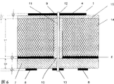
Fig. 1 has shown design form as described in the present invention, and wherein first insulating barrier (1) is made by homogenous material.On layer (5) top is the resonator plane of being made by thin copper layer (4).Between first insulating barrier (5) and second insulating barrier (7), a conductive earthing layer (6) is arranged.The thick copper layer of the nearly 1718 μ m of this ground plane (6).In plane one side microstrip circuit (8) or coupling network (3) are installed away from the described layer (7) of ground plane.Coupling point (12) and (13) link to each other by electric conductive plug (9).This plug (9) has little profile diameter, so that the input impedance of the plane resonator (4) that the position determined of Coupling point, can large-area the contact not arranged and make input impedance become uncertain with resonator surface because of plug (9).Therefore, must select the diameter of plug (9), make it enough little, so that be no more than little bandwidth of coupling network (3).So the thickness of plug (9) can not surpass 1mm.With the welding of this plug, so that can provide one to install and improved the fixedly connected of copper layer in network and the reflector plane reliably, this plug is centered on by shell (11), and this shell (11) provides hardness to reflector.
The thickness (D2) of layer (5) has determined the overall height of planar emitter basically.
Plug (9) passes in those zones of ground plane (6), and ground plane (6) has the recess (10) of a circle, and its diameter is bigger than the external diameter of plug (9).Equal the length (D2) of additives (D3) as the length of shell (11), the diameter of recess (11) must be chosen as then that the external diameter with shell (11) is the same big at least.
Layer (5) is to be made by the polystyrene of bendable foam shape, so planar emitter is to a certain degree flexible.Have only by using thin copper layer (4,6 and 8) and layer (7) just can make this flexible weakening is reduced to bottom line.
Can Coupling point (12) must not be placed on the central authorities of resonator plane by finding out among Fig. 2.By means of traditional analogy method, can calculate the required input impedance of correspondent frequency and bandwidth, can extrapolate the position of Coupling point (12) thus.
In Fig. 3, shown coupling network (3) and in or outside coupling path (16).Network (3) is made up of banded circuit (3a31) and (16).Banded conducting region has different length and width, so that has compensated the inductive part that is produced by the length of plug (9), and allows to adjust impedance, and it is focused in the ripple conducting path that leads to the plane resonator.
The conductive copper layer that in Fig. 4, has shown ground plane (6).Here stain 10,19 and 20 is represented the place that produces slit or recess on the copper.Plug (9) and (21), shell (11) and the mounting screw that is used for connector (19) provide the boring that suitable diameter is arranged by these points, so can pass this ground plane (6).
Fig. 5 has shown the profile of the expansion (24) that ripple transmission path (16) and connector (18) have been installed.Expansion (24) is positioned between connector (18) and the pressure block (22).With expansion (24) and hold-down screw connector (18) and pressure block (22) are screwed in together, so that connector (18) connects together with expansion (24) firmly, wherein the boring that is provided (23) is exactly to be used for above-mentioned screw.
The following typical geometric data that provides will be used for explanation from 2,500GHz to 2, the high system quality of the frequency spectrum inner plane type reflector of 686GHz.
Resonator plane has 47mm long, and 53mm is wide, and row and column pitch are 87mm.Feedback and Coupling point (12) are positioned at the surface and go up apart from central approximately 2mm place.It is thick that the thickness of copper layer (D1, D3 and D5) is approximately 18 μ m.Shown in figure (6), layer (5) is divided into two-layer, thereby ground floor (14) has the thickness D1 that equals 10.5mm, and by 20 kilograms/meter of its designated volume weight
3Foamed polystyrene make.The second layer (15) has the thickness D2 of 100 μ m, and is made of the heavy phthalate of polyethylene.Second insulating barrier (7) is to be made of the thick tempered glass fiber polytetrafluoroethylene of 381 μ m.
All layers all connect together each other securely, thereby layer (14) sticks on the layer (15), and binding material has 7 μ m thick.
Plug (9) has the diameter of 1.2mm, and the diameter that the one end is arranged in layer (7) is similarly the boring of 1.2mm, and passes Coupling point (13).It is the boring of 4.2mm that the circular arc that layer (5) and (6) demonstrate plug (9) is similar to the diameter that is used to insert plug (9) and shell (11).
Coupling network (3) is a symmetrical structure, can feed back all resonator plane by Coupling point (17) like this.Coupling point (13) has the internal diameter of 1.2mm and the external diameter of 2.1mm.
From arbitrary Coupling point (13) beginning, wide 0.49mm, the conductor of long 27mm (3a) is with the direction expansion of the feedback point (13) adjacent with the unit.This conductor (3a) enters wide 1.25mm afterwards, in the conductor of long 31mm (3b).Conductor (3b) enters wide 0.49mm successively afterwards, to arrive the feedback point that adjacent length is 27mm (13).Like this, the feedback point on the external resonator plane (4) in each unit links to each other with each feedback point adjacent to this unit and each resonator plane (4) under this unit.From the centre of conductor (3b), will have wide 1.86mm, the conductor of long 22.3mm (3c) links to each other with the left side direction of conductor (3b), and conductor (3c) is converted to wide 1.15mm, with the shell (conductor 3d) that is used for 42.5mm.Described afterwards conductor extends to width 1.88mm once more, and then the housing of 22.3mm has run into conductor on the other side (3b) in the middle.At conductor (3d) middle part, be arranged in rightabout conductor (3d), the wide of conductor (3c) is 1.88mm, long is 22.3mm.Next, conductor (3c) is converted to wide 1.15mm, long 129.4mm (conductor 3f).The wide 1.88mm that becomes of conductor 3f, long is 22.3mm.Like this, just reached the middle part of the conductor (3d) that is positioned at relative direction.At the middle part of conductor (3f), a wide 1.88mm is arranged, the waveguide of long 22.3mm is attached thereto, and becomes the width 1.15mm that has dwindled thus, and then links to each other with the Coupling point (21) of network (3).
By above-mentioned coupling network (3), be by the decision of the thickness of first insulating barrier (5) by the induction reactance component on the plug that self size compensated (9) of vertical plug (9).
Fig. 7 has shown that shell (11) needn't be stretched over the whole height of cover layer (5 and 6).The thickness (WS) and the length (LS) of the wall by selecting shell (11) can influence the capacity that it comprises, thereby the induction reactance component on the long plug (9) are alleviated, and are no longer needed to be used to compensate the network (3) of described reactive component.
The accompanying drawing table
1. transmitter plane
2. network plane
3. coupling network
3a-3f. tape conductor part
4. plane resonator
5. first insulating barrier
6. electronic conduction thin layer ground plane
7. second insulating barrier
8. microstripline
9. connector/coupling plug
10. through hole
11. shell
12. the feedback point of plane resonator
13. Coupling point
14. ground floor
15. the second layer
16. propagation path
17. be total to Coupling point
18. connector: N lead-in wire
19. plug recess
20. the recess of trip bolt
21. pass plug
22. pressure block
23. the boring of trip bolt
24. stretching, extension to waveguide
Claims (16)
1. planar emitter with reflector plane (1) and network plane (2), reflector plane wherein has plane resonator (4), network plane has coupling network (3), therefore a plurality of plane resonators (4) carry out phase place and electric coupling each other by described coupling network (3), it is characterized in that:
Each layer (4,5,6,7,8) of planar emitter is configured to being parallel to each other of similar sandwich, and
First insulating barrier (5) separates by an electrically conductive layer (6) and second insulating barrier (7), and this electrically conductive layer has formed common ground to reflector (1) and network (2) plane; And
First insulating barrier (5) is equipped with plane resonator (4) in its side away from electrically conductive layer (6), and
Second insulating barrier (7) is equipped with the coupling network (3) that is made of microstripline in its side away from conductive layer (6).
2. according to a kind of planar emitter of claim 1, it is characterized in that each plane resonator (4) all is to conduct electricity with coupling network (3) by conduction attachment plug (9) to be connected, thereby it is vertical with the plane of reflector (1) and network (2) to be in the interior electric Elecrical connector plug (9) of through hole.
3. according to the planar emitter of claim 2, it is characterized in that having a special circular through hole (10) in the zone that conductive plug on electrically conductive layer (9) passes, plug (9) does not exist with conductive layer (6) and is electrically connected like this.
4. according to a kind of planar emitter of claim 4, it is characterized in that described circular through hole (10) forms aperture, and by the described coupling network of diameter adjustment of aperture (10) and reflection and the transfer ratio between the corresponding plane resonator.
5. according to claim 2, a kind of planar emitter of 3 or 4, the at least a portion that it is characterized in that described each conductive plug (9) in described zone is closed by shell (11), and described zone is between the conductive layer (6) of the conductive layer (6) of described plane resonator (4) and microstripline (8).
6. according to the planar emitter of claim 5, it is characterized in that described shell (11) made the dielectric constant ε of described insulating material by insulating material especially teflon
TWith dielectric constant ε around the material of the insulating barrier (5,7) of shell (11)
TCompare, seem big especially.
7. according to a kind of planar emitter of aforementioned any claim, it is characterized in that first insulating barrier (5) is made of two kinds of insulating material, each material wherein can form a layer (14,15), thereby the thickness of ground floor (L1) is bigger than the thickness (L2) of the second layer, so the second layer (L2) is equipped with a plurality of resonator plane (14) in its side away from ground floor (14).
8. according to a kind of planar emitter of claim 7, it is characterized in that ground floor (14) is that polystyrene by foamed flexibility constitutes, especially it has 20 kilograms/meter of specific bulking values
3, thereby ground floor (14) distinguishingly has the thickness (L1) of 10.5mm.
9. according to a kind of planar emitter of claim 7 or 8, it is characterized in that the second layer (15) is the heavy phthalate thin layer of polyethylene, its thickness equals 100 μ m, and this thin layer and ground floor (14) stick together.
10. according to a kind of planar emitter of aforementioned arbitrary claim, it is characterized in that electrically conductive layer (6) has the thickness of about 18 μ m.
11. a kind of planar emitter according to aforementioned any claim, it is characterized in that wall thickness (WS), length (LS) and insulation values (constant) ε 1 by suitably selecting shell (11), can be by the induction reactance component of shell (11) compensation by thickness (D2) generation of first insulating barrier (5).
12. planar emitter according to claim 10 or 11, it is characterized in that at least in the zone that through hole (10) or plug (9) are arranged, even if having under the external force effect, the length (LS) of shell (11) still can make the distance between reflector (1) and the network plane (2) keep constant, constitutes simultaneously especially for the specified support or the strong point installed.
13. a kind of planar emitter according to aforementioned any claim, it is characterized in that by coupling network (3), compensated the induction reactance component on the described plug (9) that causes by the thickness (D2) of first insulating barrier (5) and be distributed in electric capacity on the shell (11).
14. a kind of planar emitter according to aforementioned any claim is characterized in that described plane resonator (4) is square and rectangular, particularly is arranged as two row, four row.
15., it is characterized in that the row and column spacing of described plane resonator (4) is consistent according to a kind of planar emitter of claim 14.
16. a kind of planar emitter according to aforementioned any claim, it is characterized in that the network plane (3) that is made of microstripline (8), second insulating barrier (7) and ground plane (6) extends along the form of propagation path (16), so that the waveguide side couples directly to coaxial connector (18), and need not separate planar waveguide, wherein said propagation path is between altogether between Coupling point (17) and the connector (18).
Applications Claiming Priority (2)
| Application Number | Priority Date | Filing Date | Title |
|---|---|---|---|
| DE19615497.9 | 1996-03-16 | ||
| DE19615497A DE19615497A1 (en) | 1996-03-16 | 1996-03-16 | Planar radiator |
Publications (1)
| Publication Number | Publication Date |
|---|---|
| CN1214152A true CN1214152A (en) | 1999-04-14 |
Family
ID=7791749
Family Applications (1)
| Application Number | Title | Priority Date | Filing Date |
|---|---|---|---|
| CN97193108A Pending CN1214152A (en) | 1996-03-16 | 1997-03-13 | Planar emitter |
Country Status (12)
| Country | Link |
|---|---|
| US (1) | US6204814B1 (en) |
| EP (1) | EP0886887B1 (en) |
| JP (1) | JP2000507055A (en) |
| KR (1) | KR20000064587A (en) |
| CN (1) | CN1214152A (en) |
| AT (1) | ATE185023T1 (en) |
| CA (1) | CA2250928C (en) |
| DE (2) | DE19615497A1 (en) |
| GR (1) | GR3031727T3 (en) |
| IL (1) | IL126131A (en) |
| TW (1) | TW355854B (en) |
| WO (1) | WO1997035355A1 (en) |
Families Citing this family (5)
| Publication number | Priority date | Publication date | Assignee | Title |
|---|---|---|---|---|
| GB0105251D0 (en) | 2001-03-02 | 2001-04-18 | Nokia Mobile Phones Ltd | Antenna |
| EP1239539A3 (en) * | 2001-03-02 | 2003-11-05 | Nokia Corporation | Antenna |
| US6759984B2 (en) * | 2001-06-01 | 2004-07-06 | Agere Systems Inc. | Low-loss printed circuit board antenna structure and method of manufacture thereof |
| CN112204817A (en) * | 2018-05-01 | 2021-01-08 | 韦弗有限责任公司 | Low cost dielectric for power transmission and antenna using the same |
| RU2738759C1 (en) * | 2020-06-04 | 2020-12-16 | Акционерное общество "Научно-производственная фирма "Микран" | Ultra-wideband planar emitter |
Family Cites Families (20)
| Publication number | Priority date | Publication date | Assignee | Title |
|---|---|---|---|---|
| FR2442519A1 (en) * | 1978-11-24 | 1980-06-20 | Thomson Csf | PRINTED MONOPULSE PRIMER SOURCE FOR AIRPORT RADAR ANTENNA AND ANTENNA COMPRISING SUCH A SOURCE |
| DE3514880A1 (en) * | 1984-05-22 | 1985-11-28 | Robert Bosch Gmbh, 7000 Stuttgart | Antenna array |
| EP0200819A3 (en) * | 1985-04-25 | 1987-12-09 | Robert Bosch Gmbh | Antenna array |
| US4899164A (en) * | 1988-09-16 | 1990-02-06 | The United States Of America As Represented By The Secretary Of The Air Force | Slot coupled microstrip constrained lens |
| JPH02214205A (en) * | 1989-02-14 | 1990-08-27 | Fujitsu Ltd | Electronic circuit device |
| US5001493A (en) * | 1989-05-16 | 1991-03-19 | Hughes Aircraft Company | Multiband gridded focal plane array antenna |
| FR2647599B1 (en) * | 1989-05-24 | 1991-11-29 | Alcatel Espace | CIRCUIT REALIZATION STRUCTURE AND COMPONENTS APPLIED TO MICROWAVE |
| US4973972A (en) * | 1989-09-07 | 1990-11-27 | The United States Of America As Represented By The Administrator Of The National Aeronautics And Space Adminstration | Stripline feed for a microstrip array of patch elements with teardrop shaped probes |
| US5245745A (en) * | 1990-07-11 | 1993-09-21 | Ball Corporation | Method of making a thick-film patch antenna structure |
| US5231406A (en) * | 1991-04-05 | 1993-07-27 | Ball Corporation | Broadband circular polarization satellite antenna |
| KR920022585A (en) * | 1991-05-14 | 1992-12-19 | 오오가 노리오 | Planar antenna |
| US5153600A (en) * | 1991-07-01 | 1992-10-06 | Ball Corporation | Multiple-frequency stacked microstrip antenna |
| JP2604947B2 (en) * | 1991-09-16 | 1997-04-30 | エルジー電子株式会社 | Planar antenna |
| DE4239597C2 (en) * | 1991-11-26 | 1999-11-04 | Hitachi Chemical Co Ltd | Flat antenna with dual polarization |
| JP2606521Y2 (en) * | 1992-02-27 | 2000-11-27 | 株式会社村田製作所 | Antenna device |
| US5309164A (en) * | 1992-04-13 | 1994-05-03 | Andrew Corporation | Patch-type microwave antenna having wide bandwidth and low cross-pol |
| JPH0812973B2 (en) * | 1993-04-02 | 1996-02-07 | 防衛庁技術研究本部長 | Array antenna device |
| NL9301677A (en) * | 1993-09-29 | 1995-04-18 | Hollandse Signaalapparaten Bv | Multipatch antenna. |
| DE4340825A1 (en) * | 1993-12-01 | 1995-06-08 | Rothe Lutz | Planar radiator arrangement for direct reception of the TV signals of the direct-radiating satellite system TDF 1/2 |
| US5859614A (en) * | 1996-05-15 | 1999-01-12 | The United States Of America As Represented By The Secretary Of The Army | Low-loss aperture-coupled planar antenna for microwave applications |
-
1996
- 1996-03-16 DE DE19615497A patent/DE19615497A1/en not_active Withdrawn
-
1997
- 1997-03-13 JP JP9533125A patent/JP2000507055A/en not_active Ceased
- 1997-03-13 EP EP97914238A patent/EP0886887B1/en not_active Expired - Lifetime
- 1997-03-13 DE DE59700474T patent/DE59700474D1/en not_active Expired - Fee Related
- 1997-03-13 IL IL12613197A patent/IL126131A/en not_active IP Right Cessation
- 1997-03-13 AT AT97914238T patent/ATE185023T1/en not_active IP Right Cessation
- 1997-03-13 WO PCT/EP1997/001275 patent/WO1997035355A1/en active IP Right Grant
- 1997-03-13 CN CN97193108A patent/CN1214152A/en active Pending
- 1997-03-13 KR KR1019980707236A patent/KR20000064587A/en active IP Right Grant
- 1997-03-13 US US09/142,679 patent/US6204814B1/en not_active Expired - Fee Related
- 1997-03-13 CA CA002250928A patent/CA2250928C/en not_active Expired - Fee Related
- 1997-03-15 TW TW086103233A patent/TW355854B/en active
-
1999
- 1999-11-03 GR GR990402821T patent/GR3031727T3/en unknown
Also Published As
| Publication number | Publication date |
|---|---|
| DE59700474D1 (en) | 1999-10-28 |
| KR20000064587A (en) | 2000-11-06 |
| EP0886887B1 (en) | 1999-09-22 |
| EP0886887A1 (en) | 1998-12-30 |
| IL126131A (en) | 2002-02-10 |
| GR3031727T3 (en) | 2000-02-29 |
| CA2250928A1 (en) | 1997-09-25 |
| ATE185023T1 (en) | 1999-10-15 |
| IL126131A0 (en) | 1999-05-09 |
| CA2250928C (en) | 2003-12-23 |
| JP2000507055A (en) | 2000-06-06 |
| TW355854B (en) | 1999-04-11 |
| US6204814B1 (en) | 2001-03-20 |
| WO1997035355A1 (en) | 1997-09-25 |
| DE19615497A1 (en) | 1997-09-18 |
Similar Documents
| Publication | Publication Date | Title |
|---|---|---|
| CN1209852C (en) | Source antenna for transmitting/receiving electromagnetic wave for satellite communication system | |
| AU724045B2 (en) | Antenna mutual coupling neutralizer | |
| CN1229928C (en) | Source antenna for transmitting/receiving electromagnetic wave | |
| EP0521377A2 (en) | Microstrip patch antenna structure | |
| CN1127777C (en) | Plane and double frequency aerial, radio frequency device using same | |
| EP1503451B1 (en) | Mobile radio antenna | |
| CN1223018A (en) | Antenna system | |
| CN1169387C (en) | Collapsible dipole antenna | |
| CN1897355A (en) | Internal antenna having perpendicular arrangement | |
| EP0976171B1 (en) | A method for improving antenna performance parameters and an antenna arrangement | |
| CN1720641A (en) | Multi-layer capacitive coupling in phased array antennas | |
| CN1193826A (en) | Small helical antenna with non-directional radiation pattern | |
| CN1497781A (en) | Double polarization antenna | |
| US20100194643A1 (en) | Wideband patch antenna with helix or three dimensional feed | |
| CN1875519A (en) | Antenna assembly, in particular for radar applications in motor vehicles | |
| CN111788742B (en) | Interleaved antenna array capable of operating at multiple frequencies | |
| WO2009047553A1 (en) | Phased array antenna | |
| CN1322390A (en) | Patch antenna device | |
| CN1757137A (en) | Microwave connector, antenna and method of manufacture of same | |
| EP0989628B1 (en) | Patch antenna having flexed ground plate | |
| CN1214152A (en) | Planar emitter | |
| US5339089A (en) | Antenna structure | |
| CN1250548A (en) | Microstrip distribution array for group antenna and such group antenna | |
| CN1108642C (en) | Electronics unit for radio transmission of signal | |
| US6040802A (en) | Antenna cross-polar suppression means |
Legal Events
| Date | Code | Title | Description |
|---|---|---|---|
| C06 | Publication | ||
| PB01 | Publication | ||
| C10 | Entry into substantive examination | ||
| SE01 | Entry into force of request for substantive examination | ||
| C02 | Deemed withdrawal of patent application after publication (patent law 2001) | ||
| WD01 | Invention patent application deemed withdrawn after publication | ||
| REG | Reference to a national code |
Ref country code: HK Ref legal event code: WD Ref document number: 1018852 Country of ref document: HK |