CN1209822C - Channel metallic-oxide-semiconductor device and terminal structure - Google Patents
Channel metallic-oxide-semiconductor device and terminal structure Download PDFInfo
- Publication number
- CN1209822C CN1209822C CNB011416785A CN01141678A CN1209822C CN 1209822 C CN1209822 C CN 1209822C CN B011416785 A CNB011416785 A CN B011416785A CN 01141678 A CN01141678 A CN 01141678A CN 1209822 C CN1209822 C CN 1209822C
- Authority
- CN
- China
- Prior art keywords
- groove
- terminal structure
- layer
- semiconductor substrate
- mos device
- Prior art date
- Legal status (The legal status is an assumption and is not a legal conclusion. Google has not performed a legal analysis and makes no representation as to the accuracy of the status listed.)
- Expired - Lifetime
Links
- 239000004065 semiconductor Substances 0.000 title claims abstract description 54
- 239000000758 substrate Substances 0.000 claims abstract description 73
- 239000012535 impurity Substances 0.000 claims description 22
- 229910021417 amorphous silicon Inorganic materials 0.000 claims description 10
- 239000002184 metal Substances 0.000 claims description 10
- 229910052751 metal Inorganic materials 0.000 claims description 10
- 229910021420 polycrystalline silicon Inorganic materials 0.000 claims description 10
- 229920005591 polysilicon Polymers 0.000 claims description 10
- 238000002955 isolation Methods 0.000 claims description 5
- 239000000463 material Substances 0.000 claims description 4
- 238000000034 method Methods 0.000 description 23
- 238000005516 engineering process Methods 0.000 description 20
- 230000008569 process Effects 0.000 description 11
- 230000003647 oxidation Effects 0.000 description 9
- 238000007254 oxidation reaction Methods 0.000 description 9
- 230000005684 electric field Effects 0.000 description 7
- BOTDANWDWHJENH-UHFFFAOYSA-N Tetraethyl orthosilicate Chemical group CCO[Si](OCC)(OCC)OCC BOTDANWDWHJENH-UHFFFAOYSA-N 0.000 description 6
- 238000004519 manufacturing process Methods 0.000 description 6
- 229920002120 photoresistant polymer Polymers 0.000 description 6
- 230000015572 biosynthetic process Effects 0.000 description 4
- 239000004020 conductor Substances 0.000 description 4
- 239000000428 dust Substances 0.000 description 4
- 230000015556 catabolic process Effects 0.000 description 3
- 238000005530 etching Methods 0.000 description 3
- 238000002360 preparation method Methods 0.000 description 3
- 238000004544 sputter deposition Methods 0.000 description 3
- XUIMIQQOPSSXEZ-UHFFFAOYSA-N Silicon Chemical compound [Si] XUIMIQQOPSSXEZ-UHFFFAOYSA-N 0.000 description 2
- 210000003323 beak Anatomy 0.000 description 2
- 238000006243 chemical reaction Methods 0.000 description 2
- 239000011248 coating agent Substances 0.000 description 2
- 238000000576 coating method Methods 0.000 description 2
- 238000000151 deposition Methods 0.000 description 2
- 238000000407 epitaxy Methods 0.000 description 2
- 238000005468 ion implantation Methods 0.000 description 2
- 238000004518 low pressure chemical vapour deposition Methods 0.000 description 2
- 238000001259 photo etching Methods 0.000 description 2
- 238000004220 aggregation Methods 0.000 description 1
- 230000002776 aggregation Effects 0.000 description 1
- 230000004888 barrier function Effects 0.000 description 1
- 238000004891 communication Methods 0.000 description 1
- 238000007796 conventional method Methods 0.000 description 1
- 238000002425 crystallisation Methods 0.000 description 1
- 230000008025 crystallization Effects 0.000 description 1
- 230000008021 deposition Effects 0.000 description 1
- 238000009792 diffusion process Methods 0.000 description 1
- 238000001312 dry etching Methods 0.000 description 1
- 230000005669 field effect Effects 0.000 description 1
- 238000011049 filling Methods 0.000 description 1
- 239000003292 glue Substances 0.000 description 1
- 230000006872 improvement Effects 0.000 description 1
- 229910044991 metal oxide Inorganic materials 0.000 description 1
- 150000004706 metal oxides Chemical class 0.000 description 1
- 238000001465 metallisation Methods 0.000 description 1
- 125000004430 oxygen atom Chemical group O* 0.000 description 1
- 238000000206 photolithography Methods 0.000 description 1
- 238000000623 plasma-assisted chemical vapour deposition Methods 0.000 description 1
- 230000002028 premature Effects 0.000 description 1
- 229910052710 silicon Inorganic materials 0.000 description 1
- 239000010703 silicon Substances 0.000 description 1
Images


Classifications
-
- H—ELECTRICITY
- H01—ELECTRIC ELEMENTS
- H01L—SEMICONDUCTOR DEVICES NOT COVERED BY CLASS H10
- H01L29/00—Semiconductor devices adapted for rectifying, amplifying, oscillating or switching, or capacitors or resistors with at least one potential-jump barrier or surface barrier, e.g. PN junction depletion layer or carrier concentration layer; Details of semiconductor bodies or of electrodes thereof ; Multistep manufacturing processes therefor
- H01L29/66—Types of semiconductor device ; Multistep manufacturing processes therefor
- H01L29/68—Types of semiconductor device ; Multistep manufacturing processes therefor controllable by only the electric current supplied, or only the electric potential applied, to an electrode which does not carry the current to be rectified, amplified or switched
- H01L29/76—Unipolar devices, e.g. field effect transistors
- H01L29/772—Field effect transistors
- H01L29/78—Field effect transistors with field effect produced by an insulated gate
- H01L29/7801—DMOS transistors, i.e. MISFETs with a channel accommodating body or base region adjoining a drain drift region
- H01L29/7802—Vertical DMOS transistors, i.e. VDMOS transistors
- H01L29/7813—Vertical DMOS transistors, i.e. VDMOS transistors with trench gate electrode, e.g. UMOS transistors
-
- H—ELECTRICITY
- H01—ELECTRIC ELEMENTS
- H01L—SEMICONDUCTOR DEVICES NOT COVERED BY CLASS H10
- H01L29/00—Semiconductor devices adapted for rectifying, amplifying, oscillating or switching, or capacitors or resistors with at least one potential-jump barrier or surface barrier, e.g. PN junction depletion layer or carrier concentration layer; Details of semiconductor bodies or of electrodes thereof ; Multistep manufacturing processes therefor
- H01L29/02—Semiconductor bodies ; Multistep manufacturing processes therefor
- H01L29/06—Semiconductor bodies ; Multistep manufacturing processes therefor characterised by their shape; characterised by the shapes, relative sizes, or dispositions of the semiconductor regions ; characterised by the concentration or distribution of impurities within semiconductor regions
- H01L29/0657—Semiconductor bodies ; Multistep manufacturing processes therefor characterised by their shape; characterised by the shapes, relative sizes, or dispositions of the semiconductor regions ; characterised by the concentration or distribution of impurities within semiconductor regions characterised by the shape of the body
- H01L29/0661—Semiconductor bodies ; Multistep manufacturing processes therefor characterised by their shape; characterised by the shapes, relative sizes, or dispositions of the semiconductor regions ; characterised by the concentration or distribution of impurities within semiconductor regions characterised by the shape of the body specially adapted for altering the breakdown voltage by removing semiconductor material at, or in the neighbourhood of, a reverse biased junction, e.g. by bevelling, moat etching, depletion etching
-
- H—ELECTRICITY
- H01—ELECTRIC ELEMENTS
- H01L—SEMICONDUCTOR DEVICES NOT COVERED BY CLASS H10
- H01L29/00—Semiconductor devices adapted for rectifying, amplifying, oscillating or switching, or capacitors or resistors with at least one potential-jump barrier or surface barrier, e.g. PN junction depletion layer or carrier concentration layer; Details of semiconductor bodies or of electrodes thereof ; Multistep manufacturing processes therefor
- H01L29/40—Electrodes ; Multistep manufacturing processes therefor
- H01L29/402—Field plates
- H01L29/407—Recessed field plates, e.g. trench field plates, buried field plates
-
- H—ELECTRICITY
- H01—ELECTRIC ELEMENTS
- H01L—SEMICONDUCTOR DEVICES NOT COVERED BY CLASS H10
- H01L29/00—Semiconductor devices adapted for rectifying, amplifying, oscillating or switching, or capacitors or resistors with at least one potential-jump barrier or surface barrier, e.g. PN junction depletion layer or carrier concentration layer; Details of semiconductor bodies or of electrodes thereof ; Multistep manufacturing processes therefor
- H01L29/66—Types of semiconductor device ; Multistep manufacturing processes therefor
- H01L29/66007—Multistep manufacturing processes
- H01L29/66075—Multistep manufacturing processes of devices having semiconductor bodies comprising group 14 or group 13/15 materials
- H01L29/66083—Multistep manufacturing processes of devices having semiconductor bodies comprising group 14 or group 13/15 materials the devices being controllable only by variation of the electric current supplied or the electric potential applied, to one or more of the electrodes carrying the current to be rectified, amplified, oscillated or switched, e.g. two-terminal devices
- H01L29/6609—Diodes
- H01L29/66143—Schottky diodes
-
- H—ELECTRICITY
- H01—ELECTRIC ELEMENTS
- H01L—SEMICONDUCTOR DEVICES NOT COVERED BY CLASS H10
- H01L29/00—Semiconductor devices adapted for rectifying, amplifying, oscillating or switching, or capacitors or resistors with at least one potential-jump barrier or surface barrier, e.g. PN junction depletion layer or carrier concentration layer; Details of semiconductor bodies or of electrodes thereof ; Multistep manufacturing processes therefor
- H01L29/66—Types of semiconductor device ; Multistep manufacturing processes therefor
- H01L29/66007—Multistep manufacturing processes
- H01L29/66075—Multistep manufacturing processes of devices having semiconductor bodies comprising group 14 or group 13/15 materials
- H01L29/66227—Multistep manufacturing processes of devices having semiconductor bodies comprising group 14 or group 13/15 materials the devices being controllable only by the electric current supplied or the electric potential applied, to an electrode which does not carry the current to be rectified, amplified or switched, e.g. three-terminal devices
- H01L29/66234—Bipolar junction transistors [BJT]
- H01L29/66325—Bipolar junction transistors [BJT] controlled by field-effect, e.g. insulated gate bipolar transistors [IGBT]
- H01L29/66333—Vertical insulated gate bipolar transistors
- H01L29/66348—Vertical insulated gate bipolar transistors with a recessed gate
-
- H—ELECTRICITY
- H01—ELECTRIC ELEMENTS
- H01L—SEMICONDUCTOR DEVICES NOT COVERED BY CLASS H10
- H01L29/00—Semiconductor devices adapted for rectifying, amplifying, oscillating or switching, or capacitors or resistors with at least one potential-jump barrier or surface barrier, e.g. PN junction depletion layer or carrier concentration layer; Details of semiconductor bodies or of electrodes thereof ; Multistep manufacturing processes therefor
- H01L29/66—Types of semiconductor device ; Multistep manufacturing processes therefor
- H01L29/68—Types of semiconductor device ; Multistep manufacturing processes therefor controllable by only the electric current supplied, or only the electric potential applied, to an electrode which does not carry the current to be rectified, amplified or switched
- H01L29/70—Bipolar devices
- H01L29/72—Transistor-type devices, i.e. able to continuously respond to applied control signals
- H01L29/739—Transistor-type devices, i.e. able to continuously respond to applied control signals controlled by field-effect, e.g. bipolar static induction transistors [BSIT]
- H01L29/7393—Insulated gate bipolar mode transistors, i.e. IGBT; IGT; COMFET
- H01L29/7395—Vertical transistors, e.g. vertical IGBT
- H01L29/7396—Vertical transistors, e.g. vertical IGBT with a non planar surface, e.g. with a non planar gate or with a trench or recess or pillar in the surface of the emitter, base or collector region for improving current density or short circuiting the emitter and base regions
- H01L29/7397—Vertical transistors, e.g. vertical IGBT with a non planar surface, e.g. with a non planar gate or with a trench or recess or pillar in the surface of the emitter, base or collector region for improving current density or short circuiting the emitter and base regions and a gate structure lying on a slanted or vertical surface or formed in a groove, e.g. trench gate IGBT
-
- H—ELECTRICITY
- H01—ELECTRIC ELEMENTS
- H01L—SEMICONDUCTOR DEVICES NOT COVERED BY CLASS H10
- H01L29/00—Semiconductor devices adapted for rectifying, amplifying, oscillating or switching, or capacitors or resistors with at least one potential-jump barrier or surface barrier, e.g. PN junction depletion layer or carrier concentration layer; Details of semiconductor bodies or of electrodes thereof ; Multistep manufacturing processes therefor
- H01L29/66—Types of semiconductor device ; Multistep manufacturing processes therefor
- H01L29/68—Types of semiconductor device ; Multistep manufacturing processes therefor controllable by only the electric current supplied, or only the electric potential applied, to an electrode which does not carry the current to be rectified, amplified or switched
- H01L29/76—Unipolar devices, e.g. field effect transistors
- H01L29/772—Field effect transistors
- H01L29/78—Field effect transistors with field effect produced by an insulated gate
- H01L29/7801—DMOS transistors, i.e. MISFETs with a channel accommodating body or base region adjoining a drain drift region
- H01L29/7802—Vertical DMOS transistors, i.e. VDMOS transistors
- H01L29/7811—Vertical DMOS transistors, i.e. VDMOS transistors with an edge termination structure
-
- H—ELECTRICITY
- H01—ELECTRIC ELEMENTS
- H01L—SEMICONDUCTOR DEVICES NOT COVERED BY CLASS H10
- H01L29/00—Semiconductor devices adapted for rectifying, amplifying, oscillating or switching, or capacitors or resistors with at least one potential-jump barrier or surface barrier, e.g. PN junction depletion layer or carrier concentration layer; Details of semiconductor bodies or of electrodes thereof ; Multistep manufacturing processes therefor
- H01L29/66—Types of semiconductor device ; Multistep manufacturing processes therefor
- H01L29/86—Types of semiconductor device ; Multistep manufacturing processes therefor controllable only by variation of the electric current supplied, or only the electric potential applied, to one or more of the electrodes carrying the current to be rectified, amplified, oscillated or switched
- H01L29/861—Diodes
- H01L29/872—Schottky diodes
- H01L29/8725—Schottky diodes of the trench MOS barrier type [TMBS]
Abstract
A termination structure for power trench MOS devices is disclosed. The MOS devices can be Schottky diode, IGBT or DMOS depending on what kinds of the semiconductor substrate are prepared. The termination structure comprises: a semiconductor substrate having a trench formed therein; a spacer-like MOS gate formed on a sidewall of the trench; a termination structure oxide layer formed in the trench to cover a portion of the spacer-like MOS gate and to cover a bottom of the trench; and a first electrode and a second electrode are, respectively, formed on a bottom surface and upper surface of the semiconductor substrate. The trench is formed from a boundary of the active region to an edge of the semiconductor substrate. The trench MOS devices are formed in the active region. In addition for IGBT and DMOS, the second electrode is isolated from MOS gate by an oxide layer; however, for Schottky diode, the second electrode is directed contact to the MOS gate.
Description
Technical field
The present invention relates to semiconductor device, particularly relate to the novel terminal structure of the groove MOS device that prevents leakage current.
Background technology
MOS mos field effect transistor (DMOSFET), insulated gate bipolar transistor (IGBT) and Schottky diode all are important power devices, and they are widely used as the output rectifying tube in switched-mode power supply and other high-speed power switch application.For example, application comprises: motor-drive circuit, communication exchange equipment, industrial automation and automatic electronic.Usually, require power device to bear big forward current, high reverse bias cut-ff voltage, for example be higher than 30 volts, and reverse bias leakage current is reduced to minimum.Existing several reports propose groove MOS, trench IGBT and trench schottky diode and are better than the device that those have planar structure.
About power transistor, except requiring this device active area passes through big electric current, the active area terminal on every side that also requires to be usually located at the tube core end has a kind of like this structural design, promptly prevents to occur too early the voltage breakdown phenomenon.The tradition terminal structure comprises local oxidation of silicon layer (LOCOS), field plate, guard ring or their combination.Known LOCOS has beak shape feature usually.Occur the electric field aggregation phenomenon in beak easily, this is because the impact ionization rate height.Therefore, can increase leakage current and worsen the electrical characteristics of active area.
For example, please refer to Fig. 1, Fig. 1 shows Semiconductor substrate with the trench MOS structure that is used for Schottky diode and the groove terminal structure that forms within it.This substrate is heavy doping n
+Substrate 10 and be formed with epitaxial loayer 20 thereon.In epitaxial loayer 20, form a plurality of groove MOSs 15.Form the groove MOS device that comprises epitaxial loayer 20/ grid oxic horizon 25/ polysilicon layer 30 at active area 5.The border of active area 5 is the LOCOS district that the thickness that utilizes conventional method to form is about 6000 dusts to the edge of tube core.
Gather problem in order to alleviate electric field, utilize ion implantation technique below the LOCOS district, to form P
+Doped region 50.P
+Doped region 50 is the guard rings that are used to strengthen the reverse bias cut-ff voltage.Anode (metal level) 55 is formed on the active area 5 and at the P in whole LOCOS district
+Extend on the doped region 50.Purpose is to make the buckled zone of depletion boundaries away from active area 5.Although guard ring 50 can be alleviated electric field and gather and reduce near the flexibility that appears at the active area, as shown in arrow 60, P
+Adjacent region between the below of district 50 and groove MOS device bottom is not a smooth curved.It can increase leakage current and reduce the reverse bias block capability.Analogue also occurs under field plate and the situation that guard ring combines.In addition, above-mentioned conventional art requires to make more photomask (at least 4), so technology is quite complicated.Another disadvantage is the cost height that forms this structure.
Because above-mentioned several traditional terminal structures all can not thoroughly be dealt with problems, so an object of the present invention is to propose a kind of novel terminal structure.This novel terminal structure can make the buckled zone of depletion region away from active area, and depletion boundaries is also straight than the depletion boundaries of above-mentioned prior art.Manufacture method provided by the invention is simpler than the manufacture method of prior art.Owing to form terminal structure and groove simultaneously, so only need 3 photomasks, technology is simple, cost is low.
Summary of the invention
The invention discloses a kind of novel terminal structure that can form simultaneously with groove MOS device.Which kind of Semiconductor substrate according to what prepare is, but MOS device Schottky diode, DMOS or IGBT.Terminal structure and groove MOS device comprise: Semiconductor substrate has second groove that is formed at active area and spaced a plurality of first grooves and forms to the end of Semiconductor substrate from the border of active area; Be formed at the first type mos gate and second mos gate that is formed on the sidewall of second groove in each first groove as sept; Be formed on the terminal structure oxide layer in second groove, in order to a part that covers sept and the bottom that covers second groove; First electrode and second electrode are respectively formed on the lower surface and upper surface of Semiconductor substrate.The residing position of second electrode can make it cover from active area through the zone of sept to the part of terminal structure oxide layer, so that the buckled zone of depletion region is away from active area.
Description of drawings
With reference to following detailed description, above-mentioned each side of the present invention and the many advantages that had will become easier to understand in conjunction with the drawings, wherein:
Fig. 1 shows the conventional groove schottky diode device and as the LOCOS supplementary protection ring of terminal structure;
Fig. 2 shows first groove that forms according to the present invention and the cutaway view of second groove on Semiconductor substrate;
Fig. 3 shows the cutaway view that utilizes the first electric conducting material backfill, first groove and second groove according to the present invention;
Fig. 4 shows the cutaway view of the terminal structure oxide layer that limits in order to expose active area and sept according to the present invention;
Fig. 5 A shows according to the present invention the anode electrode that forms in the both sides of Semiconductor substrate in order to realize Schottky diode and terminal structure and the cutaway view of cathode electrode;
Fig. 5 B shows utilization according to Schottky diode of the present invention and the equipotential lines of terminal structure acquisition and the analog result of power line;
Fig. 5 C shows the analog result that has and do not have the leakage current of the trench schottky diode of terminal structure according to the present invention;
Fig. 6 shows according to the present invention the cutaway view of the Semiconductor substrate that is the preparation of DMOS device and terminal structure;
Fig. 7 shows dark etched first conductor layer according to the present invention, carries out the high temperature thermal oxidation metallization processes then to form the cutaway view of conduction interlevel oxide layer;
Fig. 8 shows the cutaway view of the terminal structure oxide layer that limits in order to expose active area and sept according to the present invention;
Fig. 9 shows according to the present invention the source electrode that forms in the both sides of Semiconductor substrate in order to realize DMOS device and terminal structure and the cutaway view of drain electrode;
Figure 10 shows according to the present invention the cutaway view of the Semiconductor substrate that is the preparation of IGBT and terminal structure;
Figure 11 shows the cutaway view of the terminal structure oxide layer that limits in order to expose active area and sept according to the present invention;
Figure 12 shows the cutaway view of the emitter and collector that forms in the both sides of Semiconductor substrate in order to realize IGBT and terminal structure according to the present invention;
Embodiment
As described in the above-mentioned background technology, traditional terminal structure comprises localized oxide, field plate, guard ring or their combination, and all these all can not thoroughly solve electric field and gather problem.According to design difference, electric field still can occur at diverse location and gather.The present invention proposes a kind of novel groove terminal structure and manufacture method thereof.This novel groove terminal structure can overcome electric field and gather problem.Novel groove terminal provides straight depletion boundaries, and its buckled zone has also weakened reverse bias voltage simultaneously away from active area.Therefore, this novel terminal structure can prevent to occur too early punch-through.
In addition, novel terminal structure can be applied to any power transistor, for example Schottky Rectifier, DMOS, IGBT etc.The most important thing is to form groove MOS device and groove terminal structure simultaneously.
Below several exemplary embodiments will be described successively.
First preferred embodiment is used to illustrate the method that forms groove terminal structure and Schottky diode simultaneously.
Please refer to Fig. 2, cutaway view shown in Figure 2 shows Semiconductor substrate 100, and Semiconductor substrate 100 comprises that the ground floor 100A that is doped with first conductive type impurity (for example n type) and heavy doping have first conductive type impurity (n for example
+) base substrate 100B.Extension forms ground floor 100A to form Schottky contacts on base substrate 100B, and base substrate is used to form ohmic contact, forms metal level simultaneously thereon.
Then, utilize CVD on the first substrate 100A, to form the oxide layer 101 of thick about 2000 dusts-10000 dust.Then, on oxide layer 101, apply the photoresist (not shown) to limit a plurality of first grooves 110 and second groove 120.According to cutaway view, it is wide that each first groove 110 is about 0.2-2.0 μ m at active area.Tableland 115 separates second groove 120 and first groove 110, and arrives formation second groove 120 between the end of Semiconductor substrate 100 (or tube core) on the active area border.Second groove 120 is used to produce straight depletion boundaries and prevents that electric field from gathering.
With reference to figure 3, after the removal oxide layer 101, carry out high temperature oxidation process to form grid oxic horizon 125.On sidewall 110A, the sidewall 120A of first groove 110 and second groove 120, bottom 110B, bottom 120B, form the grid oxic horizon 125 of thickness between 150 dust to 3000 dusts.Perhaps, can also utilize high-temperature deposition technology to form grid oxic horizon 125 to form HTO (high-temperature oxide deposit) layer.
Then, utilize CVD, it highly is higher than tableland 115 at least to form first conductive layer 140 and backfill first groove 110 and second groove 120 on grid oxic horizon 125.Because CVD technology also is formed with first conductive layer 140 at the back side of Semiconductor substrate 100E.First conductive is the material of selecting from the group that comprises metal, polysilicon and amorphous silicon.First conductive layer 140 preferably is about 0.5 μ m to 3.0 μ m.For the space appears in the inside that prevents first groove, the preferred material that adopts the polysilicon layer of LPCVD (low pressure chemical vapor deposition) formation as ground floor 140 with step coverage rate.Yet, if the ratio of width to height of first groove 110 greater than 5, preferentially adopts the amorphous silicon that utilizes PECVD to form.Amorphous silicon has gap-filling property preferably than polysilicon.Certainly, have conductive characteristic, need carry out crystallization processes again amorphous silicon in order to make amorphous silicon.
Please refer to Fig. 4,, utilize grid oxic horizon 125 on the tableland 115, carry out anisotropic etching as etch stop layer in order to remove the first unnecessary conductive layer 140 on the 115A of tableland.After this technology, on the sidewall 120A of second groove 120, form the sept 122 that its width (along cutaway view) is about the degree of depth of second groove.
After this, form the dielectric layer 150 of terminal structure.Dielectric layer is TEOS layer or HTO layer, and the TEOS layer is LPTEOS, PETEOS or O
3-TEOS.Dielectric layer 150 is between 0.2-1.0 μ m.
Then, in order to limit the scope of Schottky contacts, coating photoresist figure 155 on dielectric layer 150.Then, utilize photoresist figure 155 to carry out tableland 115A and first conductive layer 140 of dry etching to expose first groove 110 as mask.
With reference to figure 5, behind the stripping photolithography glue pattern 155, the unnecessary layer of removing the back side is to expose the surface of base substrate 100B.Unnecessary layer is because will make device in active area carries out thermal oxidation technology or CVD technology, and those layers that form at the back side of Semiconductor substrate, they comprise dielectric layer 150, first conductive layer 140 and grid oxic horizon 125.
After this, carry out sputtering technology, thereby between second conductive layer and the second substrate 100B, form the negative electrode 160 that belongs to ohmic contact in formation Schottky contact region 115 between second conductive layer and the first substrate 100A with deposit second conductive layer.At last, on second conductive layer, form photoresist figure 165 to limit anode electrode 160A.In a preferred embodiment, form anode 160A from the active area that extends to second groove 120 to the zone of leaving active area 2.0 μ m at least.Therefore, the buckled zone of depletion region can be away from active area.
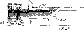
Fig. 5 B shows one of electrical characteristics of groove MOS terminal structure (shown in Fig. 5 A).For example, for the simulated inverse biasing, Schottky diode is applied reverse bias.Therefore, for example, negative electrode 160 is applied with 100 volts voltage, and anode is applied with 0 volt voltage.Numbering 180 expression equipotential liness.In Fig. 5 B, the voltage that bears on the equipotential lines reduces gradually from down to up.The line vertical with equipotential lines 180 represented power line.As shown in the figure, only produce leakage current, and in the depletion region under the terminal region, almost do not have leakage current at active area.In addition, the depletion region border of being represented by symbol 180A has falt characteristic, therefore can not occur voltage breakdown too early.A little leakage current is only arranged.
Fig. 5 C shows does not have terminal structure 195 and the comparable situation that has according to the groove MOS reverse current curve of terminal structure 190 of the present invention.Terminal structure can only increase by 8.8% with reverse current.On the contrary, in traditional terminal structure that LOCOS combines with guard ring, can produce 12.8%.Therefore the invention provides tangible improvement.In addition, conventional fabrication processes needs 4 photomasks at least, and the present invention only needs 3 photomasks (for example, form groove (first photomask), contact definite (second photomask), and etching forming second conductive layer (the 3rd photomask) of anode).The present invention provides simpler technology.
Employing can form groove DMOS structure and terminal structure according to second preferred embodiment of terminal structure of the present invention.
With reference to figure 6, for the DMOS structure, the Semiconductor substrate of preparation is different with the situation that forms Schottky diode, but it is closely similar to form technology.In order to form DMOS and terminal structure simultaneously, at first Semiconductor substrate 200 comprises from top to bottom and utilizes ground floor 200A, second layer 200B and base substrate 200C.Ground floor 200A and second layer 200B are formed on the base substrate 200C by epitaxy technique
The ground floor 200A that is doped with p type conductive impurity is the doped layer 203 that heavy doping has p type conductive impurity on ground floor 200A as bottom then.Second layer 200B is doped with n type conductive impurity, and the 3rd layer of 200C heavy doping has n type impurity.In addition, as shown in Figure 6, utilize ion implantation technique, form a plurality of n on the top of ground floor 200A
+The district is to cut off p
+Thereby layer 203 forms many n
+ District 204 and p
+District 203.The thickness of ground floor 200A and second layer 200B is respectively 0.5 μ m-5.0 μ m and 3 μ m to 30 μ m.
After this, please refer to Fig. 7,, at first form a plurality of first groove 210 and second grooves 220 that between them, have tableland 215 as according to the described method of first preferred embodiment.Pass through n
+ District 204 forms first groove 210 at active area, and the end from the border of active area to Semiconductor substrate 200 (or tube core) forms second groove 220.
Then, carry out high temperature oxidation process to form the grid oxic horizon 225 of thickness between 150 dust to 3000 dusts.Then, the conductive layer 240 that will select in first polysilicon or the amorphous silicon is backfilling into first groove 210 and second groove 220 and exceeds tableland 215.Utilize grid oxic horizon 225 on the 215A of tableland as etch stop layer, carry out dark etched step to remove unnecessary conductive layer 240.Use n then
+ District 204 and p
+District 203 is as the gate oxide 225 of barrier layer removal on the tableland.
Then, carry out another time thermal oxidation technology to form conduction interlevel oxide layer 245 by oxidized portion first conductive layer 240.Because the grain boundary of polysilicon can provide the path of oxygen atom rapid diffusion, thus in first groove 210 and second groove 220, utilize oxide layer that polysilicon or amorphous silicon form than the oxidation bed thickness that on Semiconductor substrate and tableland 215A, forms many.
With reference to figure 8, carry out dark etched step with remove on the ground floor 200A surface, n
+District 204 and P
+ Thermal oxide layer 245 in the district 203.It should be noted that after the step of isolation features is provided, on the sept 240 of second groove 220 and on the upper surface of first conductive layer 240, still have thermal oxide layer 245.Then, in all each districts, form TEOS oxide layer 250.On the TEOS of ground floor 200A oxide layer 250, form the photoresist figure to limit source contact area.
With reference to figure 9, before carrying out sputtering technology, at first remove the unnecessary layer that the back side (or claiming base substrate 200C) in Semiconductor substrate forms.Unnecessary layer comprises TEOS oxide layer 250, conduction interlevel oxide layer 245, first conductive layer 240 and the lip-deep grid oxic horizon 225 of substrate 200C, and they form when being devices in making active area simultaneously.
Then, carry out the depositing technics of metal level 260 to form the source electrode contact on the ground floor 200A and on substrate 200C, promptly to form the drain electrode contact by sputter at the back side of Semiconductor substrate.With identical in the past, thereby the metal level 260 that still requires to form on active area expands to spaced apart with active area apart from terminal structure 220 at least 2.0 μ m.For this reason, with former identical photoetching process and the etch process of carrying out continuously.
Employing is to form trench IGBT structure and terminal structure synchronously according to the 3rd preferred embodiment of terminal structure of the present invention.
With reference to Figure 10, for will be as the groove MOS of IGBT structure, prepared Semiconductor substrate be different with the situation that forms Schottky diode, but very similar with the Semiconductor substrate that is used for trench-dmos devices.In addition, the manufacturing process of technology and manufacturing groove DMOS much at one.In order to form IGBT and terminal structure simultaneously, at first prepared Semiconductor substrate 300 comprises ground floor 300A, second layer 300B, the 3rd layer of 300C and base substrate 300D from top to bottom.Utilize epitaxy technique, on base substrate 300D, form ground floor 300A, second layer 300B and the 3rd layer of 300C.
The doping content of the ground floor 300A of doping type, second layer 300B and the 3rd layer of 300C is identical with the doping content of Semiconductor substrate shown in Figure 6.For example, ground floor 300A is a p type bottom, has top n on the top of p substrate layer 302
+ District 304 and p
+District 303.Second layer 300B is the n-doped layer as the drift region, and the 3rd layer of 300C is n
+Layer.Yet substrate 300D is a p type conductive impurity heavily doped region.The thickness of ground floor 300A and second layer 300B is respectively 0.5 μ m-10.0 μ m and 3 μ m-100 μ m.
With reference to Figure 11, pass through n
+ Doped region 304 forms a plurality of first grooves 310.The bottom of first groove 310 is lower than p type doped layer 302.In addition, between second groove 320 and each first groove respectively with tableland 315 isolation of 0.2 μ m to 4.0 μ m.Second groove 320 is formed on the border of active area and extends to the edge of Semiconductor substrate.
After the thermal oxidation technology of having finished the grid oxic horizon of formation thickness between 150 dust to 3000 dusts, deposit utilizes the fill process such as first electric conducting material 340 of polysilicon layer or amorphous silicon layer on first groove 310 and second groove 320.Then, utilize tableland 315 lip-deep grid oxic horizons 325 to carry out dark etch process, so that have only the sept in first groove and second groove to have first electric conducting material 340 as etch stop layer.
Identical with above-mentioned second embodiment, remove the lip-deep grid oxic horizon 325 of ground floor, then, carry out another thermal oxidation technology technology and isolate with the conduction interlevel oxide layer 345 and the metal level (back forms) that form conductive layer 340.After this, the portion of hot oxide layer on first conductive layer in keeping first groove 310 and second groove 320 is removed the thermal oxide layer 345 of tableland 315A top as the conduction interlevel oxide layer.
Continuation with identical in the past, is carried out the technology of deposit TEOS dielectric layer 350 on all each districts and the technology of coating photoresist figure with reference to Figure 11 continuously.After this, carry out etching technics to expose n
+ Doped region 204 and P
+Doped region.
Figure 12 shows the unnecessary layer at the back side of removing before the splash-proofing sputtering metal on base substrate.Usually, after having formed second conductive layer, on the surface of substrate 300D, form metal level to form collector electrode.After carrying out photoetching process and etch process continuously, at contact p
+District 303 and n
+Form emitter on the surface of the 300A in district 304, it contacts with n+ district 304 with p+ district 303.One end of emitter is away from active area.
The invention has the advantages that:
(1) buckled zone of the straight and depletion boundaries of depletion boundaries is away from active area.These two characteristics can prevent premature breakdown voltage phenomenon.
(2) leakage current that produces during reverse bias of terminal structure of the present invention adds the leakage current (8.8% to 12.8%) that the guard ring terminal structure produces less than traditional LOCOS.
(3) it is simple to make the method that the method for the groove MOS device with terminal structure makes groove MOS device than conventional art.The photomask that terminal structure of the present invention needs still less.
In the present technique field those of skill in the art understood, just the present invention will be described for the preferred embodiment of the invention described above to its meaning without limits.Claimed various conversion scheme and the similar scheme that is included in the described essential scope of claims, explanation comprises all these conversion scheme and similar structures thereby its scope should provide the most widely.
Claims (22)
1. the terminal structure of a groove MOS device, described terminal structure comprises:
Semiconductor substrate wherein is formed with groove, and to the end of described Semiconductor substrate, described groove MOS is formed at the described active region of described Semiconductor substrate to described groove from the border of active area;
Mos gate is formed on as sept on the sidewall of described groove;
The terminal structure oxide layer is formed in the described groove, covers the part of described sept and covers the bottom of described groove; With
First conductive layer as first electrode, is formed on the bottom surface of described Semiconductor substrate; Second conductive layer as second electrode, is formed on the upper surface of described Semiconductor substrate, and the described upper surface of wherein said Semiconductor substrate is through the zone of described sept to the part of described terminal structure oxide layer from described active area.
2. according to the described terminal structure of claim 1, the degree of depth of wherein said groove is between 0.4-10 μ m.
3. according to the described terminal structure of claim 1, wherein said mos gate comprises the conductive layer that is formed on the gate oxide.
4. according to the described terminal structure of claim 1, wherein said groove MOS device comprises power transistor.
5. according to the described terminal structure of claim 4, wherein according to provide which kind of described Semiconductor substrate and described have the conduction interlevel oxide layer grid whether the conductive layer and described second electrode isolation of described mos gate are opened, described power transistor is selected from the group that Schottky diode, DMOS and IGBT constituted.
6. the terminal structure of a groove MOS device, described terminal structure and described groove MOS device comprise:
Semiconductor substrate wherein is formed with first groove and second groove, and first groove is formed on active area, and second groove is formed on from the border of described active area to the zone of the end of described Semiconductor substrate;
Be formed at first mos gate in described first groove and be formed at second mos gate on the sidewall of described second groove as sept;
The terminal structure oxide layer is formed in described second groove, covers the part of described sept and covers the bottom of described second groove; With
Conductive layer, the conductive layer of lower surface that wherein is formed on described Semiconductor substrate be as first electrode, is formed on conductive layer on the upper surface of described Semiconductor substrate as second electrode.
7. according to the terminal structure of the described groove MOS device of claim 6, wherein said Semiconductor substrate comprises ground floor and base substrate, described ground floor is with the impurity light dope of first conduction type, described base substrate is with the impurity heavy doping of first conduction type, and described Semiconductor substrate is used for Schottky diode.
8. according to the terminal structure of the described groove MOS device of claim 7, wherein said first groove and second channel shaped are formed in described ground floor and have the width of 0.4-10 μ m.
9. according to the terminal structure of the described groove MOS device of claim 6, wherein said first mos gate and second mos gate comprise the gate oxide of the bottom that is positioned at described first groove and described second groove and sidewall and are formed on the gate oxide to fill first conductive layer of described first groove and described second groove.
10. according to the terminal structure of the described groove MOS device of claim 6, wherein said first channel shaped is formed in the active area, and second channel shaped is formed in from the border of described active area to the zone of the end of described Semiconductor substrate.
11. according to the terminal structure of the described groove MOS device of claim 9, the material of wherein said first conductive layer is selected from the group that metal, polysilicon and amorphous silicon constituted.
12. terminal structure according to the described groove MOS device of claim 7, wherein said second electrode contacts with described active area and described sept, and covers the part of described terminal structure oxide layer so that the buckled zone of depletion region leaves the described border at least 2 μ m of described active area.
13. terminal structure according to the described groove MOS device of claim 6, wherein said semiconductor comprises ground floor, the second layer and the 3rd layer from top to bottom, described ground floor have the bottom that mixes with p type conductive impurity and on bottom with the heavily doped doped layer of p type conductive impurity, the described second layer is with n type conductive impurity light dope, described the 3rd layer with the heavy doping of n type conductive impurity, top at the bottom of the doped layer of described ground floor and described ground floor also is formed with the heavily doped zone of a plurality of n type conductive impurities, and described Semiconductor substrate is used for the DMOS device.
14. according to the terminal structure of the described groove MOS device of claim 13, wherein said first mos gate has the conduction interlevel oxide layer atop so that described conductive layer and described first electrode isolation are opened.
15. according to the terminal structure of the described groove MOS device of claim 13, wherein said ground floor is between 0.5 μ m-5.0 μ m, the described second layer is between 3.0 μ m-30.0 μ m.
16. terminal structure according to the described groove MOS device of claim 6, wherein said semiconductor comprises ground floor from top to bottom, the second layer, the 3rd layer, the 4th layer, described ground floor have the bottom that mixes with p type conductive impurity and on bottom with the heavily doped doped layer of p type conductive impurity, the described second layer is with n type conductive impurity light dope, described the 3rd layer with the heavy doping of n type conductive impurity, described the 4th layer also is formed with the heavily doped zone of a plurality of n type conductive impurities with the heavy doping of p type conductive impurity in described ground floor and in the top of the described second layer, described Semiconductor substrate is used for the IGBT device, and first mos gate has the conduction interlevel oxide layer atop so that described conductive layer and described first electrode isolation are opened.
17. according to the terminal structure of the described groove MOS device of claim 6, wherein said second electrode is formed in the described active area and extends to form in reaching on the described terminal structure oxide layer of part so that the sweep of described depletion region leaves the described border at least 2 μ m of described active area on the described sept.
18. terminal structure according to the described groove MOS device of claim 17, wherein said Semiconductor substrate comprises ground floor and base substrate, described ground floor is with the impurity light dope of first conduction type, described base substrate is with the impurity heavy doping of first conduction type, and described Semiconductor substrate is used for Schottky diode.
19. according to the terminal structure of the described groove MOS device of claim 17, the degree of depth of wherein said first groove and second groove is between 0.4-10 μ m.
20. according to the terminal structure of the described groove MOS device of claim 17, the wherein said first kind mos gate and second mos gate comprise the gate oxide of the bottom that is positioned at described first groove and described second groove and sidewall and be formed on the gate oxide in order to fill first conductive layer of described first groove and described second groove.
21. according to the terminal structure of the described groove MOS device of claim 20, the material of wherein said first conductive layer is selected from the group that metal, polysilicon and amorphous silicon constituted.
22. according to the terminal structure of the described groove MOS device of claim 17, wherein said second electrode contacts with described active area and described sept, and cover described terminal structure oxide layer a part in case the buckled zone of depletion region away from described active area.
Applications Claiming Priority (2)
| Application Number | Priority Date | Filing Date | Title |
|---|---|---|---|
| US09/668,663 US6396090B1 (en) | 2000-09-22 | 2000-09-22 | Trench MOS device and termination structure |
| US09/668,663 | 2000-09-22 |
Publications (2)
| Publication Number | Publication Date |
|---|---|
| CN1348220A CN1348220A (en) | 2002-05-08 |
| CN1209822C true CN1209822C (en) | 2005-07-06 |
Family
ID=24683263
Family Applications (1)
| Application Number | Title | Priority Date | Filing Date |
|---|---|---|---|
| CNB011416785A Expired - Lifetime CN1209822C (en) | 2000-09-22 | 2001-09-24 | Channel metallic-oxide-semiconductor device and terminal structure |
Country Status (4)
| Country | Link |
|---|---|
| US (1) | US6396090B1 (en) |
| EP (1) | EP1191603A3 (en) |
| JP (2) | JP4702822B2 (en) |
| CN (1) | CN1209822C (en) |
Cited By (1)
| Publication number | Priority date | Publication date | Assignee | Title |
|---|---|---|---|---|
| CN105977256A (en) * | 2016-06-15 | 2016-09-28 | 武汉新芯集成电路制造有限公司 | Preparation method of DRAM device |
Families Citing this family (51)
| Publication number | Priority date | Publication date | Assignee | Title |
|---|---|---|---|---|
| US6396090B1 (en) * | 2000-09-22 | 2002-05-28 | Industrial Technology Research Institute | Trench MOS device and termination structure |
| GB2381122B (en) * | 2001-10-16 | 2006-04-05 | Zetex Plc | Termination structure for a semiconductor device |
| JP3631464B2 (en) * | 2001-12-27 | 2005-03-23 | 株式会社東芝 | Semiconductor device |
| US6828649B2 (en) * | 2002-05-07 | 2004-12-07 | Agere Systems Inc. | Semiconductor device having an interconnect that electrically connects a conductive material and a doped layer, and a method of manufacture therefor |
| US6855593B2 (en) * | 2002-07-11 | 2005-02-15 | International Rectifier Corporation | Trench Schottky barrier diode |
| US7009228B1 (en) * | 2003-03-04 | 2006-03-07 | Lovoltech, Incorporated | Guard ring structure and method for fabricating same |
| US6958275B2 (en) * | 2003-03-11 | 2005-10-25 | Integrated Discrete Devices, Llc | MOSFET power transistors and methods |
| GB0312512D0 (en) | 2003-05-31 | 2003-07-09 | Koninkl Philips Electronics Nv | Termination structures for semiconductor devices and the manufacture thereof |
| US7754550B2 (en) * | 2003-07-10 | 2010-07-13 | International Rectifier Corporation | Process for forming thick oxides on Si or SiC for semiconductor devices |
| US6987305B2 (en) * | 2003-08-04 | 2006-01-17 | International Rectifier Corporation | Integrated FET and schottky device |
| KR100964400B1 (en) * | 2003-10-01 | 2010-06-17 | 삼성전자주식회사 | Contact structure of semiconductor and manufacturing method thereof |
| JP2007531988A (en) * | 2004-03-01 | 2007-11-08 | インターナショナル レクティファイアー コーポレイション | Self-aligned contact structure for trench devices |
| US6927451B1 (en) * | 2004-03-26 | 2005-08-09 | Siliconix Incorporated | Termination for trench MIS device having implanted drain-drift region |
| JP2006120789A (en) * | 2004-10-20 | 2006-05-11 | Toshiba Corp | Semiconductor device |
| US7598576B2 (en) * | 2005-06-29 | 2009-10-06 | Cree, Inc. | Environmentally robust passivation structures for high-voltage silicon carbide semiconductor devices |
| US7525122B2 (en) * | 2005-06-29 | 2009-04-28 | Cree, Inc. | Passivation of wide band-gap based semiconductor devices with hydrogen-free sputtered nitrides |
| US7855401B2 (en) * | 2005-06-29 | 2010-12-21 | Cree, Inc. | Passivation of wide band-gap based semiconductor devices with hydrogen-free sputtered nitrides |
| US7750398B2 (en) * | 2006-09-26 | 2010-07-06 | Force-Mos Technology Corporation | Trench MOSFET with trench termination and manufacture thereof |
| US7560355B2 (en) * | 2006-10-24 | 2009-07-14 | Vishay General Semiconductor Llc | Semiconductor wafer suitable for forming a semiconductor junction diode device and method of forming same |
| US8017494B2 (en) * | 2007-01-31 | 2011-09-13 | International Rectifier Corporation | Termination trench structure for mosgated device and process for its manufacture |
| KR100861213B1 (en) * | 2007-04-17 | 2008-09-30 | 동부일렉트로닉스 주식회사 | Semiconductor device and method for manufactruing of the same |
| US8269265B2 (en) * | 2008-07-14 | 2012-09-18 | Microsemi Semiconductor (U.S.) Inc. | Trench capacitor for high voltage processes and method of manufacturing the same |
| JP2010098189A (en) * | 2008-10-17 | 2010-04-30 | Toshiba Corp | Semiconductor device |
| US20110084332A1 (en) * | 2009-10-08 | 2011-04-14 | Vishay General Semiconductor, Llc. | Trench termination structure |
| JP5531620B2 (en) * | 2010-01-05 | 2014-06-25 | 富士電機株式会社 | Semiconductor device |
| CN101853854B (en) * | 2010-03-12 | 2012-11-21 | 无锡新洁能功率半导体有限公司 | Groove power MOS component with improved type terminal structure and manufacturing method thereof |
| US8853770B2 (en) * | 2010-03-16 | 2014-10-07 | Vishay General Semiconductor Llc | Trench MOS device with improved termination structure for high voltage applications |
| US8928065B2 (en) | 2010-03-16 | 2015-01-06 | Vishay General Semiconductor Llc | Trench DMOS device with improved termination structure for high voltage applications |
| TWI455287B (en) | 2010-11-04 | 2014-10-01 | Sinopower Semiconductor Inc | Termination structure of power semiconductor device and manufacturing method thereof |
| JP5671966B2 (en) * | 2010-11-17 | 2015-02-18 | 富士電機株式会社 | Semiconductor device manufacturing method and semiconductor device |
| TWI414070B (en) * | 2011-06-02 | 2013-11-01 | Anpec Electronics Corp | Semiconductor power device |
| CN103107193A (en) * | 2011-11-11 | 2013-05-15 | 上海华虹Nec电子有限公司 | Grooved type insulated gate field effect transistor |
| CN102437188A (en) * | 2011-11-25 | 2012-05-02 | 无锡新洁能功率半导体有限公司 | Power MOSFET (metal-oxide-semiconductor field effect transistor) device and manufacturing method thereof |
| CN103137690B (en) * | 2011-11-29 | 2016-10-26 | 上海华虹宏力半导体制造有限公司 | A kind of groove-shaped isolated gate FET and manufacture method thereof |
| US20130168765A1 (en) * | 2012-01-04 | 2013-07-04 | Vishay General Semiconductor Llc | Trench dmos device with improved termination structure for high voltage applications |
| CN103426910B (en) | 2012-05-24 | 2016-01-20 | 杰力科技股份有限公司 | Power semiconductor element and edge termination structure thereof |
| JP6288678B2 (en) * | 2012-05-30 | 2018-03-07 | 国立大学法人九州工業大学 | High voltage insulated gate power semiconductor device design method and manufacturing method |
| CN103578972B (en) * | 2012-07-26 | 2016-06-29 | 无锡华润上华半导体有限公司 | There is the minimizing technology of the IGBT back side polysilicon protection layer of a termination structure |
| US8994073B2 (en) | 2012-10-04 | 2015-03-31 | Cree, Inc. | Hydrogen mitigation schemes in the passivation of advanced devices |
| US9812338B2 (en) | 2013-03-14 | 2017-11-07 | Cree, Inc. | Encapsulation of advanced devices using novel PECVD and ALD schemes |
| US9991399B2 (en) | 2012-10-04 | 2018-06-05 | Cree, Inc. | Passivation structure for semiconductor devices |
| JP6296445B2 (en) * | 2014-02-10 | 2018-03-20 | ローム株式会社 | Schottky barrier diode |
| US9570542B2 (en) | 2014-04-01 | 2017-02-14 | Infineon Technologies Ag | Semiconductor device including a vertical edge termination structure and method of manufacturing |
| US20180012974A1 (en) * | 2014-11-18 | 2018-01-11 | Rohm Co., Ltd. | Semiconductor device and method for manufacturing semiconductor device |
| US9431205B1 (en) | 2015-04-13 | 2016-08-30 | International Business Machines Corporation | Fold over emitter and collector field emission transistor |
| JP7433611B2 (en) * | 2016-04-28 | 2024-02-20 | 株式会社タムラ製作所 | Trench MOS type Schottky diode |
| US11081554B2 (en) | 2017-10-12 | 2021-08-03 | Semiconductor Components Industries, Llc | Insulated gate semiconductor device having trench termination structure and method |
| US10566466B2 (en) | 2018-06-27 | 2020-02-18 | Semiconductor Components Industries, Llc | Termination structure for insulated gate semiconductor device and method |
| US10439075B1 (en) * | 2018-06-27 | 2019-10-08 | Semiconductor Components Industries, Llc | Termination structure for insulated gate semiconductor device and method |
| CN109585572A (en) * | 2018-12-29 | 2019-04-05 | 矽力杰半导体技术(杭州)有限公司 | Semiconductor devices and its manufacturing method |
| CN113809179A (en) * | 2021-10-20 | 2021-12-17 | 无锡橙芯微电子科技有限公司 | SIC DMOS device structure |
Family Cites Families (13)
| Publication number | Priority date | Publication date | Assignee | Title |
|---|---|---|---|---|
| JPH04256369A (en) * | 1991-02-08 | 1992-09-11 | Nissan Motor Co Ltd | Semiconductor device |
| JP2912508B2 (en) * | 1992-11-13 | 1999-06-28 | シャープ株式会社 | Method of manufacturing vertical MOS transistor |
| JPH08213606A (en) * | 1995-02-06 | 1996-08-20 | Fuji Electric Co Ltd | Silicon carbide horizontal high breakdown strength mosfet |
| DE19636302C2 (en) * | 1995-09-06 | 1998-08-20 | Denso Corp | Silicon carbide semiconductor device and manufacturing method |
| US6180966B1 (en) * | 1997-03-25 | 2001-01-30 | Hitachi, Ltd. | Trench gate type semiconductor device with current sensing cell |
| JP4164892B2 (en) * | 1997-06-30 | 2008-10-15 | 株式会社デンソー | Semiconductor device and manufacturing method thereof |
| JPH11135512A (en) * | 1997-10-31 | 1999-05-21 | Mitsubishi Electric Corp | Power semiconductor device and manufacture thereof |
| JP4463888B2 (en) * | 1998-09-25 | 2010-05-19 | Necエレクトロニクス株式会社 | Insulated gate semiconductor device and manufacturing method thereof |
| JP3417852B2 (en) * | 1998-09-29 | 2003-06-16 | 株式会社東芝 | Power element |
| KR100415490B1 (en) * | 1999-01-11 | 2004-01-24 | 프라운호퍼-게젤샤프트 츄어 푀르더룽 데어 안게반텐 포르슝에.파우. | Power mos element and method for producing the same |
| GB0002235D0 (en) * | 2000-02-02 | 2000-03-22 | Koninkl Philips Electronics Nv | Trenched schottky rectifiers |
| US6309929B1 (en) * | 2000-09-22 | 2001-10-30 | Industrial Technology Research Institute And Genetal Semiconductor Of Taiwan, Ltd. | Method of forming trench MOS device and termination structure |
| US6396090B1 (en) * | 2000-09-22 | 2002-05-28 | Industrial Technology Research Institute | Trench MOS device and termination structure |
-
2000
- 2000-09-22 US US09/668,663 patent/US6396090B1/en not_active Expired - Lifetime
-
2001
- 2001-09-21 EP EP01122746A patent/EP1191603A3/en not_active Withdrawn
- 2001-09-24 CN CNB011416785A patent/CN1209822C/en not_active Expired - Lifetime
- 2001-09-25 JP JP2001292502A patent/JP4702822B2/en not_active Expired - Lifetime
-
2010
- 2010-03-01 JP JP2010044627A patent/JP5379045B2/en not_active Expired - Lifetime
Cited By (1)
| Publication number | Priority date | Publication date | Assignee | Title |
|---|---|---|---|---|
| CN105977256A (en) * | 2016-06-15 | 2016-09-28 | 武汉新芯集成电路制造有限公司 | Preparation method of DRAM device |
Also Published As
| Publication number | Publication date |
|---|---|
| JP5379045B2 (en) | 2013-12-25 |
| EP1191603A3 (en) | 2004-11-17 |
| JP2002217426A (en) | 2002-08-02 |
| EP1191603A2 (en) | 2002-03-27 |
| US6396090B1 (en) | 2002-05-28 |
| CN1348220A (en) | 2002-05-08 |
| JP2010157761A (en) | 2010-07-15 |
| JP4702822B2 (en) | 2011-06-15 |
Similar Documents
| Publication | Publication Date | Title |
|---|---|---|
| CN1209822C (en) | Channel metallic-oxide-semiconductor device and terminal structure | |
| CN1211843C (en) | Method for forming channel metal-oxide-semiconductor and terminal structure | |
| CN101185169B (en) | Trenched-gate field effect transistors and methods of forming the same | |
| US6420225B1 (en) | Method of fabricating power rectifier device | |
| CN1211844C (en) | Power MOSFET and method for forming same using self-aligned body implant | |
| CN1738010A (en) | Schottky barrier diode and method of making the same | |
| CN105900244B (en) | Trench MOS device with termination structure having multi-field relaxed trench for high voltage applications | |
| CN1468449A (en) | Trench dmos transistor with embedded trench schottky rectifier | |
| JP2015507849A (en) | Trench DMOS device with improved termination structure for high voltage applications | |
| CN102884631A (en) | Trench DMOS device with improved termination structure for high voltage applications | |
| CN1466225A (en) | Double carrier transistor and making method thereof | |
| CN111430240B (en) | GaN device based on field plate composite structure and preparation method thereof | |
| CN101043053A (en) | Power semiconductor device having improved performance and method | |
| US20080227269A1 (en) | Termination trench structure for mosgated device and process for its manufacture | |
| JP2014508407A (en) | Trench MOS barrier Schottky (TMBS) with multiple floating gates | |
| CN116759424A (en) | Self-aligned trench type silicon carbide hybrid diode structure and preparation method thereof | |
| US20220069084A1 (en) | Power semiconductor device and method of fabricating the same | |
| CN115498026A (en) | Self-aligned double-groove IGBT structure and manufacturing method thereof | |
| CN113614924A (en) | Semiconductor device and method for manufacturing semiconductor device | |
| CN113451296B (en) | Power device with lateral insulated gate bipolar transistor and method of manufacturing the same | |
| CN220672589U (en) | Semiconductor field effect transistor device | |
| US11876093B2 (en) | Power device including lateral insulated gate bipolar transistor (LIGBT) and manufacturing method thereof | |
| KR100289742B1 (en) | Power semiconductor device using Semi-Insulating PO1ycrysta IIine Silicon(SIPOS) film | |
| CN117133799A (en) | Insulated bipolar transistor with multiple potentials and manufacturing method thereof | |
| CN1723570A (en) | Insulated gate semiconductor device and method of making the same |
Legal Events
| Date | Code | Title | Description |
|---|---|---|---|
| C06 | Publication | ||
| PB01 | Publication | ||
| C10 | Entry into substantive examination | ||
| SE01 | Entry into force of request for substantive examination | ||
| C14 | Grant of patent or utility model | ||
| GR01 | Patent grant | ||
| CX01 | Expiry of patent term |
Granted publication date: 20050706 |
|
| CX01 | Expiry of patent term |