CN1154180C - Method and apparatus for cooling semiconductor die - Google Patents
Method and apparatus for cooling semiconductor die Download PDFInfo
- Publication number
- CN1154180C CN1154180C CNB988070995A CN98807099A CN1154180C CN 1154180 C CN1154180 C CN 1154180C CN B988070995 A CNB988070995 A CN B988070995A CN 98807099 A CN98807099 A CN 98807099A CN 1154180 C CN1154180 C CN 1154180C
- Authority
- CN
- China
- Prior art keywords
- coldplate
- semiconductor element
- heat
- cooling
- cooling block
- Prior art date
- Legal status (The legal status is an assumption and is not a legal conclusion. Google has not performed a legal analysis and makes no representation as to the accuracy of the status listed.)
- Expired - Fee Related
Links
- 239000004065 semiconductor Substances 0.000 title claims abstract description 166
- 238000001816 cooling Methods 0.000 title claims abstract description 63
- 238000000034 method Methods 0.000 title abstract description 12
- APFVFJFRJDLVQX-UHFFFAOYSA-N indium atom Chemical compound [In] APFVFJFRJDLVQX-UHFFFAOYSA-N 0.000 claims abstract description 21
- 229910052738 indium Inorganic materials 0.000 claims abstract description 20
- 239000002826 coolant Substances 0.000 claims abstract description 17
- 230000008878 coupling Effects 0.000 claims abstract description 13
- 238000010168 coupling process Methods 0.000 claims abstract description 13
- 238000005859 coupling reaction Methods 0.000 claims abstract description 13
- 239000004020 conductor Substances 0.000 claims description 17
- 230000004888 barrier function Effects 0.000 claims description 10
- 230000004087 circulation Effects 0.000 claims description 8
- RYGMFSIKBFXOCR-UHFFFAOYSA-N Copper Chemical compound [Cu] RYGMFSIKBFXOCR-UHFFFAOYSA-N 0.000 claims description 7
- 229910052802 copper Inorganic materials 0.000 claims description 7
- 239000010949 copper Substances 0.000 claims description 7
- 238000012546 transfer Methods 0.000 abstract description 4
- 239000002470 thermal conductor Substances 0.000 abstract 1
- 238000005538 encapsulation Methods 0.000 description 27
- 238000010894 electron beam technology Methods 0.000 description 16
- 239000000523 sample Substances 0.000 description 10
- 239000000758 substrate Substances 0.000 description 8
- XUIMIQQOPSSXEZ-UHFFFAOYSA-N Silicon Chemical compound [Si] XUIMIQQOPSSXEZ-UHFFFAOYSA-N 0.000 description 7
- 229910052710 silicon Inorganic materials 0.000 description 7
- 239000010703 silicon Substances 0.000 description 7
- 238000005516 engineering process Methods 0.000 description 6
- 238000002955 isolation Methods 0.000 description 6
- 238000012360 testing method Methods 0.000 description 5
- NRTLIYOWLVMQBO-UHFFFAOYSA-N 5-chloro-1,3-dimethyl-N-(1,1,3-trimethyl-1,3-dihydro-2-benzofuran-4-yl)pyrazole-4-carboxamide Chemical compound C=12C(C)OC(C)(C)C2=CC=CC=1NC(=O)C=1C(C)=NN(C)C=1Cl NRTLIYOWLVMQBO-UHFFFAOYSA-N 0.000 description 4
- 230000005540 biological transmission Effects 0.000 description 4
- 230000005855 radiation Effects 0.000 description 4
- 206010062717 Increased upper airway secretion Diseases 0.000 description 2
- PXHVJJICTQNCMI-UHFFFAOYSA-N Nickel Chemical compound [Ni] PXHVJJICTQNCMI-UHFFFAOYSA-N 0.000 description 2
- 239000006071 cream Substances 0.000 description 2
- 238000004519 manufacturing process Methods 0.000 description 2
- 239000000463 material Substances 0.000 description 2
- 208000026435 phlegm Diseases 0.000 description 2
- 229910000846 In alloy Inorganic materials 0.000 description 1
- 230000008901 benefit Effects 0.000 description 1
- 230000008859 change Effects 0.000 description 1
- 239000011248 coating agent Substances 0.000 description 1
- 238000000576 coating method Methods 0.000 description 1
- 230000001276 controlling effect Effects 0.000 description 1
- 238000007872 degassing Methods 0.000 description 1
- 238000000605 extraction Methods 0.000 description 1
- 238000010304 firing Methods 0.000 description 1
- 238000010438 heat treatment Methods 0.000 description 1
- 238000009434 installation Methods 0.000 description 1
- 239000012212 insulator Substances 0.000 description 1
- 230000007246 mechanism Effects 0.000 description 1
- 238000002844 melting Methods 0.000 description 1
- 230000008018 melting Effects 0.000 description 1
- 238000012986 modification Methods 0.000 description 1
- 230000004048 modification Effects 0.000 description 1
- 229910052759 nickel Inorganic materials 0.000 description 1
- 238000013021 overheating Methods 0.000 description 1
- 238000004806 packaging method and process Methods 0.000 description 1
- 230000001105 regulatory effect Effects 0.000 description 1
Images


Classifications
-
- H—ELECTRICITY
- H01—ELECTRIC ELEMENTS
- H01L—SEMICONDUCTOR DEVICES NOT COVERED BY CLASS H10
- H01L23/00—Details of semiconductor or other solid state devices
- H01L23/34—Arrangements for cooling, heating, ventilating or temperature compensation ; Temperature sensing arrangements
- H01L23/46—Arrangements for cooling, heating, ventilating or temperature compensation ; Temperature sensing arrangements involving the transfer of heat by flowing fluids
- H01L23/467—Arrangements for cooling, heating, ventilating or temperature compensation ; Temperature sensing arrangements involving the transfer of heat by flowing fluids by flowing gases, e.g. air
-
- H—ELECTRICITY
- H01—ELECTRIC ELEMENTS
- H01L—SEMICONDUCTOR DEVICES NOT COVERED BY CLASS H10
- H01L23/00—Details of semiconductor or other solid state devices
- H01L23/34—Arrangements for cooling, heating, ventilating or temperature compensation ; Temperature sensing arrangements
-
- H—ELECTRICITY
- H01—ELECTRIC ELEMENTS
- H01L—SEMICONDUCTOR DEVICES NOT COVERED BY CLASS H10
- H01L23/00—Details of semiconductor or other solid state devices
- H01L23/34—Arrangements for cooling, heating, ventilating or temperature compensation ; Temperature sensing arrangements
- H01L23/46—Arrangements for cooling, heating, ventilating or temperature compensation ; Temperature sensing arrangements involving the transfer of heat by flowing fluids
- H01L23/473—Arrangements for cooling, heating, ventilating or temperature compensation ; Temperature sensing arrangements involving the transfer of heat by flowing fluids by flowing liquids
-
- H—ELECTRICITY
- H01—ELECTRIC ELEMENTS
- H01L—SEMICONDUCTOR DEVICES NOT COVERED BY CLASS H10
- H01L2224/00—Indexing scheme for arrangements for connecting or disconnecting semiconductor or solid-state bodies and methods related thereto as covered by H01L24/00
- H01L2224/01—Means for bonding being attached to, or being formed on, the surface to be connected, e.g. chip-to-package, die-attach, "first-level" interconnects; Manufacturing methods related thereto
- H01L2224/10—Bump connectors; Manufacturing methods related thereto
- H01L2224/15—Structure, shape, material or disposition of the bump connectors after the connecting process
- H01L2224/16—Structure, shape, material or disposition of the bump connectors after the connecting process of an individual bump connector
-
- H—ELECTRICITY
- H01—ELECTRIC ELEMENTS
- H01L—SEMICONDUCTOR DEVICES NOT COVERED BY CLASS H10
- H01L2224/00—Indexing scheme for arrangements for connecting or disconnecting semiconductor or solid-state bodies and methods related thereto as covered by H01L24/00
- H01L2224/73—Means for bonding being of different types provided for in two or more of groups H01L2224/10, H01L2224/18, H01L2224/26, H01L2224/34, H01L2224/42, H01L2224/50, H01L2224/63, H01L2224/71
- H01L2224/732—Location after the connecting process
- H01L2224/73251—Location after the connecting process on different surfaces
- H01L2224/73253—Bump and layer connectors
-
- H—ELECTRICITY
- H01—ELECTRIC ELEMENTS
- H01L—SEMICONDUCTOR DEVICES NOT COVERED BY CLASS H10
- H01L2924/00—Indexing scheme for arrangements or methods for connecting or disconnecting semiconductor or solid-state bodies as covered by H01L24/00
- H01L2924/10—Details of semiconductor or other solid state devices to be connected
- H01L2924/102—Material of the semiconductor or solid state bodies
- H01L2924/1025—Semiconducting materials
- H01L2924/10251—Elemental semiconductors, i.e. Group IV
- H01L2924/10253—Silicon [Si]
-
- H—ELECTRICITY
- H01—ELECTRIC ELEMENTS
- H01L—SEMICONDUCTOR DEVICES NOT COVERED BY CLASS H10
- H01L2924/00—Indexing scheme for arrangements or methods for connecting or disconnecting semiconductor or solid-state bodies as covered by H01L24/00
- H01L2924/15—Details of package parts other than the semiconductor or other solid state devices to be connected
- H01L2924/151—Die mounting substrate
- H01L2924/153—Connection portion
- H01L2924/1531—Connection portion the connection portion being formed only on the surface of the substrate opposite to the die mounting surface
- H01L2924/15312—Connection portion the connection portion being formed only on the surface of the substrate opposite to the die mounting surface being a pin array, e.g. PGA
Landscapes
- Physics & Mathematics (AREA)
- Condensed Matter Physics & Semiconductors (AREA)
- General Physics & Mathematics (AREA)
- Engineering & Computer Science (AREA)
- Computer Hardware Design (AREA)
- Microelectronics & Electronic Packaging (AREA)
- Power Engineering (AREA)
- Cooling Or The Like Of Semiconductors Or Solid State Devices (AREA)
- Cooling Or The Like Of Electrical Apparatus (AREA)
- Testing Or Measuring Of Semiconductors Or The Like (AREA)
Abstract
A method and an apparatus for cooling a semiconductor die. In one embodiment, a C4 packaged semiconductor die (301) is thermally coupled to a cooling plate (313) having an opening (315). The opening of the cooling plate is disposed over a back side surface of the semiconductor die such that direct unobstructed access to the exposed back side surface of the semiconductor die is provided. A conformable thermal conductor, such as indium, is disposed between the semiconductor die and the cooling plate to improve the thermal coupling between the semiconductor and cooling plate. In one embodiment, the semiconductor die (501) is mounted on a circuit board (503) and a cooling block (519) is disposed on the opposite side of the circuit board. The cooling plate is thermally coupled to the cooling block with heat transfer conduits, such as thermal screws, that extend through the circuit board to transfer the heat from the semiconductor die through the cooling plate through the heat transfer conduits to the cooling block located on the opposite side of the circuit board. In one embodiment, coolant is circulated through the cooling block to remove heat from the cooling block.
Description
The present invention relates generally to integrated circuit technique, particularly, the present invention relates to the temperature of control integrated circuit.
In integrated circuit industry, need constantly to make great efforts the speed and the device density of increase integrated circuit.There is the trend of using flip chip technology (fct) when encapsulating complicated high speed integrated circuit in the result of these effort.Flip chip technology (fct) also is called the control collapse chip and connects (C4) encapsulation.In the C4 encapsulation technology, to compare with using the Wire Bonding Technology encapsulated integrated circuit, integrated circuit (IC) chip is reversed down.
Between the test or limber up period of integrated circuit, often need be with all predetermined operating rate operation integrated circuit of integrated circuit in its natural packaging environment.Because the power density in the modern integrated circuits is very high usually, therefore need remove the heat that these integrated circuits produce, to reduce the integrated circuit risk of overheating.If the temperature of control integrated circuit suitably can influence the performance of circuit so.In some cases, if suitably do not regulate the temperature of integrated circuit, so generating device is degenerated.Thus, any Debugging message of collecting all should obtain under the integrated circuit temperature of control.Otherwise any Debugging message that obtains all can not be used.
Shown in Figure 1A, remove to reduce phlegm and internal heat to generally include from the semiconductor device 101 of lead-in wire bonding and be fixed to the lower surface 107 of encapsulation 111 and make air-flow 109 flow through heat sink 103 finned heat sink 103.Pass encapsulation 111 along the back side 105 of semiconductor device 101 and enter into and form heat flow path in heat sink 103.The hot piece (not shown) that is embedded in the encapsulation 111 is thermally coupled to heat sink 103 with semiconductor device 101.Take away heat by the air stream 109 that passes heat sink 103 then.
Figure 1B shows the heat radiation of the semiconductor element 131 of lead-in wire bonding between the silicon limber up period.Shown in Figure 1B, semiconductor element 131 is encapsulated in the wire bond package 141 that is installed on the circuit board 145.Probe unit 143 is also worked in vacuum chamber for the part of the electron beam system of debugging semiconductor element 131 uses.Since can unblocked accessing semiconductor element 131, probe unit 143 can obtain the information of the semiconductor element 131 of work.
Because semiconductor element 131 is worked in a vacuum, therefore can not use the common cooling body that relies on air circulation.Normally used cooling technology uses cooling block 149 in present electron beam probing system, is thermally coupled to the lower surface 147 of encapsulation 141.Pass encapsulation 141 arrival cooling blocks 149 by the heat that semiconductor element 131 produces.Cooling agent 151 passes cooling block 149 circulations to regulate the temperature of cooling block 149, the temperature of regulating semiconductor element 131 thus.
Fig. 2 shows the heat radiation of the semiconductor element 201 of C4 encapsulation.Pass by air stream 209 and to be thermally coupled to the finned heat sink 203 of the back side 205, from the back side 205 heat radiations of semiconductor element 201.In some powerful application, by being fixed to the back side 205, the heat-conducting block (not shown) then hot piece is coupled to heat sink (not shown), from semiconductor element 201 heat radiations.In some applications, hot piece is thermally coupled to the metallic plate with big thermal mass and big heat transfer area.In other application, hot piece is thermally coupled to heating panel by other low-resistance hot path of heat pipe or some.Should note not dispelling the heat by encapsulation 207 usually, this is because the prominent point 211 of scolder is not thought good heat carrier usually.In addition, encapsulation 207 can be organic encapsulation, therefore has the characteristic of heat insulator.
When with the time, need expose the back side 205, so that the electron-beam probe device is unhinderedly visited as the probing system debug semiconductor element 201 of electron beam etc.Yet as shown in Figure 2, heat sink 203 are used in the C4 encapsulation usually, reduce phlegm and internal heat to remove from semiconductor element 201.If for the purpose of debugging remove from semiconductor element 201 heat sink 203, the circuit that the continuation operation of integrated circuit can damage semiconductor element 201 during analyzing so.In addition, if the semiconductor element 201 that C4 installs is worked, can not use common cooling mechanism so in the vacuum chamber of electron beam probing system as conduction etc.Do not regulate the ability of semiconductor element 201 temperature, circuit is degenerated and/or damage with the semiconductor element 201 of nominal operation speed continuous firing.
A kind of method and apparatus of cooling semiconductor die is disclosed here.In one embodiment, the coldplate with an opening is arranged on first of semiconductor element, makes coldplate be thermally coupled to semiconductor element.Heat is delivered to coldplate from semiconductor element.The opening of coldplate is arranged on the exposed portions serve of semiconductor element, visits the exposed portions serve of semiconductor element thus without barrier.By the claim of following detailed explanation, accompanying drawing and statement, other characteristics of the present invention and advantage will become obviously.
The present invention illustrates by example, does not limit in the accompanying drawings.
Figure 1A shows the semiconductor device with the finned heat sink wire bond package that is fixed to the encapsulation back side.
Figure 1B shows probing between limber up period and with the semiconductor device of the wire bond package of the cooling block cooling that is fixed to the encapsulation back side.
Fig. 2 shows the semiconductor device with the finned heat sink C4 encapsulation that is fixed to the Semiconductor substrate back side.
Fig. 3 shows the semiconductor device that has the C4 encapsulation of the cooling usefulness probe unit probing simultaneously that is thermally coupled to semiconductor element according to the present invention.
Fig. 4 A is the vertical view that has the coldplate of an opening on semiconductor element arranged according to the present invention.
Fig. 4 B is the vertical view of another embodiment of the coldplate that has an opening on semiconductor element arranged according to the present invention.
Fig. 4 C is the vertical view of the another embodiment of the coldplate that has a plurality of openings on the semiconductor element of multi-chip module arranged according to the present invention.
Fig. 5 shows the semiconductor device of the C4 encapsulation that is thermally coupled to coldplate according to the present invention, and coldplate is thermally coupled to coldplate by heat pipe.
A kind of method and apparatus of cooling semiconductor die is disclosed.In the following description, enumerated a large amount of details in order to understand the present invention more up hill and dale.Yet, obviously for a person skilled in the art, do not need to adopt these concrete details can implement the present invention yet.In addition, at length do not introduce material known or method, with the present invention that avoids confusion.
One embodiment of the present of invention provide a kind of method of temperature and device of controlling flip-chip or C4 packaged integrated circuits in vacuum system, seriously cover the circuitry substrate of exposing.Thus, embodiment can be between the limber up period of silicon probing C4 packaged integrated circuits and Fault Isolation.Do not rely on the heat conduction of passing encapsulation and not serious cover the circuitry substrate of exposing, one embodiment of the present of invention can realize the temperature control of the semiconductor element of C4 packaged integrated circuits.Do not influence the mode of temperature control system efficient by heat conduction with encapsulation, the substrate that the integrated circuit that coldplate direct heat contact C4 is installed exposes, one embodiment of the present of invention can realize temperature control.One embodiment of the present of invention can be used in the vacuum chamber of current electron beam probing system, and with the integrated circuit compatibility of the wire bond package of using existing cooling technology.
Fig. 3 is the end view that is encapsulated in the semiconductor element 301 in the C4 encapsulation 303.C4 encapsulation 303 is installed in the slot 305, thereby works on circuit board 307.In one embodiment, probe unit 309 is used for from the back side 311 information extractions that semiconductor element 301 exposes, as shown in Figure 3.In one embodiment of the invention, configuration semiconductor element 301 in the vacuum chamber of electron beam probing system with specified service speed work.Therefore However, it should be understood that to the invention is not restricted in electron beam probing system, use, also can be used in other the debug system, for example based on the test macro of laser, mechanical probing system etc.
In order to regulate the temperature of semiconductor element 301, simultaneously in vacuum chamber with specified service speed full speed operation and directly visit the back side 311 of semiconductor element 301 without barrier, placement has the substrate that the coldplate 313 direct contact semiconductor tube cores 301 of an opening 315 expose, as shown in Figure 3.The substrate that coldplate 313 direct contact semiconductor tube cores 301 expose, heat is delivered to coldplate 313 from the thermal coupling of semiconductor element 301 by interface between semiconductor element 301 and the coldplate 313.Adopt opening 315, probe unit 309 can directly be visited the back side 311 of semiconductor element 301 without barrier, is used for the purpose of silicon debugging and Fault Isolation.
In some cases, the interface contact-making surface between semiconductor element 301 and the coldplate 313 is not the plane.Thus, the thermal coupling between coldplate 313 and the semiconductor element 301 only is the some contact.At this moment, the heat conduction between semiconductor element 301 and the coldplate 313 reduces, and has increased the thermal resistance between semiconductor element 301 and the coldplate 313 thus.At this moment, the efficient of the temperature control system of introducing at present reduces.
In one embodiment, extending or soft heat conductor is arranged between semiconductor element 301 and the coldplate 313 at the interface, to increase the thermal conductivity between semiconductor element 301 and the coldplate 313.In one embodiment, indium or indium alloy can be used as extending heat conductor, so that suitable hot interface to be provided, with increase thermal conductivity and reduce coldplate 313 and semiconductor element 301 between thermal resistance.For this aspect of the present invention, indium is particularly suitable for, and is because its high-termal conductivity, malleable characteristics and low melting point temperature.In addition, indium is fit to vacuum, makes its very suitable being used in the vacuum chamber of electron beam probing system.
In one embodiment, the thin layer of indium 317 be arranged on 311 edge coldplates, 313 final contact semiconductor tube cores, 301 places, semiconductor element 301 back sides around.In one embodiment, indium 317 is an indium foil.Indium 317 is placed on after the edge of semiconductor element 301, the indium fusing, and coldplate 313 is pressed to semiconductor element 301 is formed between semiconductor element 301 and the coldplate 313 indium 317 of very conformal (conformable) covering.In another embodiment, before coldplate 313 was pressed to semiconductor element 301, indium 317 did not melt.Thus, the hot interface of the conformal of thermal conductivity increase is formed between semiconductor element 301 and the coldplate 313.
Can use other extension heat conductor to replace indium according to the present invention, as long as between semiconductor element 301 and coldplate 313, form the thermo-contact of conformal.For example, can use hot cream to replace indium 317, to improve the thermal coupling between semiconductor element 301 and the coldplate 313.However, it should be understood that some hot cream because their degassing not too is suitable for using in a vacuum.
In one embodiment of the invention, the part coldplate 313 that is arranged on the semiconductor element 301 is thinned to about 1mm.For this reason, during debugging test or Fault Isolation, provide probe unit 309 to increase visit and mobility, to obtain the information at semiconductor element 301 back sides 311.
In one embodiment, coldplate 313 is passed in cooling agent 319 circulations, to regulate the temperature of coldplate 313.Thus, according to the present invention, the heat that is produced by semiconductor element 301 is delivered to coldplate 313, leaves coldplate 313 by cooling agent 319 then, takes the external cooler (not shown) to.
Fig. 4 A is for having the vertical view of the coldplate 413 of opening 415 according to the present invention, the coldplate setting also is coupling on the semiconductor element 401.In one embodiment, the size of opening 415 makes semiconductor element 401 be thermally coupled to coldplate 413 at the place, the back side of semiconductor element 401 less than the external dimensions at semiconductor element 401 edges thus.In one embodiment, be arranged in the contact zone, interface 417 between coldplate 413 and the semiconductor element 401, as the extending heat conductor of indium etc. to increase the thermal coupling between semiconductor element 401 and the coldplate 413.Thus, as electron-beam probe or based on the direct circuitry substrate by exposing on opening 415 visit semiconductor elements 401 back sides without barrier of the probing device of the test macro of laser etc.
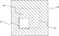
Fig. 4 B is the vertical view of another embodiment of the present invention, and the coldplate 433 that wherein has opening 435 is provided with and is coupling on the semiconductor element 431.Shown in Fig. 4 B, configuration opening 435 exposes a whole angle of semiconductor element 431.In the illustrated embodiment, semiconductor element 431 is thermally coupled to the coldplate 433 in the contact zone, interface 437.Should be appreciated that in the embodiment shown in Fig. 4 B direct clog-free visit is provided to the whole corner of exposing of semiconductor element 431, comprise that the edge that exposes the corner of semiconductor element 431 is used for the probing purpose.In described embodiment, should be appreciated that by rotating semiconductor elements 431 with respect to coldplate 433, the part of the back side needs of semiconductor element 431 is exposed by opening 435, can be implemented to the direct clog-free visit of semiconductor element 431 back side any parts.
Be similar to the embodiment of above introduction, ductile heat conductor can be arranged in the interface contact area 437 between the coldplate 433 and semiconductor element 431.For this reason, the thermal conductivity between semiconductor element 431 and the coldplate 433 increases, and has increased the thermal coupling between semiconductor element 431 and the coldplate 433 thus.By increasing thermal coupling, can reduce the temperature gradient on the semiconductor element 431.
Fig. 4 C is the vertical view of an embodiment more of the present invention with coldplate 473 of opening 475A-D.In the illustrated embodiment, each opening 475A-D of configuration is arranged on the back side of semiconductor element 471A-D correspondence.In described embodiment, semiconductor element 471A-D is included in multi-chip module (MCM) unit.Each semiconductor element 471A-D is thermally coupled to coldplate 473, and heat is delivered to coldplate 473 from each semiconductor element 471A-D thus.Each opening 475A-D is arranged on the corresponding semiconductor element 471A-D, can carry out direct accessible visit to the back side exposed portions serve of each semiconductor element 471A-D thus.Therefore, can in the part that each semiconductor element 471A-D exposes, carry out probing, be used for the silicon probing purpose of Fault Isolation.
Shown in Fig. 4 C, heat is passed contact zone, interface 477A from silicon die 471A and is delivered to coldplate 473.Heat is passed contact zone, interface 477B from semiconductor core 471B and is delivered to coldplate 473.Heat is passed contact zone, interface 477C from semiconductor core 471C and is delivered to coldplate 473.Heat is passed contact zone, interface 477D from semiconductor core 471D and is delivered to coldplate 473.Be similar to the embodiment of above introduction, can be arranged among the contact area 477A-D of interface between the semiconductor element 471A-D and coldplate 473, to increase the thermal coupling between coldplate 473 and each the semiconductor element 471A-D as the ductile heat conductor of indium etc.
Should be appreciated that to the invention is not restricted to have the shape introduced among Fig. 4 A-C and the coldplate of opening, can use coldplate and opening, as long as the semiconductor element cooling semiconductor die that the not obvious coverage of instruction according to the present invention is exposed with other shape.
Fig. 5 is the another embodiment of the method and apparatus of the cooling semiconductor die according to the present invention.In the embodiment show in figure 5, semiconductor element 501 is encapsulated in the C4 encapsulation 503, in C4 encapsulation 503 slots 505 that are contained on the circuit board 507.Be similar to the system that relative Figure 1B introduces, semiconductor element 501 can be worked at the vacuum chamber of the electron beam probing system that is used for silicon debugging and Fault Isolation purpose.
According to the present invention, the coldplate 513 with opening 515 is provided with and is thermally coupled to semiconductor element 501.Opening 515 is arranged on the back side 511 of semiconductor element 501, thus probe unit 509 direct exposed portions serve of visiting semiconductor element 501 back sides 511 without barrier.In one embodiment of the invention, can be arranged between semiconductor element 501 and the coldplate 513, increase the thermal coupling between coldplate 513 and the semiconductor element 501 thus as the ductile heat conductor of indium 517 grades.Therefore, be delivered to coldplate 513 with the heat that specified service speed work produces by indium 517 by semiconductor element 501.
In one embodiment, the temperature control system compatibility of the present invention and present electron beam probing system, wherein cooling block 519 is arranged on the back side of circuit board 507.With reference to figure 5, probe unit 509 probing are installed in the semiconductor element 501 on the circuit board 507.Yet the same with the electron beam probing system of the integrated circuit of many existing probing wire bond package, coldplate 519 is positioned at the back side of circuit board 507.According to the present invention, coldplate 513 transmits conduit 523A by heat and 523B is thermally coupled to cooling block 519.
In one embodiment, heat is transmitted conduit 523A-B and is comprised from coldplate 513 and extend the thermal screw that the opening 525A that passes respectively the circuit board 507 and 525B arrive cooling block 519.In one embodiment, cooling block 519 comprises threaded hole 529A and 529B, to receive screw thread 527A and the 527B that heat is transmitted conduit 523A and 523B respectively.Thus, heat transmission conduit 523A and 523B are thermally coupled to coldplate 513 to cooling block 519, and heat is passed coldplate 513, passed the hot conduit 523A-B arrival cooling block 519 that transmits from semiconductor element 501 thus.
In one embodiment, the hot screw thread that heat is transmitted conduit 523A and 523B comprises excessive respectively head 531A and 531B, and excessive respectively screw thread 527A and 527B.Adopt excessive head 531A and 531B, the amount of surface area that heat is transmitted conduit 523A and 523B thermo-contact coldplate 513 increases, and has reduced thermal resistance thus and has increased thermal conductance.Similarly, adopt excessive screw thread 527A and 527B, the amount of surface area that heat is transmitted conduit 523A and 523B thermo-contact cooling block 519 increases, and has therefore reduced thermal resistance and has increased thermal conductance.
In another embodiment of the present invention, coldplate 513 comprises structure 533A and the 533B on the circuit board 507 that is positioned at coldplate 513, when tightening the hot screw thread of heat transmission conduit 523A and 523B, structure 533A and 533B are tending towards C4 encapsulation 503 is shifted onto in the slot 505 thus.Thus, after the hot screw thread of heat transmission conduit 523A and 523B was tightened, C4 encapsulation 503 can suitably be fixed in the slot 505.In addition, will be appreciated that the hot screw thread that transmits conduit 523A and 523B also can regulate the plane of coldplate 513 and the plane at the back side 511 of semiconductor element 501, further increased the thermo-contact of passing through indium 517 thus.
In one embodiment of the invention, coldplate 513 comprises the copper with the nickel coating.In another embodiment of the present invention, the hot screw thread of heat transmission conduit 523A and 523B also can be by copper production.Should be appreciated that copper is particularly suitable for present application, is because copper is good heat conductor.Yet, should notice that the coldplate 513 that the invention is not restricted to by copper production transmits conduit 523A and 523B with heat, therefore also can use other material according to the present invention, as long as coldplate 513 and heat transmit conduit 523A and 523B has enough thermal conductivity, with cooling semiconductor die 501.In another embodiment of the present invention, cooling agent 521 further assists in removing the heat in the semiconductor element 501 by cooling 519 circulations.
Thus, now introduced the method and apparatus of cooling semiconductor die.Adopt cooling means and the device introduced at present, integrated circuit or MCM unit that C4 installs can carry out in the vacuum chamber of electron beam probing system, are used for silicon debugging and Fault Isolation.At present cooling means of introducing and device also can cool off during based on the test of laser or mechanical probing integrated circuit or the MCM unit in the C4 of vacuum outside work installation.At present the apparatus and method of introducing needn't rely on the heat conduction by encapsulation just can cooling semiconductor die, and the while is covered the circuitry substrate that C4 or MCM unit expose not seriously.In addition, existing temperature control system compatibility in the present invention and the current electron beam probing system, the electron beam probing system encapsulation cooling semiconductor die by each semiconductor element usually.
In above detailed introduction, introduced method and apparatus of the present invention with reference to concrete exemplary embodiment.Yet, obviously can various modifications of memory and change in the spirit and scope of broad of the present invention.Therefore this specification and accompanying drawing are exemplary rather than determinate.
Claims (27)
1. the device of a cooling semiconductor die comprises:
Coldplate with an opening, coldplate is arranged on first of semiconductor element, make coldplate be thermally coupled to semiconductor element at the interface of first surface, heat is delivered to coldplate from semiconductor element thus, the opening of coldplate is arranged on the exposed portions serve of first surface, visits the fundamental region of the exposed portions serve of first surface thus without barrier.
2. according to the device of claim 1, also comprise:
The heat conductor of conformal is arranged between the semiconductor element and coldplate at the interface, and the heat conductor of described conformal forms respectively corresponding surperficial consistent with coldplate and semiconductor element, reduces the thermal resistance between coldplate and the semiconductor element thus.
3. according to the device of claim 2, wherein the heat conductor of conformal is the ductile heat carrier that comprises indium.
4. according to the device of claim 1, wherein coldplate has another opening, coldplate also is arranged on the first surface of another semiconductor element, the first surface of described another semiconductor element another at the interface, coldplate is thermally coupled to described another semiconductor element, heat flows to coldplate from described another semiconductor element thus, another opening of coldplate is arranged on the exposed portions serve of first surface of described another semiconductor element, also can visit the exposed portions serve of another semiconductor element first surface thus without barrier.
5. according to the device of claim 4, wherein semiconductor element and another semiconductor element are included in the multi-chip module.
6. according to the device of claim 1, wherein cooling agent passes the coolant plate circulation with the cooling coolant plate.
7. according to the device of claim 1, wherein semiconductor element is operated on the circuit board, and this device also comprises:
Be arranged on the cooling block on the opposite face of circuit board with respect to semiconductor element; And
The heat that is thermally coupled between coldplate and the cooling block is transmitted conduit, and heat is transmitted conduit from coldplate by heat and is delivered to cooling block thus.
8. according to the device of claim 7, wherein heat is transmitted the screw that conduit comprises thermal coupling coldplate and cooling block.
9. device according to Claim 8, wherein screw comprises the spiral shell head of large size and the screw thread of large size, reduces the thermal resistance between screw and coldplate and the cooling block thus.
10. device according to Claim 8, wherein the configuration screw is clipped on the circuit board semiconductor element.
11. device according to Claim 8, wherein screw comprises copper.
12. according to the device of claim 7, wherein cooling agent passes the circulation of cooling agent piece with cooling cooling agent piece.
13. according to the device of claim 1, wherein coldplate comprises copper.
14. according to the device of claim 1, wherein semiconductor element is included in the control collapse chip and connects in the integrated circuit that (C4) install.
15. the device of a cooling semiconductor die comprises:
Coldplate with opening, this coldplate is arranged on the first surface of semiconductor element, make coldplate be thermally coupled to semiconductor element at the interface of first surface, heat is delivered to coldplate from semiconductor element thus, the opening of coldplate is configured in the exposed portions serve of described first surface, so that visit the fundamental region of the exposed portions serve of described first surface without barrier; And
The heat conductor of conformal is arranged between the semiconductor element and coldplate at the interface, and the heat conductor of described conformal forms respectively corresponding surperficial consistent with coldplate and semiconductor element, reduces the thermal resistance between coldplate and the semiconductor element thus.
16. according to the device of claim 15, wherein the heat conductor of conformal is the ductile heat carrier that comprises indium.
17. according to the device of claim 16, coldplate wherein is set the part first surface is exposed, can visit the exposed portions serve of first surface thus without barrier.
18. according to the device of claim 15, wherein cooling agent passes the coolant plate circulation with the cooling coolant plate.
19. according to the device of claim 15, wherein semiconductor element is operated on the circuit board, device also comprises:
Be arranged on the cooling block on the opposite face of circuit board with respect to semiconductor element; And
The heat that is thermally coupled between coldplate and the cooling block is transmitted conduit, and heat is transmitted conduit from coldplate by heat and is delivered to cooling block thus.
20. according to the device of claim 19, wherein heat is transmitted the screw that conduit comprises thermal coupling coldplate and cooling block.
21. according to the device of claim 20, wherein screw comprises the spiral shell head of large size and the screw thread of large size, reduces the thermal resistance between screw and coldplate and the cooling block thus.
22. according to the device of claim 20, wherein the configuration screw is clipped on the circuit board semiconductor element.
23. according to the device of claim 19, wherein cooling agent passes the circulation of cooling agent piece with cooling cooling agent piece.
24. the device of the semiconductor element of a cooling work on circuit board comprises:
Be arranged on the coldplate on the first surface of semiconductor element, make coldplate be thermally coupled to semiconductor element at the interface of first surface, heat is delivered to coldplate from semiconductor element thus;
Be arranged on the cooling block on the opposite face of circuit board with respect to semiconductor element; And
The heat that is thermally coupled between coldplate and the cooling block is transmitted conduit, and heat is transmitted conduit from coldplate by heat and is delivered to cooling block thus.
25. the device according to claim 24 also comprises:
The heat conductor of conformal is arranged between the semiconductor element and coldplate at the interface, and the heat conductor that forms conformal is consistent with the corresponding apparent surface of coldplate and semiconductor element, reduces the thermal resistance between coldplate and the semiconductor element thus.
26. according to the device of claim 25, wherein the heat conductor of conformal is the ductile heat carrier that comprises indium.
27. according to the device of claim 24, wherein coldplate comprises an opening, the coldplate opening is arranged on the exposed portions serve of first surface, visits the first surface exposed portions serve thus without barrier.
Applications Claiming Priority (2)
| Application Number | Priority Date | Filing Date | Title |
|---|---|---|---|
| US08/856,267 US5923086A (en) | 1997-05-14 | 1997-05-14 | Apparatus for cooling a semiconductor die |
| US08/856,267 | 1997-05-14 |
Publications (2)
| Publication Number | Publication Date |
|---|---|
| CN1263638A CN1263638A (en) | 2000-08-16 |
| CN1154180C true CN1154180C (en) | 2004-06-16 |
Family
ID=25323202
Family Applications (1)
| Application Number | Title | Priority Date | Filing Date |
|---|---|---|---|
| CNB988070995A Expired - Fee Related CN1154180C (en) | 1997-05-14 | 1998-04-14 | Method and apparatus for cooling semiconductor die |
Country Status (7)
| Country | Link |
|---|---|
| US (1) | US5923086A (en) |
| JP (1) | JP4040695B2 (en) |
| KR (1) | KR100381431B1 (en) |
| CN (1) | CN1154180C (en) |
| AU (1) | AU6971898A (en) |
| MY (1) | MY114590A (en) |
| WO (1) | WO1998052223A1 (en) |
Families Citing this family (34)
| Publication number | Priority date | Publication date | Assignee | Title |
|---|---|---|---|---|
| US6043560A (en) * | 1997-12-03 | 2000-03-28 | Intel Corporation | Thermal interface thickness control for a microprocessor |
| US6060777A (en) | 1998-07-21 | 2000-05-09 | Intel Corporation | Underside heat slug for ball grid array packages |
| JP2001015545A (en) * | 1999-07-02 | 2001-01-19 | Shinkawa Ltd | Machine and method for wire bonding |
| US6461891B1 (en) * | 1999-09-13 | 2002-10-08 | Intel Corporation | Method of constructing an electronic assembly having an indium thermal couple and an electronic assembly having an indium thermal couple |
| US6888722B2 (en) * | 1999-12-30 | 2005-05-03 | Intel Corporation | Thermal design for minimizing interface in a multi-site thermal contact condition |
| US6372997B1 (en) | 2000-02-25 | 2002-04-16 | Thermagon, Inc. | Multi-layer structure and method for forming a thermal interface with low contact resistance between a microelectronic component package and heat sink |
| US6761211B2 (en) | 2000-03-14 | 2004-07-13 | Delphi Technologies, Inc. | High-performance heat sink for electronics cooling |
| US6364669B1 (en) * | 2000-07-12 | 2002-04-02 | Advanced Micro Devices, Inc. | Spring contact for providing high current power to an integrated circuit |
| US6317326B1 (en) * | 2000-09-14 | 2001-11-13 | Sun Microsystems, Inc. | Integrated circuit device package and heat dissipation device |
| US7526158B2 (en) * | 2001-02-07 | 2009-04-28 | University Of Rochester | System and method for high resolution optical imaging, data storage, lithography, and inspection |
| US6545346B2 (en) | 2001-03-23 | 2003-04-08 | Intel Corporation | Integrated circuit package with a capacitor |
| US6558169B2 (en) | 2001-03-29 | 2003-05-06 | Intel Corporation | Shunt power connection for an integrated circuit package |
| FR2826508B1 (en) * | 2001-06-20 | 2004-05-28 | Alstom | ELECTRONIC POWER MODULE AND POWER COMPONENT FOR FITTING SUCH A MODULE |
| US6504242B1 (en) | 2001-11-15 | 2003-01-07 | Intel Corporation | Electronic assembly having a wetting layer on a thermally conductive heat spreader |
| US6836014B2 (en) * | 2002-10-03 | 2004-12-28 | Credence Systems Corporation | Optical testing of integrated circuits with temperature control |
| US6771500B1 (en) * | 2003-03-27 | 2004-08-03 | Stmicroelectronics, Inc. | System and method for direct convective cooling of an exposed integrated circuit die surface |
| JP4607445B2 (en) * | 2003-11-04 | 2011-01-05 | 浜松ホトニクス株式会社 | Temperature control device and microscope stand |
| US7616444B2 (en) * | 2004-06-04 | 2009-11-10 | Cooligy Inc. | Gimballed attachment for multiple heat exchangers |
| US7301773B2 (en) * | 2004-06-04 | 2007-11-27 | Cooligy Inc. | Semi-compliant joining mechanism for semiconductor cooling applications |
| US7280363B2 (en) * | 2005-01-21 | 2007-10-09 | Delphi Technologies, Inc. | Apparatus for controlling thermal interface between cold plate and integrated circuit chip |
| US20070125526A1 (en) * | 2005-12-02 | 2007-06-07 | Matsushita Electric Industrial Co., Ltd. | Cooling device for electronic components |
| US7913719B2 (en) | 2006-01-30 | 2011-03-29 | Cooligy Inc. | Tape-wrapped multilayer tubing and methods for making the same |
| WO2007120530A2 (en) | 2006-03-30 | 2007-10-25 | Cooligy, Inc. | Integrated liquid to air conduction module |
| US7715194B2 (en) | 2006-04-11 | 2010-05-11 | Cooligy Inc. | Methodology of cooling multiple heat sources in a personal computer through the use of multiple fluid-based heat exchanging loops coupled via modular bus-type heat exchangers |
| US7834442B2 (en) * | 2007-12-12 | 2010-11-16 | International Business Machines Corporation | Electronic package method and structure with cure-melt hierarchy |
| US20090225514A1 (en) | 2008-03-10 | 2009-09-10 | Adrian Correa | Device and methodology for the removal of heat from an equipment rack by means of heat exchangers mounted to a door |
| US9297571B1 (en) | 2008-03-10 | 2016-03-29 | Liebert Corporation | Device and methodology for the removal of heat from an equipment rack by means of heat exchangers mounted to a door |
| CN102316699B (en) * | 2010-07-07 | 2015-10-14 | 富泰华工业(深圳)有限公司 | Cooling means, the circuit board repair device using this cooling device method and equipment |
| KR101343233B1 (en) * | 2011-11-28 | 2013-12-18 | 삼성전기주식회사 | Power Module Package |
| CN102788945A (en) * | 2012-07-19 | 2012-11-21 | 中国科学院电工研究所 | Universal power semiconductor module fixture |
| JP6048068B2 (en) * | 2012-10-25 | 2016-12-21 | 株式会社島津製作所 | High frequency power supply for plasma and ICP emission spectroscopic analyzer using the same |
| TWI576196B (en) * | 2012-12-05 | 2017-04-01 | Shinkawa Kk | The cooling method of the joining tool cooling device and the joining tool |
| TWI490956B (en) * | 2013-03-12 | 2015-07-01 | Shinkawa Kk | Flip chip bonder and method of flip chip bonding |
| CN108626331B (en) | 2017-03-21 | 2021-03-02 | 株式会社椿本链条 | Tension device |
Family Cites Families (29)
| Publication number | Priority date | Publication date | Assignee | Title |
|---|---|---|---|---|
| US3654528A (en) * | 1970-08-03 | 1972-04-04 | Gen Electric | Cooling scheme for a high-current semiconductor device employing electromagnetically-pumped liquid metal for heat and current transfer |
| JPS5824951B2 (en) * | 1974-10-09 | 1983-05-24 | ソニー株式会社 | Kougakusouchi |
| US4168113A (en) * | 1977-07-05 | 1979-09-18 | American Optical Corporation | Glass lens with ion-exchanged antireflection coating and process for manufacture thereof |
| DE3143336A1 (en) * | 1981-10-31 | 1983-05-19 | SEMIKRON Gesellschaft für Gleichrichterbau u. Elektronik mbH, 8500 Nürnberg | SEMICONDUCTOR RECTIFIER UNIT |
| US4617252A (en) * | 1983-07-01 | 1986-10-14 | Philip A. Hunt Chemical Corporation | Antireflective coatings for use in the manufacture of semi-conductor devices, methods and solutions for making such coatings, and the method for using such coatings to absorb light in ultraviolet photolithography processes |
| GB8328573D0 (en) * | 1983-10-26 | 1983-11-30 | Plessey Co Plc | Diamond heatsink assemblies |
| US4529685A (en) * | 1984-03-02 | 1985-07-16 | Advanced Micro Devices, Inc. | Method for making integrated circuit devices using a layer of indium arsenide as an antireflective coating |
| US4649992A (en) * | 1984-10-05 | 1987-03-17 | Plessey Overseas Limited | Diamond heatsink assemblies |
| US4996589A (en) * | 1987-10-21 | 1991-02-26 | Hitachi, Ltd. | Semiconductor module and cooling device of the same |
| WO1989009958A1 (en) * | 1988-04-08 | 1989-10-19 | Hitachi, Ltd. | Semiconductor module, its cooling system and computer using the cooling system |
| US5001548A (en) * | 1989-03-13 | 1991-03-19 | Coriolis Corporation | Multi-chip module cooling |
| US5106786A (en) * | 1989-10-23 | 1992-04-21 | At&T Bell Laboratories | Thin coatings for use in semiconductor integrated circuits and processes as antireflection coatings consisting of tungsten silicide |
| US5061568A (en) * | 1989-12-20 | 1991-10-29 | Monsanto Company | Solar screening assembly |
| US5146314A (en) * | 1990-03-09 | 1992-09-08 | The University Of Colorado Foundation, Inc. | Apparatus for semiconductor circuit chip cooling using a diamond layer |
| US5070040A (en) * | 1990-03-09 | 1991-12-03 | University Of Colorado Foundation, Inc. | Method and apparatus for semiconductor circuit chip cooling |
| US5004307A (en) * | 1990-04-12 | 1991-04-02 | The Board Of Trustees Of The Leland Stanford Junior University | Near field and solid immersion optical microscope |
| US5000256A (en) * | 1990-07-20 | 1991-03-19 | Minnesota Mining And Manufacturing Company | Heat transfer bag with thermal via |
| JP3249992B2 (en) * | 1990-12-25 | 2002-01-28 | ミノルタ株式会社 | Anti-reflection coating for silicon or germanium substrates |
| EP0512186A1 (en) * | 1991-05-03 | 1992-11-11 | International Business Machines Corporation | Cooling structures and package modules for semiconductors |
| EP0516478A2 (en) * | 1991-05-30 | 1992-12-02 | Nec Corporation | Cooling structure for integrated circuits |
| JP2792304B2 (en) * | 1992-01-22 | 1998-09-03 | 日本電気株式会社 | Cooling device for integrated circuits |
| DE69321501T2 (en) * | 1992-02-10 | 1999-03-04 | Nec Corp., Tokio/Tokyo | Cooling device for components with electronic circuits |
| JP3326721B2 (en) * | 1992-08-04 | 2002-09-24 | 富士通株式会社 | Cooling device for ceramic substrate |
| US5354717A (en) * | 1993-07-29 | 1994-10-11 | Motorola, Inc. | Method for making a substrate structure with improved heat dissipation |
| EP0637078A1 (en) * | 1993-07-29 | 1995-02-01 | Motorola, Inc. | A semiconductor device with improved heat dissipation |
| US5500540A (en) * | 1994-04-15 | 1996-03-19 | Photonics Research Incorporated | Wafer scale optoelectronic package |
| US5418019A (en) * | 1994-05-25 | 1995-05-23 | Georgia Tech Research Corporation | Method for low temperature plasma enhanced chemical vapor deposition (PECVD) of an oxide and nitride antireflection coating on silicon |
| JPH07336077A (en) * | 1994-06-14 | 1995-12-22 | Fujitsu Ltd | Cooling structure of heating-element package |
| JP2926537B2 (en) * | 1994-12-15 | 1999-07-28 | 株式会社日立製作所 | Multi-chip module cooling system |
-
1997
- 1997-05-14 US US08/856,267 patent/US5923086A/en not_active Expired - Lifetime
-
1998
- 1998-04-14 KR KR10-1999-7010524A patent/KR100381431B1/en not_active IP Right Cessation
- 1998-04-14 JP JP54923498A patent/JP4040695B2/en not_active Expired - Fee Related
- 1998-04-14 WO PCT/US1998/007490 patent/WO1998052223A1/en active IP Right Grant
- 1998-04-14 CN CNB988070995A patent/CN1154180C/en not_active Expired - Fee Related
- 1998-04-14 AU AU69718/98A patent/AU6971898A/en not_active Abandoned
- 1998-05-13 MY MYPI98002128A patent/MY114590A/en unknown
Also Published As
| Publication number | Publication date |
|---|---|
| CN1263638A (en) | 2000-08-16 |
| JP2001526838A (en) | 2001-12-18 |
| KR20010012569A (en) | 2001-02-15 |
| MY114590A (en) | 2002-11-30 |
| JP4040695B2 (en) | 2008-01-30 |
| WO1998052223A1 (en) | 1998-11-19 |
| KR100381431B1 (en) | 2003-04-23 |
| AU6971898A (en) | 1998-12-08 |
| US5923086A (en) | 1999-07-13 |
Similar Documents
| Publication | Publication Date | Title |
|---|---|---|
| CN1154180C (en) | Method and apparatus for cooling semiconductor die | |
| US6581388B2 (en) | Active temperature gradient reducer | |
| US7967062B2 (en) | Thermally conductive composite interface, cooled electronic assemblies employing the same, and methods of fabrication thereof | |
| US5396403A (en) | Heat sink assembly with thermally-conductive plate for a plurality of integrated circuits on a substrate | |
| US5367193A (en) | Low cost, thermally efficient, and surface mountable semiconductor package for a high applied power VLSI die | |
| US6404048B2 (en) | Heat dissipating microelectronic package | |
| WO2006020332A1 (en) | Liquid metal thermal interface for an integrated circuit device | |
| US20020185726A1 (en) | Heat pipe thermal management of high potential electronic chip packages | |
| JPH098187A (en) | Method of cooling integrated circuit | |
| JP2000174180A (en) | Semiconductor device | |
| CA2075593A1 (en) | Semiconductor chip module and method for manufacturing the same | |
| US6081028A (en) | Thermal management enhancements for cavity packages | |
| US5146310A (en) | Thermally enhanced leadframe | |
| JP2004200694A (en) | Thermal property enhancement package for integrated circuits | |
| JPS61144855A (en) | Package for semiconductor circuit | |
| JP3193142B2 (en) | Board | |
| JP2011192762A (en) | Power module | |
| CN218827096U (en) | Packaging structure | |
| CN214176010U (en) | Power device and electronic device | |
| US20220344232A1 (en) | Integrated circuit having an enhanced thermal dissipation package | |
| TW202415165A (en) | Embedded thermal and electrical separation circuit board with ceramic substrate and power transistor which has a high-power component and a heat dissipation ceramic block embedded together in a printed circuit board to improve the over thermal conductivity efficiency | |
| TW202415166A (en) | Embedded thermoelectric separation circuit board with ceramic substrate and power transistor to make an overall thermal conductivity better, and make an overall thickness thinner while maintaining proper thermal and electrical separation functions by changing a thickness of a heat dissipation ceramic block | |
| JP2806345B2 (en) | Multi-chip module | |
| JPS612350A (en) | Semiconductor integrated circuit device | |
| JPH0547967A (en) | Semiconductor chip module |
Legal Events
| Date | Code | Title | Description |
|---|---|---|---|
| C06 | Publication | ||
| PB01 | Publication | ||
| C10 | Entry into substantive examination | ||
| SE01 | Entry into force of request for substantive examination | ||
| C14 | Grant of patent or utility model | ||
| GR01 | Patent grant | ||
| C17 | Cessation of patent right | ||
| CF01 | Termination of patent right due to non-payment of annual fee |
Granted publication date: 20040616 Termination date: 20100414 |