Semiconductor integrated circuit
Invention field
The present invention relates to a kind of semiconductor integrated circuit, the semiconductor integrated circuit of low-power consumption especially is used to prolong the battery life of portable electronic instrument etc.
Background technology
In recent years,, can use the longer time, just require to make semiconductor integrated circuit (LSI) to realize low power consumption in order to make internal battery along with the progress and the development of portable instrument.As the effective method of realizing low power consumption, the method for reduction operating voltage etc. is for example arranged.That is, because electrical power equals the product of voltage and current, so, by reducing operating voltage, just voltage and current all can be reduced, like this, the effect that has usually square.
But the MOSFET (MOS field-effect transistor) that constitutes LSI has the slack-off character of action degradation speed when supply voltage reduces.Supply voltage can not reduce threshold voltage without a moment's thought even this character results from reduction.Because if reduce threshold voltage, the leakage current when MOSFET ends will increase, and increase power consumption on the contrary.In order to address this problem, be to adopt following method in the past.
Fig. 7 is that for example the spy opens the low voltage operating circuit of the disclosed existing so-called MT-CMOS of flat 7-212218 communique (Multi-threshold CMOS).Among the figure, 1,2 and 5 is p channel mosfets, and 3,4 and 6 is n channel mosfets.Set the absolute value of the threshold voltage of p channel mosfet 1,2 to such an extent that be lower than the absolute value of the threshold voltage of p channel mosfet 5, simultaneously, set the absolute value of the threshold voltage of n channel mosfet 3,4 to such an extent that be lower than the absolute value (after, suppose that " threshold voltage " is meant its absolute value) of the threshold value of n channel mosfet 6.And these MOSFET1~4 constitute the combinational circuit 11 of two input NOT-AND gates.In addition, p channel mosfet 5 is connected between supply voltage 12 and the imaginary power line 9, and control signal CSB1 is input to its grid, and n channel mosfet 6 is connected between imaginary ground wire 10 and the ground 13, and control signal CS1 is input to its grid.
Below, its action is described.
When making combinational circuit 11 actions of this two inputs NOT-AND gate, make control signal CS1 become high level, simultaneously, making its inversion signal is that control signal CSB1 becomes low level.Therefore, p channel mosfet 5 and n channel mosfet 6 all become conducting state, and imaginary power line 9 rises to the voltage level V of supply voltage 12
DD, on the other hand, imaginary ground wire 10 is reduced to the voltage level V on ground 13
GNDAs a result, this combinational circuit 11 carries out common NAND action.At this moment, owing to set the threshold voltage (absolute value) of MOSFET1~4 low, so, at the voltage V of supply voltage 12
DDAlso can high speed motion during for low-voltage.
When combinational circuit 11 is not worked, make control signal CS1 become low level, making its inversion signal is that control signal CSB1 becomes high level.At this moment, p channel mosfet 5 and n channel mosfet 6 all end, and imaginary power line 9 and imaginary ground wire 10 be deenergization voltage 12 and ground 13 respectively.At this moment, owing to all set the threshold voltage (absolute value) of p channel mosfet 5 and n channel mosfet 6 to such an extent that be higher than MOSFET1~4, so, can get drain current suppressing very little.
Usually, the voltage between the gate-source of MOSFET is less than the zone of threshold voltage, and the leakage current between source drain is pressed exponential function with grid voltage to be increased.Therefore, when combinational circuit 11 is not worked, voltage difference is arranged, just can reduce leakage current significantly by making MOSFET1~4 and MOSFET5,6 threshold voltage.As an example, Fig. 7 shows the situation that combinational circuit 11 is two input NOT-AND gates, and still, no matter in the circuit of which type of kind that constitutes LSI and scale, same discussion is all set up.
Because the semiconductor integrated circuit of existing low-voltage action type constitutes in a manner described, so, as two input NOT-AND gates, under the situation of the combinational circuit that determines by output and input combination, can normally work, but, under the situation of sequential circuit, have problems such as misoperation takes place with the function of storing the state before keeping.
As an example of this sequential circuit, figure 8 illustrates the figure of the so-called latch cicuit that the input and output of 2 inverters are formed by connecting mutually across.Among the figure, the 14, the 15th, the p channel mosfet, the 16, the 17th, the n channel mosfet, they all have low threshold voltage (absolute value).The 5th, the p channel mosfet, the 6th, the n channel mosfet, their threshold voltage (absolute value) is all high.Constitute sequential circuit 20 by these MOSFET14~17, node 18,19 forms a pair of storage and keeps node, and when a node was high level, another node became low level, thereby can keep the value imported.
Below, its action is described.
Be high level at CS1, when simultaneously CSB1 becomes under the low level state sequential circuit 20 actions, the value of the data that write is normally kept, and because the threshold voltage of p channel mosfet 14,15 and n channel mosfet 16,17 is all low, so, can write at high speed and read to node 18,19.
But when being failure to actuate, CS1 is that low level and CSB1 become high level, and leakage current reduces, at this moment since MOSFET14~17 by the time leakage current greater than MOSFET5,6 by the time leakage current, so, can not keep the data of node 18,19.Because, for example suppose that node 18 is low level for high level, node 19, then p channel mosfet 15 in MOSFET14~17 and n channel mosfet 16 are for ending, and other 2 for conducting, but, because flow through the influence of the leakage current of p channel mosfet 15 and n channel mosfet 16, the level of the node 18 of high level will reduce, the level of low level node 19 will rise.Till this process will last till that the level of node 18,19 equates, its result, the data that keep losing.Like this, in the semiconductor integrated circuit of existing low-voltage action type, there is the problem of the data of losing sequential circuit.
Summary of the invention
The present invention is motion in order to address the above problem, and purpose is to provide the maintenance data that can not destroy sequential circuit, utilize the reducing of leakage current of the circuit of being failure to actuate and realize the semiconductor integrated circuit of low power consumption.
According to a first aspect of the invention, provide a kind of semiconductor integrated circuit, it is characterized in that having: power voltage line; Earth connection; Switch element is connected with earth connection with described power voltage line respectively; The combinational circuit that is connected with this switch element; Sequential circuit is connected with earth connection and comprises that with described power voltage line at least more than one P-slot field-effect transistor with back grid and at least more than one have the N-slot field-effect transistor of back grid; And control unit, by the variable positive voltage generator of the threshold voltage that makes the described P-slot field-effect transistor in the said sequence circuit by above-mentioned back grid with by above-mentioned back grid the variable negative-voltage generator of threshold voltage of the described N-slot field-effect transistor in the said sequence circuit is constituted.
Preferably, in described combinational circuit, include at least more than one combinational circuit P-slot field-effect transistor and at least more than one combinational circuit N-slot field-effect transistor, in switch element, include switch P-slot field-effect transistor and switch N-slot field-effect transistor, and the absolute value of the threshold voltage of above-mentioned switch usefulness P-slot field-effect transistor is than the absolute value height of combinations thereof circuit with the threshold voltage of P-slot field-effect transistor, and above-mentioned switch is used the absolute value height of the threshold voltage of N-slot field-effect transistor than combinations thereof circuit with the absolute value of the threshold voltage of N-slot field-effect transistor.
Perhaps, in described combinational circuit, include at least more than one combinational circuit P-slot field-effect transistor and at least more than one combinational circuit N-slot field-effect transistor, in switch element, include switch P-slot field-effect transistor and switch N-slot field-effect transistor, and the combinations thereof circuit equates with the absolute value of above-mentioned switch with the threshold voltage of P-slot field-effect transistor with the absolute value of the threshold voltage of P-slot field-effect transistor, the combinations thereof circuit equates with the absolute value of above-mentioned switch with the threshold voltage of N-slot field-effect transistor with the absolute value of the threshold voltage of N-slot field-effect transistor, when the combinations thereof circuit is in cut-off state, be input to above-mentioned switch and be higher than supply voltage, and be input to above-mentioned switch and be lower than earthed voltage with the control signal of the grid of N-slot field-effect transistor with the control signal of the grid of P-slot field-effect transistor.
Preferably, described semiconductor integrated circuit comprises a plurality of combinations thereof circuit that are connected respectively by a plurality of switch elements and above-mentioned power voltage line and described earth connection, with above-mentioned power voltage line and described earth connection a plurality of said sequence circuit that are connected respectively and the control unit that is connected with above-mentioned each sequential circuit respectively; Above-mentioned each switch element and each control unit also have the generation voltage higher than supply voltage the 1st a common stepup transformer, produce the 1st a common reducing transformer of the voltage lower than earthing potential, above-mentioned each switch element also has rp unit that is connected with above-mentioned the 1st stepup transformer and the noninverting unit that is connected with above-mentioned the 1st reducing transformer.
Wherein, above-mentioned the 1st stepup transformer is connected with the positive voltage generator, and above-mentioned the 1st reducing transformer is connected with negative-voltage generator, and above-mentioned positive voltage generator and above-mentioned negative-voltage generator comprise 1 multiplexer respectively.
In described semiconductor integrated circuit, above-mentioned a plurality of combinational circuits and above-mentioned a plurality of sequential circuit are formed as 1 logical circuit, and above-mentioned 1 logical circuit, above-mentioned the 1st stepup transformer, above-mentioned the 1st reducing transformer are formed in the same integrated circuit; Use above-mentioned the 1st stepup transformer and above-mentioned the 1st reducing transformer, by above-mentioned power voltage line and above-mentioned earth connection, drive each the above-mentioned switch element that is connected with the combinations thereof circuit, and control constitutes the work of the above-mentioned field-effect transistor of said sequence circuit.
Wherein, the integrated circuit with above-mentioned stepup transformer and reducing transformer is made of dynamic random access memory.
Description of drawings
Fig. 1 is the circuit structure diagram of the semiconductor integrated circuit of the embodiment of the invention 1.
Fig. 2 is the circuit structure diagram of the semiconductor integrated circuit of the embodiment of the invention 2.
Fig. 3 is the circuit structure diagram of the semiconductor integrated circuit of the embodiment of the invention 3.
Fig. 4 is the circuit structure diagram of the semiconductor integrated circuit of the embodiment of the invention 4.
Fig. 5 is the circuit structure diagram of the semiconductor integrated circuit of the embodiment of the invention 5.
Fig. 6 is the circuit structure diagram of the semiconductor integrated circuit of the embodiment of the invention 6.
Fig. 7 is the circuit structure diagram of the low-voltage actuating circuit of existing MT-CMOS.
Fig. 8 is the circuit structure diagram of existing latch cicuit.
Embodiment
Below, embodiments of the invention are described.
Embodiment 1.
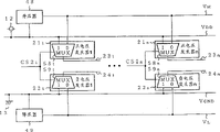
Fig. 1 is the figure of semiconductor integrated circuit of the low-voltage action type of the expression embodiment of the invention 1, among the figure, and the 1, the 2nd, p channel mosfet, the 5th, p channel mosfet, the 3, the 4th, n channel mosfet, the 6th, n channel mosfet, the 23, the 24th, back grid node.Here, the absolute value of the threshold voltage of p channel mosfet 1,2 set be lower than p channel mosfet 5 the absolute value of threshold voltage, simultaneously, the absolute value of the threshold voltage of n channel mosfet 3,4 is set to such an extent that be lower than the absolute value (after, suppose that " threshold voltage " is meant its absolute value) of the threshold voltage of n channel mosfet 6.And, the combinational circuit 11 of these MOSFET1~4 configuration examples as two input NOT-AND gates, MOSFET5,6 constitutes switch element.At this moment, p channel mosfet 5 is connected between supply voltage 12 and the imaginary power line 9, and control signal CSB1 is input to its grid.In addition, n channel mosfet 6 is connected between imaginary ground wire 10 and the ground 13, and control signal CS1 is input to its grid.
On the other hand, the 14, the 15th, the p channel mosfet, the 16, the 17th, the n channel mosfet, they constitute sequential circuit 20.In addition, the back grid of positive voltage generator 21, negative-voltage generator 22 and MOSFET14~17 constitutes control unit with node 23,24.These MOSFET14~17 are made of the low transistor of the absolute value of threshold voltage, and node 18,19 forms a pair of storage and keeps node.At this moment, the back grid current potential VC1 of p channel mosfet 14,15 is connected with the output of positive voltage generator 21, the back grid current potential VD1 of n channel mosfet 16,17 is connected with the output of negative-voltage generator 22.
Below, its action is described.
When making combinational circuit 11 actions, make control signal CS1 become high level, simultaneously, making its inversion signal is that control signal CSB1 becomes low level.Like this, p channel mosfet 5 and n channel mosfet 6 all become conducting state, and imaginary power line 9 rises to the potential level V of supply voltage 12
DD, on the other hand, imaginary ground wire 10 is reduced to the level V on ground 13
GNDAs a result, the combinational circuit 11 of two such input NOT-AND gates just carries out common NAND action.At this moment, because the threshold voltage (absolute value) of MOSFET1~4 is set lowly, so, even when the voltage of supply voltage 12 is low-voltage, also can carry out action at a high speed with low-power consumption.
When combinational circuit 11 is failure to actuate, make control signal CS1 become low level, making its inversion signal is that control signal CSB1 becomes high level.At this moment, p channel mosfet 5 and n channel mosfet 6 all end, and imaginary power line 9 and imaginary ground wire 10 be deenergization voltage 12 and ground 13 respectively.Here, owing to set the threshold voltage (absolute value) of p channel mosfet 5 and n channel mosfet 6 to such an extent that all be higher than MOSFET1~4, so, can get drain current suppressing very little.
On the other hand, for sequential circuit 20, the control signal CS2 of Input Control Element becomes high level when action, because the effect of positive voltage generator 21, the back grid current potential VC1 of p channel mosfet 14,15 becomes mains voltage level V
DD, simultaneously, because the effect of negative-voltage generator 22, the back grid current potential VD1 of n channel mosfet 16,17 becomes earth potential level V
GNDTherefore, at this moment, sequential circuit 20 can carry out common storage and keep action.At this moment, because the absolute value of the threshold voltage of the p channel mosfet 14,15 of formation sequential circuit 20 and n channel mosfet 16,17 is all low, so, can carry out writing and reading of data at high speed to node 18,19.In addition, when sequential circuit 20 was failure to actuate, CS2 became low level, and the output VC1 of positive voltage generator 21 also is higher than supply voltage V
DD, the output VD1 of negative-voltage generator 22 is lower than earth potential V
GNDValue.As a result, because the back grid current potential VC1 of p channel mosfet 14,15 is higher than supply voltage 12, so, its threshold voltage raises, in addition, because the back grid current potential VD1 of the back grid of n channel mosfet 16,17 is lower than supply voltage 12, so threshold voltage still raises.Therefore, can reduce the leakage current that flows to ground 13 from the supply voltage 12 of sequential circuit 20.
As mentioned above,, when sequential circuit 20 is failure to actuate, thereby improve its threshold voltage, just can obtain to reduce leakage current, not destroy the effect that storage keeps the data of node and reduces power consumption by the back grid current potential that changes low threshold mos FET according to present embodiment 1.In addition, because the threshold value of the MOSFET that uses in combinational circuit 11 and sequential circuit 20 is low, so having when action also can be at a high speed and the effect that writes with low power and read.In present embodiment 1, be that control signal CS1 is described as different signals with CSB1, still, also can realize same action even both are same signals, thereby can obtain same effect.
Embodiment 2.
Fig. 2 is the figure of semiconductor integrated circuit of the low-voltage action type of the expression embodiment of the invention 2, among the figure, because the structure of sequential circuit 20 is identical with embodiment 1 with action, so, same section is marked with identical symbol, and omission repeat specification.In embodiment 2, the leakage current when combinational circuit 11 is failure to actuate reduces the MOSFET5 of usefulness, 6 threshold voltage settings is and the same low threshold voltage in other MOSFET1~4.
Below, its action is described.
In present embodiment 2, when combinational circuit 11 is failure to actuate, be by control signal CS1 is become than ground level V
GNDLow current potential, simultaneously CSB1 is become than supply voltage V
DDHigh current potential realizes reducing leakage current.Otherwise, because the threshold value of the MOSFET of the threshold value of the MOSFET of formation switch element and formation combinational circuit is same magnitude, so, will between power supply and ground leakage current take place, thereby will increase the power consumption of entire circuit like that.Therefore, if constitute in the manner described above, not only do not use MOSFET just can obtain the effect identical, and comprise that the employed MOSFET5 of switch element, 6 can make whole threshold values reductions with embodiment 1 with multiple threshold voltage.Therefore, when making semiconductor integrated circuit, can reduce the mask number, owing to can reduce the worker ordinal number, so, can reduce manufacturing cost.
Embodiment 3.
Fig. 3 is the block diagram of the circuit block that will be made of a plurality of combinational circuits and sequential circuit respectively when being applied to large scale integrated circuit (LSI) of the expression embodiment of the invention 3, among the figure, and 11
1~11
mBe the piece of combinational circuit, possess input control signal CSB1 respectively
1~CSB1
mP channel mosfet 5
1~5
mWith input control signal CS1
1~CS1
mN channel mosfet 6
1~6
mOn the other hand, 20
1~20
nBe the piece of sequential circuit, possess input CS2 respectively
1~CS2
nPositive voltage generator 21
1~21
n, negative-voltage generator 22
1~22
n, back grid is with node (control unit) 23
1~23
nWith 24
1~24
nOther structures are because identical with above-mentioned embodiment shown in Figure 22, so, identical part is marked with identical symbol, and omits repeat specification.
Piece 11 at combinational circuit
1~11
mIn, p channel mosfet 5
1~5
mHas low threshold value, according to control signal CSB1
1~CSB1
mCarry out the action identical with the p channel mosfet 5 of embodiment 2, in addition, n channel mosfet 6
1~6
mAlso be low threshold value, according to control signal CS1
1~CS1
mCarry out the action identical with the n channel mosfet 6 of embodiment 2.In addition, the positive voltage generator 21
1~21
nCarry out the action identical, respectively according to control signal CS2 with the positive voltage generator 21 of embodiment 1
1~CS2
nControl sequence circuit 20
1~20
nThe back grid of p channel mosfet with node 23
1~23
nOn the other hand, at the piece 20 of sequential circuit
1~20
nIn, negative-voltage generator 22
1~22
nAlso carry out the action identical, respectively according to control signal CS2 with the negative-voltage generator 22 of embodiment 1
1~CS2
nControl sequence circuit 20
1~20
nThe back grid of n channel mosfet with node 23
1~23
nControl signal CSB1
1~CSB1
m, CS1
1~CS1
mWith control signal CS2
1~CS2
nCan work independently.
Below, its action is described.
By with control signal CSB1
1~CSB1
m, CS1
1~CS1
mImport the piece 11 of combinational circuit respectively independently
1~11
m, the piece 11 of combinational circuit
1~11
mAction independently respectively, on the other hand, same passing through with control signal CS2
1~CS2
nAlso distinguish the piece 20 of input sequence circuit independently
1~20
n, make the piece 20 of sequential circuit
1~20
nAction independently respectively.
As mentioned above, according to present embodiment 3, owing to can control the action of the sequential circuit when being failure to actuate independently to the piece of each sequential circuit, so, can individually control and reduce leakage current so that can not destroy by each storage maintenance data that node kept, and owing to do not use the MOSFET with multiple threshold value, so, can reduce the worker ordinal number thereby can reduce mask number etc.Therefore, thus the semiconductor integrated circuit that can obtain to reduce manufacturing cost and reduce finished productization when standby etc. not the leakage current of working portion can suppress the effect of electric power consumption.Here, be that the semiconductor integrated circuit with Fig. 2 is that the basis describes, still, also can be based on the semiconductor integrated circuit of Fig. 1.
Embodiment 4.
Fig. 4 is the figure of circuit structure of the semiconductor integrated circuit of the expression embodiment of the invention 4, is to use stepup transformer and reducing transformer generation control signal CSB1
1~CSB1
mAnd CS1
1~CS1
mSituation.Among the figure, the 48th, produce the stepup transformer (the 1st stepup transformer) of the voltage higher than supply voltage, the 49th, produce the reducing transformer (the 1st reducing transformer) of the voltage lower, 50 than earthing potential
1~50
mBe buffer circuit with inverter functionality of control signal BE1~BEm, 51
1~51m
mBe to have control signal BE
1~BE
mThe buffer circuit of noninverting function, buffer circuit 50
1~50
mWith noninverting buffer circuit 51
1~51
mConstitute rp unit and noninverting unit respectively.V
H, V
LBe respectively to have than supply voltage V
DDThe output of the stepup transformer 48 of high current potential and having than earth potential V
GNDThe output of the reducing transformer 49 of low current potential.In addition, anti-phase buffer circuit 50
1~50
mRespectively with power supply and ground and node ND1
1With node ND2
1..., node ND1
mWith node ND2
mConnect noninverting buffer circuit 51
1~51
mRespectively with power supply and ground and node ND3
1With node ND4
1..., node ND3
mWith node ND4
mConnect.Control signal BE
1~BE
mBe that the control signal that is used to control to the combinational circuit input is CSB1
1~and CS1
1..., CSB1
mAnd CS1
mSignal.Other structures are identical with above-mentioned embodiment shown in Figure 33, so, identical part is marked with identical symbol, and omits repeat specification.
Below, its action is described.
With 1 combinational circuit 11 in m shown in Figure 3 the combinational circuit piece
1Be example, control signal BE when action
1Become high level.At this moment, at buffer circuit 50
1With 51
1In, CSB1
1And CS1
1Become ground level V respectively
GNDWith mains voltage level V
DD, carry out the action of explanation in embodiment 3.Control signal BE when being failure to actuate
1Become low level, at this moment, CSB1
1By anti-phase buffer circuit 50
1Carry out anti-phasely, become and have than supply voltage V
DDThe node ND1 of high current potential
1Current potential V
H, in addition, CS1
1By noninverting buffer circuit 51
1Do not carry out anti-phasely, become node ND4 with current potential lower than ground level
1Current potential V
LLike this, just with in embodiment 3 explanation the same, can reduce combinational circuit piece 11
1Leakage current.Equally, for buffer circuit 50
m, 51
m, also according to control signal BE
mCarry out above-mentioned action.
As mentioned above, according to present embodiment 4, only in anti-phase buffer circuit and noninverting buffer circuit, added simple circuit such as stepup transformer and reducing transformer, leakage current in the time of just can further reducing combinational circuit and do not work, so, have and can further reduce the not power consumption that causes of the leakage current of working portion of semiconductor integrated circuit.Embodiment 4 also can boost with in reduction voltage circuit is arranged on the chip identical with the circuit that is made of combinational circuit shown in the embodiment 3 and sequential circuit above-mentioned, like this, just can dwindle the size of the chip of bearing semiconductor integrated circuit.
Embodiment 5.
Fig. 5 is the figure of circuit structure of the semiconductor integrated circuit of the expression embodiment of the invention 5, among the figure, and 58
1~58
nBe respectively to constitute positive voltage generator 21
1~21
nMulti-channel conversion circuit (MUX), 59
1~59
nBe respectively to constitute negative-voltage generator 22
1~22
nMulti-channel conversion circuit (MUX).Other structures are identical with embodiment 4, so, identical part is marked with identical symbol, and omits repeat specification.
Below, its action is described.
For example, at the sequential circuit 20 of Fig. 3
1Control signal CS2 during action
1Become high level, at multi-channel conversion circuit 58
1In, select supply voltage V
DDTo back grid node 23
1Output is at multi-channel conversion circuit 59
1In, earth potential V
GNDTo back grid node 24
1Output.Control signal CS2 when being failure to actuate
1Become low level, at multi-channel conversion circuit 58
1In, select the current potential V higher than supply voltage
HTo back grid node 23
1Output is at multi-channel conversion circuit 59
1In, select the current potential V lower than earth potential
LTo back grid node 24
1Output.Like this, just, can realize the action identical with embodiment 3.
As mentioned above, according to present embodiment 5, because the multi-channel conversion circuit of simple and inexpensive is applied to positive and negative voltage generator, so, even when sequential circuit is not worked, also can reduce leakage current, thereby can not destroy the maintenance data of sequential circuit.Therefore, have with low manufacturing cost and reduce the be failure to actuate effect of power consumption of part of semiconductor integrated circuit.
In embodiment 5, supposition stepup transformer (stepup transformer that is made of simple multi-channel conversion circuit) 48 and reducing transformer (reducing transformer that is made of simple multi-channel conversion circuit) 49 describe with the identical of embodiment 4, but, if suppose that they are different and can set output voltage individually, can also realize reducing more subtly leakage current.In addition, also the circuit that is made of positive and negative voltage generator shown in the present embodiment 5 can be arranged in the chip identical with the circuit that is made of combinational circuit and sequential circuit shown in the embodiment 3, like this, just, can dwindle the size of the chip of bearing semiconductor integrated circuit.
Embodiment 6.
Fig. 6 is the figure of circuit structure of the semiconductor integrated circuit of the expression embodiment of the invention 6, among the figure, the 62nd, be the high integrated MOS RAM that the stored information of representative need refresh for example with flash memory, dynamic random access memory (DRAM), the 63rd, logical circuit, and be the so-called mixed type semiconductor integrated circuit of storage part and logic section mixed type.The logical circuit that is made of combinational circuit and sequential circuit of the structure of logical circuit and embodiment 3 is identical.In high integrated MOS RAM, carry out and must circuit be moved refresh activity well, so, stepup transformer 48 and reducing transformer 49 are set usually, if with their output V in inside
H, V
LBe applied to logical circuit 63, can as embodiment 3, move.
As mentioned above, according to present embodiment 6, owing to can effectively utilize stepup transformer and the reducing transformer that is arranged on DRAM inside, so, can dwindle the area that adjunct circuit occupies, therefore, can suppress the increase of the component number of hardware.As a result, the leakage current of working portion can reduce power consumption thereby not only can reduce in the semiconductor integrated circuit not, but also can dwindle the chip size of the conductor integrated circuit device of making, thereby can reduce manufacturing cost.
As mentioned above, according to the present invention, make the 1st of sequential circuit use owing to have control module The threshold voltage of field-effect transistor is variable, so, when moving, sequential circuit can make the 1st Can be to the storage that in this sequential circuit, forms thereby the threshold voltage of field-effect transistor reduces Keep node to carry out at high speed writing and reading of data with low-power consumption, add at sequential circuit motionless By improving the threshold voltage of the 1st field-effect transistor, can reduce leakage current when doing, like this, Just has the effect that data that the storage of making keeps node to keep can not be destroyed and disappear.
In addition, switch element consists of can make itself and other circuit part when combinational circuit is failure to actuate Divide to disconnect, so, the leakage current of combinational circuit can be reduced.
According to the present invention, the 1st field-effect transistor that consists of sequential circuit has back grid, institute With, control module was not controlled its current potential by back grid when sequential circuit was not worked, and improved the 1st effect Answer transistorized threshold value, thereby can reduce leakage current, like this, can prevent that just storage from keeping node The data corruption that keeps and disappearance, and can realize low power consumption.
According to the present invention, the control module that is connected with sequential circuit comprises positive voltage generator and negative electricity Press generator, so the positive voltage generator and the negative voltage that utilize input to be connected with back grid take place The control signal of device is high level or low level, can make the p raceway groove and the n that consist of sequential circuit The threshold value of the 1st field-effect transistor of raceway groove is variable. Therefore, in sequential circuit when action, is with low threshold Value makes transistor action, so, can carry out zero access and can reduce power consumption, in addition On the one hand, when sequential circuit is failure to actuate, because the transistorized threshold value of p raceway groove is higher than Supply voltage makes the transistorized threshold value of n raceway groove be lower than earth potential simultaneously, so, can reduce The leakage current of circulation from the power supply of sequential circuit to ground like this, just has the storage of making and keeps node institute The effect that the data that keep do not disappear.
In addition, if use the transistor with above-mentioned back grid to consist of sequential circuit, use threshold value Little transistor just can consist of, so, follow the mask number to reduce, can reduce process number, from And can reduce manufacturing cost, and, owing to can dwindle the conductor integrated circuit device of making Chip size, so, can improve product percent of pass.
According to the present invention, the threshold voltage of the 2nd field-effect transistor that combinational circuit uses compares switch The threshold voltage of the 3rd field-effect transistor that the unit uses is little, so, only suppress to be input to combination The level of the control signal on the grid of circuit just can carry out at high speed with low-power consumption logic and move Do.
According to the present invention, threshold voltage and the switch of the 2nd field-effect transistor that combinational circuit uses The threshold voltage of the 3rd field-effect transistor that the unit uses about equally, the 3rd field-effect transistor When being in cut-off state, in the transistor of the transistor of supply voltage one side and ground one side, make it Voltage reversal biasing between gate-source is so the transistor that above-mentioned switch element uses is also passable Use transistor and the little transistor of threshold value that combinational circuit uses. Therefore, because at 1 half Do not mix in the conductor integrated circuit and have the transistor with multiple threshold value, so, can reduce and cover The film number makes manufacturing process simple and easy, thereby can reduce manufacturing cost.
According to the present invention, consist of combinational circuit piece, a plurality of orders owing to constitute a plurality of combinational circuits Circuit consists of the sequential circuit piece, and switch element is connected respectively with each circuit block, makes institute's sequential circuit Variable control module and each circuit block of threshold voltage of the 1st field-effect transistor connect respectively Connect, so, can consider that many conditions such as the power consumption of semiconductor integrated circuit and access speed are more smart Carefully suppress leakage current, thereby can make the storage of sequential circuit keep data not disappear.
According to the present invention, during owing to control signal process rp unit and noninverting unit, at power supply One side and ground one side, the 1st stepup transformer and reducing transformer respectively the gauge tap unit have the Current potential between the gate-source of 3 field-effect transistors, so, mutual reverse bias can be become. Like this, just can reduce the leakage current of combinational circuit by adding simple circuit, so, can fall Low-power consumption.
According to the present invention, the control unit that is connected with sequential circuit possesses stepup transformer that is connected with the positive voltage generator that is made of simple multi-channel conversion circuit and the reducing transformer that is connected with the negative-voltage generator that is made of simple multi-channel conversion circuit, positive voltage generator and negative-voltage generator, so, in the time of can setting sequential circuit and not working through the control signal of multi-channel conversion circuit, by can reduce the leakage current of sequential circuit behind the back grid effectively in stepup transformer one side and reducing transformer one side.Therefore, only merely additional cheap circuit just can further reduce the power consumption of circuit and make storage keep data not disappear.
According to the present invention, stepup transformer that stepup transformer and reducing transformer and switch element comprised and reducing transformer that control unit comprised constitute independently, so, can individually set output voltage, thereby can reduce leakage current more subtly, like this, just, can realize the low power consumption of the conductor integrated circuit device integral body made.
According to the present invention, the circuit that will comprise stepup transformer and reducing transformer combines with the logical circuit that comprises combinational circuit and sequential circuit, so, if the stepup transformer and the reducing transformer of integrated circuit are used in this logical circuit, just can omit the setting of adjunct circuit, so, can dwindle the chip size of conductor integrated circuit device integral body.And because chip size reduces, the manufacturing cost of per 1 disk also reduces.
According to the present invention, the integrated circuit that possesses stepup transformer and reducing transformer is made of dynamic random access memory (DRAM), so, can make the hybrid circuit of logical circuit and DRAM, usually, DRAM possesses in order to carry out refresh activity etc. and has stepup transformer and reducing transformer, so, can be designed as they are used in the action of logical circuit.Therefore, can not cause the component number increase and dwindle the area that whole hybrid circuit occupies.