JP3732914B2 - Semiconductor device - Google Patents
Semiconductor device Download PDFInfo
- Publication number
- JP3732914B2 JP3732914B2 JP04523597A JP4523597A JP3732914B2 JP 3732914 B2 JP3732914 B2 JP 3732914B2 JP 04523597 A JP04523597 A JP 04523597A JP 4523597 A JP4523597 A JP 4523597A JP 3732914 B2 JP3732914 B2 JP 3732914B2
- Authority
- JP
- Japan
- Prior art keywords
- voltage
- circuit
- power supply
- mosfet
- well
- Prior art date
- Legal status (The legal status is an assumption and is not a legal conclusion. Google has not performed a legal analysis and makes no representation as to the accuracy of the status listed.)
- Expired - Fee Related
Links
Images


Classifications
-
- H—ELECTRICITY
- H01—ELECTRIC ELEMENTS
- H01L—SEMICONDUCTOR DEVICES NOT COVERED BY CLASS H10
- H01L21/00—Processes or apparatus adapted for the manufacture or treatment of semiconductor or solid state devices or of parts thereof
- H01L21/70—Manufacture or treatment of devices consisting of a plurality of solid state components formed in or on a common substrate or of parts thereof; Manufacture of integrated circuit devices or of parts thereof
- H01L21/77—Manufacture or treatment of devices consisting of a plurality of solid state components or integrated circuits formed in, or on, a common substrate
- H01L21/78—Manufacture or treatment of devices consisting of a plurality of solid state components or integrated circuits formed in, or on, a common substrate with subsequent division of the substrate into plural individual devices
- H01L21/82—Manufacture or treatment of devices consisting of a plurality of solid state components or integrated circuits formed in, or on, a common substrate with subsequent division of the substrate into plural individual devices to produce devices, e.g. integrated circuits, each consisting of a plurality of components
- H01L21/822—Manufacture or treatment of devices consisting of a plurality of solid state components or integrated circuits formed in, or on, a common substrate with subsequent division of the substrate into plural individual devices to produce devices, e.g. integrated circuits, each consisting of a plurality of components the substrate being a semiconductor, using silicon technology
- H01L21/8232—Field-effect technology
-
- G—PHYSICS
- G11—INFORMATION STORAGE
- G11C—STATIC STORES
- G11C5/00—Details of stores covered by group G11C11/00
- G11C5/14—Power supply arrangements, e.g. power down, chip selection or deselection, layout of wirings or power grids, or multiple supply levels
- G11C5/145—Applications of charge pumps; Boosted voltage circuits; Clamp circuits therefor
- G11C5/146—Substrate bias generators
-
- G—PHYSICS
- G11—INFORMATION STORAGE
- G11C—STATIC STORES
- G11C5/00—Details of stores covered by group G11C11/00
- G11C5/14—Power supply arrangements, e.g. power down, chip selection or deselection, layout of wirings or power grids, or multiple supply levels
- G11C5/147—Voltage reference generators, voltage or current regulators; Internally lowered supply levels; Compensation for voltage drops
-
- H—ELECTRICITY
- H01—ELECTRIC ELEMENTS
- H01L—SEMICONDUCTOR DEVICES NOT COVERED BY CLASS H10
- H01L27/00—Devices consisting of a plurality of semiconductor or other solid-state components formed in or on a common substrate
- H01L27/02—Devices consisting of a plurality of semiconductor or other solid-state components formed in or on a common substrate including semiconductor components specially adapted for rectifying, oscillating, amplifying or switching and having at least one potential-jump barrier or surface barrier; including integrated passive circuit elements with at least one potential-jump barrier or surface barrier
- H01L27/04—Devices consisting of a plurality of semiconductor or other solid-state components formed in or on a common substrate including semiconductor components specially adapted for rectifying, oscillating, amplifying or switching and having at least one potential-jump barrier or surface barrier; including integrated passive circuit elements with at least one potential-jump barrier or surface barrier the substrate being a semiconductor body
- H01L27/08—Devices consisting of a plurality of semiconductor or other solid-state components formed in or on a common substrate including semiconductor components specially adapted for rectifying, oscillating, amplifying or switching and having at least one potential-jump barrier or surface barrier; including integrated passive circuit elements with at least one potential-jump barrier or surface barrier the substrate being a semiconductor body including only semiconductor components of a single kind
- H01L27/085—Devices consisting of a plurality of semiconductor or other solid-state components formed in or on a common substrate including semiconductor components specially adapted for rectifying, oscillating, amplifying or switching and having at least one potential-jump barrier or surface barrier; including integrated passive circuit elements with at least one potential-jump barrier or surface barrier the substrate being a semiconductor body including only semiconductor components of a single kind including field-effect components only
- H01L27/088—Devices consisting of a plurality of semiconductor or other solid-state components formed in or on a common substrate including semiconductor components specially adapted for rectifying, oscillating, amplifying or switching and having at least one potential-jump barrier or surface barrier; including integrated passive circuit elements with at least one potential-jump barrier or surface barrier the substrate being a semiconductor body including only semiconductor components of a single kind including field-effect components only the components being field-effect transistors with insulated gate
- H01L27/092—Devices consisting of a plurality of semiconductor or other solid-state components formed in or on a common substrate including semiconductor components specially adapted for rectifying, oscillating, amplifying or switching and having at least one potential-jump barrier or surface barrier; including integrated passive circuit elements with at least one potential-jump barrier or surface barrier the substrate being a semiconductor body including only semiconductor components of a single kind including field-effect components only the components being field-effect transistors with insulated gate complementary MIS field-effect transistors
-
- H—ELECTRICITY
- H03—ELECTRONIC CIRCUITRY
- H03K—PULSE TECHNIQUE
- H03K19/00—Logic circuits, i.e. having at least two inputs acting on one output; Inverting circuits
- H03K19/0008—Arrangements for reducing power consumption
- H03K19/0013—Arrangements for reducing power consumption in field effect transistor circuits
-
- H—ELECTRICITY
- H03—ELECTRONIC CIRCUITRY
- H03K—PULSE TECHNIQUE
- H03K19/00—Logic circuits, i.e. having at least two inputs acting on one output; Inverting circuits
- H03K19/0008—Arrangements for reducing power consumption
- H03K19/0016—Arrangements for reducing power consumption by using a control or a clock signal, e.g. in order to apply power supply
-
- H—ELECTRICITY
- H03—ELECTRONIC CIRCUITRY
- H03K—PULSE TECHNIQUE
- H03K19/00—Logic circuits, i.e. having at least two inputs acting on one output; Inverting circuits
- H03K19/003—Modifications for increasing the reliability for protection
- H03K19/00315—Modifications for increasing the reliability for protection in field-effect transistor circuits
-
- G—PHYSICS
- G05—CONTROLLING; REGULATING
- G05F—SYSTEMS FOR REGULATING ELECTRIC OR MAGNETIC VARIABLES
- G05F3/00—Non-retroactive systems for regulating electric variables by using an uncontrolled element, or an uncontrolled combination of elements, such element or such combination having self-regulating properties
- G05F3/02—Regulating voltage or current
- G05F3/08—Regulating voltage or current wherein the variable is dc
- G05F3/10—Regulating voltage or current wherein the variable is dc using uncontrolled devices with non-linear characteristics
- G05F3/16—Regulating voltage or current wherein the variable is dc using uncontrolled devices with non-linear characteristics being semiconductor devices
- G05F3/20—Regulating voltage or current wherein the variable is dc using uncontrolled devices with non-linear characteristics being semiconductor devices using diode- transistor combinations
- G05F3/205—Substrate bias-voltage generators
-
- H—ELECTRICITY
- H02—GENERATION; CONVERSION OR DISTRIBUTION OF ELECTRIC POWER
- H02M—APPARATUS FOR CONVERSION BETWEEN AC AND AC, BETWEEN AC AND DC, OR BETWEEN DC AND DC, AND FOR USE WITH MAINS OR SIMILAR POWER SUPPLY SYSTEMS; CONVERSION OF DC OR AC INPUT POWER INTO SURGE OUTPUT POWER; CONTROL OR REGULATION THEREOF
- H02M3/00—Conversion of dc power input into dc power output
- H02M3/02—Conversion of dc power input into dc power output without intermediate conversion into ac
- H02M3/04—Conversion of dc power input into dc power output without intermediate conversion into ac by static converters
- H02M3/06—Conversion of dc power input into dc power output without intermediate conversion into ac by static converters using resistors or capacitors, e.g. potential divider
- H02M3/07—Conversion of dc power input into dc power output without intermediate conversion into ac by static converters using resistors or capacitors, e.g. potential divider using capacitors charged and discharged alternately by semiconductor devices with control electrode, e.g. charge pumps
- H02M3/073—Charge pumps of the Schenkel-type
Description
【0001】
【発明の属する技術分野】
本発明は半導体装置に関し、特に高速性と低電力性を兼ね備えた半導体装置に適した技術である。
【0002】
【従来の技術】
基板バイアス制御による低電力技術としては、例えば、1996 アイ・イー・イー・イー インターナショナル ソリッド ステート サーキット ダイジェスト オブ テクニカル ペーパーズ、第166頁から第167頁(1996 IEEE International Solid-State Circuit, Digest of Technical Papers(1996) pp.166-167)に記載されている。
【0003】
【発明が解決しようとする課題】
近年、CMOS LSI(Complementary Metal Oxide Semiconductor Large Scale Integrated Circuit)の低電圧動作に伴い、MOSFET(トランジスタ)のしきい値電圧VTを動作電圧の低下に応じて小さくし高速動作を維持する動きが活発になっている。しかし、電源電圧が2V以下になり、それに応じてしきい値電圧VTを0.5V以下に小さくするとトランジスタが完全にカットオフできなくなる、いわゆるサブスレッショルドリーク電流が増加する。このためLSIチップのスタンバイ電流が増大し、例えば、電池動作を前提とするCMOS LSIチップから構成されるシステムを設計する際のあい路となっている。しきい値電圧VTがさらに小さくなるにつれ通常動作時の電流までも増大するとさえいわれている。
【0004】
このあい路を打開するために、通常動作期間はチップ内のすべてのMOSFETのしきい値電圧VTを小さくして高速動作させ、スタンバイ時にはしきい値電圧VTを十分大きな値にしてスタンドバイ電流を低減する方式がよく知られている。しかし、この方式には以下の3つの問題点がある。
【0005】
(1)従来は電源投入時にラッチアップなどによって過大電流が流れ、CMOS LSIチップ内の配線が溶断したりする。あるいは電源の電流容量を越え、正常な電源電圧が印加できなかったりする。MOSFETの基板(ウエル)とソースが等電位とはならないレイアウトと結線になっていることに起因する。例えば、そのソースに正の電圧電源を与えるpチャネルMOSFET(PMOSFET)を例にとろう。ソース(p層)に正の電圧電源(例えば、1.8V)が印加されると、その直前まではウエル(nウエル)はフローティング0Vであるから、ソース・ウエル間のpn接合は順方向に過度にバイアスされてCMOSラッチアップの原因となる。従来までの2V以上のCMOS LSIの製品では、MOSFETのウエルとソースができるだけ等電位になるように両者を近くで結線しているから、電源投入過程でも、その後の通常動作時と同様に上記pn接合は順方向にバイアスされることはない。しかも、しきい値電圧VTは常に一定でありその値がほぼ0.5V以上に設定されているのでサブスレッショルド電流が問題になることもない。nチャネルMOSFET(NMOSFET)でも同様だがPMOSFETほどには深刻な問題とはならない。そのドレインに電源電圧が印加された場合、その直前まではNMOSFETの基板(pウエル)はフローティング0Vでソースも0Vのアース電位に固定されているので、ドレインとウエルで形成されるpn接合が順方向にバイアスされないためである。ただし、ドレイン・ソース間には、しきい値電圧VTが0.5V以下ではサブスレッショルド電流は流れる。ウエルとソースを分離・制御することを特長とした上記従来の技術に記載した文献には、このような電源投入時の問題は述べられておらず、CMOS LSIの低しきい値電圧VT化に伴う新たな課題である。
【0006】
(2)通常動作モードからスタンバイモードへの切り換え時間、あるいはスタンバイモードから通常動作モードへの切り換え時間がμsオーダとなりきわめて長い。例えば、、基板電圧を同じチップ内部で発生する場合を考えてみよう。基板電圧は、チップ内のキャパシタをポンピングするいわゆるチャージポンピング回路をもとに作られるから、その出力電流は低く限定される。一方、基板電源端子はチップ内のトランジスタで共通に結線されているために、合計の基板容量はきわめて大きな値(100pF以上)となる。したがって、上記のようにモード切り換え時には、電流駆動能力の低い基板電圧発生回路で大きな負荷(基板)容量を駆動することになり、その応答時間が長くなる。
【0007】
(3)通常動作期間中に、入出力の電圧変化のない(いわゆる非活性状態にある)CMOS回路あるいは回路ブロック内のトランジスタのしきい値電圧VTは小さいので、CMOS回路といえどもサブスレッショルド電流がいたるところに流れ、チップ全体の動作電流を増大させる。
【0008】
本発明は、これらの諸問題を解決するトランジスタの基板(あるいはウェル)電圧の制御法に関する。
【0009】
本発明の目的は、低しきい値電圧のMOSFETを含むCMOS回路の電源投入時あるいは電源遮断時に起こすラッチアップを阻止することにある。
【0010】
本発明の他の目的は、通常動作中のサブスレッショルド電流を低減することにある。
【0011】
本発明の他の目的は、2V以下の低電圧動作のCMOS回路およびそれを用いたLSIならびに半導体装置において、高速性を維持したままで低消費電力ならびに高安定動作を図ることにある。
【0012】
本発明の前記並びにその他の目的と新規な特徴は、本明細書の記述及び添付図面から明かになるであろう。
【0013】
【課題を解決するための手段】
本願において開示される発明のうち代表的なものの概要を簡単に説明すれば下記の通りである。
【0014】
すなわち、CMOS回路のウエル電圧を電源投入、通常動作ならびに電源遮断時にわたって制御する。
【0015】
(1)半導体装置は、通常動作時には実質的に十分カットオフできないMOSFETから成るCMOS回路のウェルに該MOSFETがカットオフできるようにウェル電圧を印加した後に、該CMOS回路に電源電圧を印加する。
【0016】
(2)半導体装置は、第1と第2の電源電圧から成り、第1の電源電圧で動作する電圧変換回路を含む回路によって発生された第3の電源電圧を、通常動作時には実質的に十分カットオフできないMOSFETから成るCMOS回路のウェルに該MOSFETがカットオフできるようにウェル電圧として印加した後に、該CMOS回路に第2の電源電圧を印加する。
【0017】
(3)半導体装置は、通常動作時には実質的にカットオフできないMOSFETを含むCMOS回路のウェル電位を固定する回路と、該CMOS回路の入力信号の変化に応じて該MOSFETのウェル電位を容量結合によって変化させる回路を具備する。
【0018】
(4)半導体装置は、1個のMOSFETとキャパシタから成るダイナミックメモリセルとCMOS回路を含み、通常動作中には、該CMOS回路を構成するMOSFETのウェル電位はパルス変化させられるものであり、該ダイナミックメモリセルの基板電圧は実質的に直流電源電圧である。
【0019】
(5)半導体装置は、大きな電圧で動作し、かつ大きなしきい値電圧のMOSFETから成るスタティックメモリセルと小さな電圧で動作し、かつ小さなしきい値電圧のMOSFETから成るCMOS回路を含み、該CMOS回路内のMOSFETのウェル電位をパルス変化させる。
【0020】
(6)半導体装置は、少なくとも一つのCMOS回路と、スタンバイ制御回路と、電圧変換回路を含み、該電圧変換回路よって発生された電圧を該スタンバイ制御回路に供給し、該スタンバイ制御回路は該電圧を用いて該CMOS回路のウェル電位を動作状態によって変化させ、該ウェル容量よりも大きな容量のキャパシタを該電圧変換回路の出力に接続している。
【0021】
【発明の実施の形態】
図1は本発明の一実施例である。高い電源電圧Vcc1(例えば、3.3V)で動作する回路ブロックCT1では、その内部トランジスタの動作時のしきい値電圧VTは例えば、0.5Vと十分大きく選べる。十分高い電源(動作)電圧なので、わざわざ、しきい値電圧VTを0.1Vなどと低くしなくても高速動作は可能なのである。したがって、通常動作時とスタンバイ時のしきい値電圧VTをわざわざ切り換えなくてもサブスレッショルド電流は無視できるほど小さいので、それらトランジスタのソースと基板は同じ電圧を与えるように結線することができる。ここでVBはコントロール信号ФP、Фで制御される基板電圧発生・制御回路である。
【0022】
一方、低い電源電圧Vcc2(例えば、1.8V)で動作する回路ブロックCT2では、その内部トランジスタのしきい値電圧VTを通常動作時には例えば、0.1Vと小さくして高速動作させ、スタンバイ時には例えば、0.5Vと大きくしてスタンドバイ電流を減らさなければならない。このしきい値電圧VTの制御はトランジスタの基板NW、PWを制御することで行う。
【0023】
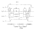
この場合、電源投入時の回路ブロックCT2内トランジスタの基板電圧は図2のように制御される。
【0024】
基板NW、PWの電圧VBP、VBNは最初に投入された3.3Vをもとに作られるが、この電圧は低い電源電圧で動作する回路ブロックCT2内のトランジスタを十分カットオフする値に選ばれる。例えば、PMOSFETに対しては3.3Vで、NMOSFETに対しては−1.5Vである。まず、この基板電圧を回路ブロックCT2に与え、その後で低い電源電圧Vcc2を与える。したがって、低い電源電圧を投入する過程では、回路ブロックCT2内トランジスタのしきい値電圧VTは十分大きいので各トランジスタからのサブスレッショルド電流が累積されて過大なチップ電流になることもないし、各トランジスタの基板電圧は0V程度のフローティング状態とはならないのでラッチアップを起こすことはない。
【0025】
その後、基板NW、PWの電圧VBP,VBNを浅くすることで(例えば、2.3Vと−0.5V程度)、回路ブロックCT2内のトランジスタのしきい値電圧VTを低くして通常動作に移行させ、主要回路の動作を開始させる。回路ブロック内のクロックを停止する(クロックをハイレベル又はローレベルに固定する)スタンバイ時、スリープ時あるいはチップの非選択時には基板電圧VBP、VBNを深く(例えば、3.3Vと−1.5V)することで回路ブロックCT2内のトランジスタのしきい値電圧VTを高くする。これによりサブスレッショルド電流による消費電力増加を減少させることができる。
【0026】
電源遮断時には基板電圧VBP、VBNを十分深くしてからVcc2をオフにし、その後に電源電圧Vcc1をオフにする。ここで電源電圧の印加順序は、例えば、高い電源電圧Vcc1が印加されてから、タイマーなどによって時間間隔を作り、その後、低い電源電圧Vcc2を入力すればよい。また回路ブロックCT1と回路ブロックCT2は異なる半導体チップで構成しても、あるいは同一チップ上に集積してもよい。
【0027】
図3は回路ブロックCT1と回路ブロックCT2を同一チップ上に集積した実施例である。I/Oはチップ外とのインターフェース回路、LG1からLG4は基板電圧を制御させる回路ブロックで、低しきい値電圧VTトランジスタを含む回路で構成されている。SRAMはスタティックメモリセルで構成されたメモリアレイSARYを含むスタティックメモリで、VCCSはメモリセルへの電力供給電源電圧である。DRAMは1個のMOSFETとキャパシタから成るダイナミックメモリセルで構成されたメモリアレイDARYを含むダイナミックメモリで、Vpはキャパシタ電極電圧である。DL、/DLはデータ線で、WLはワード線である。
【0028】
とくに限定しないが、メモリアレイSARYおよびメモリアレイDARYはここでは高しきい値VTトランジスタで構成されているものとする。VBは基板電圧発生回路で、基板電圧制御回路CLGからのコントロール信号群(φp、/φp、φ1、/φ1、φ2、/φ2、φ3、/φ3、φ4、/φ4)によって制御されている。VBAはメモリアレーへの基板電圧発生回路であり、メモリアレイSARYおよびメモリアレイDARY内の基板電圧VPS、VNS、VNDを供給している。これらの基板電圧VPS、VNS、VNDは通常は直流電圧あるいは準直流電圧である。ここで基板電圧発生回路VB、基板電圧制御回路CLGおよび基板電圧発生回路VBAからなる回路ブロックCT1の主要部は高しきい値電圧VT のMOSFETで構成されている。また、インターフェース回路I/Oおよび基板電圧発生回路VBには高い電源電圧(Vcc1)が供給され、その他の回路ブロックには低い電源電圧(Vcc2)が供給されている。
【0029】
ここでメモリアレイSARYおよびメモリアレイDARYは他の回路とは異なる性質を持っているので、基板電圧の与え方は異なっている。すなわち、メモリアレイ部はチップ全体に占める面積の割合が大きいので、一般に高密度が望ましい。このためには素子間分離幅を狭くしなければならない。これは一般にメモリアレイ全体に一定の実質的に直流である基板電圧を与える基板バイアス方式と併用されて実現されることが多い。もしこの部分の基板容量を駆動すると素子分離特性が劣化する以外に、この基板容量が大きいためにチップ全体の消費電力を増大するなどといった問題点が生じるためである。したがって、通常はメモリアレイSARY内の基板電圧VNSは0Vに、基板電圧VPSは電源電圧Vccsに等しく設定され、またメモリアレイDARYでは基板電圧VNDは−1.5V程度の実質的に直流である電圧が与えられる。ここでメモリアレイSARY内のメモリセルはフリップフロップなので、それを構成するトランジスタのしきい値電圧VTが小さすぎるとセル内のサブスレッショルド電流が増加する。メモリアレイSARYは多数のメモリセルで構成されるからメモリアレイSARY全体としてはこの電流は大きな値となる。そこでこれらセル内トランジスタのしきい値電圧VTは例えば0.5V程度と大きくし、その大きなしきい値電圧VTに見合うだけの高い電源電圧Vccsに設定するとセルは高速に動作する。例えば電源電圧Vccsは電源電圧Vcc2(1.8V)よりも大きな電源電圧Vcc1(3.3V)にするのも電源電圧の数を増やさないので有効である。
【0030】
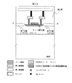
図4は、図3の代表的なデバイス断面構造の概略図である。スタティックメモリSRAMのメモリアレイ部ならびにダイナミックメモリDRAMのメモリアレイ部のキャパシターについては図面を分かり易くするために省略している。
【0031】
以下図3のチップを前提に、内部の各回路ブロックに上述した発明を具体的に適用した例を述べる。
【0032】
図5は図3の回路ブロック(LG1からLG4)内部のサブ回路ブロックに適用した本発明の一実施例である。回路ブロックCT2内の低しきい値電圧VT を有するMOSFETの基板(NW、PW)電圧は、回路ブロックCT1および回路ブロック/CT1によって制御されている。本実施例では、この制御をキャパシタ(CP,CN)を利用して行うことに特長がある。基板電圧発生・制御回路VBは、コントロール信号(φp,φ,/φp,/φ)と基板バイアス電圧(VBP,VBN)を高い電源電圧Vcc1(例えば3.3V)から発生し、出力するようにされる。pチャネルトランジスタ(PMOSFET)QPPおよびnチャネルトランジスタ(NMOSFET)QPNは高しきい値電圧VTを有するトランジスタである。
【0033】
図6に図5の回路の動作を示す。基板バイアス電圧VBP,VBNは一般には基板電圧発生・制御回路VBによって最初に投入された3.3Vをもとに作られるが、基板バイアス電圧VBPとして直接Vcc1(3.3V)で代用する例で説明する。まず、この基板バイアス電圧VBPを回路ブロックCT2に与え、その後で低い電源電圧Vcc2を与える。したがって、低い電源電圧Vcc2を投入する過程では、回路ブロックCT2内のトランジスタのしきい値電圧VTは例えば、0.5Vと十分大きく、pn接合は順方向にバイアスされることはないので、各トランジスタからのサブスレッショルド電流が累積されて過大なチップ電流になることはないし、ラッチアップを起こすこともない。通常動作に移行する際には、制御信号φpおよび/φpをそれぞれ高い電圧('H')、低い電圧('L')レベルにしトランジスタQPPおよびQPNをオフさせ,その後,制御信号φおよび/φをそれぞれ'L','H'レベルにする。かくてキャパシタ(CP,CN)結合で基板(NW,PW)電圧は変化し、それぞれ例えば2.3Vおよび-0.5V程度になる。基板の電圧が浅くなるので、回路ブロックCT2内のトランジスタのしきい値電圧VTが小さくなる。したがって、高速動作が可能となる。次にこの状態からスタンバイ、スリープあるいはチップの非選択モードに移行するには、制御信号φpおよび/φpを'L'および'H'にしてトランジスタQPPおよびQPNをオンさせ、その後、制御信号φおよび/φをそれぞれ'H','L'レベルに戻す。基板に深い電圧がかかるために回路ブロックCT2内のトランジスタのしきい値電圧VTが例えば、0.5Vと大きくなる。したがって、サブスレッショルド電流による消費電力増加をなくすことができる。
【0034】
このように動作モードに応じて基板電圧を変える動作は、コンデンサ(CP,CN)による容量結合で行われるので瞬時に行える利点がある。しかし、ソースやドレインのpn接合リーク電流あるいはMOSFETの基板電流によって基板電圧は徐々に浅くなる。特にこの基板電流は、動作周波数に比例して大きくなる。図6の基板(ウェル)リフレッシュはこれを2.3Vと -0.5Vに復帰させるための動作である。特に限定しないが、基板電圧をモニタしたり、あるいはタイマによって決められた時間でこのリフレッシュ動作を行う。このリフレッシュ動作は、通常動作状態にある回路を、一度スタンバイ状態にして再度通常動作状態に戻すという動作である。尚、チップを高速動作させる場合のリフレッシュ間隔を、低速動作させる場合のそれよりも短くするといったように、基板電流の大きさに応じてリフレッシュ間隔を可変にすることも動作の信頼性を向上させるのに有効である。
【0035】
図7は図5のトランジスタ(QPP,QPN)及びキャパシタ(CP,CN)のレイアウト例である。図8は図7のレイアウトの断面図(B---B’断面)である。図32は図7のレイアウトの断面図(C---C’断面)である。基板バイアス電圧VBP,VBNは第二配線層(第二金属配線層)でトランジスタQPP及びQPNのソースに接続される。トランジスタQPP及びQPNのドレインは第二配線層に接続され、主要回路に給電する基板電圧NWおよびPWを出力する。また、キャパシタCP,CNはMOS容量によって形成されている。
【0036】
図9は図5の応用例で、2個のサブ回路ブロックCT2(1),CT2(2)のいずれか一方を選択駆動する例である。ウエルブロック選択信号WBと起動クロックφによって選択サブ回路、例えば、サブ回路ブロックCT2(1)に属する基板電圧発生回路CT1(1),/CT1(1)のみが選択駆動され、それに属するウエルNW(1),PW(1)の電圧はCT2(1)内のMOSFETのしきい値電圧VTを低下させるように駆動される。一方非選択サブ回路ブロックCT2(2)のウエルは駆動されないのでサブ回路ブロックCT2(2)内のMOSFETのしきい値電圧VTは大きな値のままである。このように分割選択駆動しないと、サブ回路ブロックCT2(1)とサブ回路ブロックCT2(2)の全体のウエルを駆動する必要があるし、通常動作中に低しきい値電圧VTによって流れるサブスレッショルド電流はサブ回路ブロックCT2(1)とサブ回路ブロックCT2(2)内のすべてのMOSFETから流れる。したがって、本実施例ではパルス駆動に伴う電力もサブスレッショルド電流も半減することになる。
【0037】
図10は、図9の例をメモリ(DRAM,SRAM)の行デコーダとドライバに適用した例である。通常メモリアレーは多数のサブアレーに分割され、サブアレー対応に行デコーダとワード線駆動回路(ワードドライバ)が配置されている。しかし、実際に選択・駆動されるサブアレーは少数であることに着目すると、選択されるサブアレーに属する行デコーダとワードドライバ内のMOSFETのウエルはしきい値電圧VTが小さくなるように駆動し、他の大部分の非選択サブアレーのそれは駆動せずにしきい値電圧VTが大きなままに保持しておけば、全体としては消費電力もサブスレッショルド電流も激減する。
【0038】
図10では2個のサブアレーARY1,ARY2の例を概念的に示した。サブアレー ARY1,ARY2はそれぞれ128本のワード線(WL)と複数のデータ線DL(図中では簡単のため1本のみ示した)から成り、その交点にメモリセルMCが接続されている。それぞれのワード線(WL)にはCMOSインバータ(QDP,QDN)から成るワードドライバdrvとワード線を選択する行デコーダdecが接続されている。デコーダdecはNMOSFETが直列接続されたNAND論理で、それぞれのゲートには内部アドレス信号ai,...ajなどが入力されている。
【0039】
外部クロックCLKが’H’(3.3V)の状態ではプリチャージされている。その後クロックCLKが’L’(0V)になるとPMOSFET QPPはオフとなり、内部アドレス信号は外部アドレスAi,...Ajの論理状態に応じて0Vから1.8Vあるいは0Vとなる。例えば、ワード線WL1を選択するアドレス信号の場合には、ワード線WL1に接続されたデコーダdecのNMOSFETのすべてがオンとなり、ワードドライバdrvの入力は0Vに放電しPMOSFET QDPはオンする。この結果ワード線WL1には1.8Vのパルス電圧が出力される。ここで選択されたワード線WL1を含む回路ブロックCT2(1)内のウエルNW(1),PW(1)をしきい値電圧VTを小さくするように駆動しておけば、デコーダdecからワード線WL1にパルスが出力するまでの時間は高速化できる。また非選択回路ブロックCT2(2)内のウエルは駆動されることはないので、パルス駆動に伴う電力の増加やサブスレッショルド電流の増加はない。ウエルブロックセレクタは、内部アドレス信号によっていずれの回路ブロックのウエルを駆動するかを選択する。
【0040】
図11は図5の回路ブロックCT2を一個のインバータにし、さらに制御信号φおよび/φを入力信号INから生成した場合の実施例である。入力信号INが'L'から'H'に変化すると、基板(NW、PW)の電圧はそれぞれキャパシタ(CP,CN)によるカップリングで高くなる。したがって、PMOSFETのしきい値電圧VTは大きくなるのでサブスレッショルド電流が小さくなる。また、NMOSFETのしきい値電圧VTが低くなるのでインバータの負荷駆動力が増加する。逆に、入力信号INが'H'から'L'に変化すると、基板電圧は逆に低くなる。したがって、今度はPMOSFETのしきい値電圧VTは低くなり、負荷駆動力が増加し、また、NMOSFETのしきい値電圧VTが高くなるのでサブスレッショルド電流が小さくなる。このように入力信号によって自動的にMOSFETのしきい値電圧VTが変化し、サブスレッショルド電流を抑えながら、インバータの負荷駆動能力を増加させることができる。制御信号φpおよび/φpは電源投入時などあるいは前述したリフレッシュに用いる。基板は図5と同様、基板(ウェル)リフレッシュが必要である。以上の動作の詳しいタイミングチャートを図12に示す。VTPならびにVTNはそれぞれPMOSFETとNMOSFETのしきい値電圧VTで、ここでは区別して表現している。ウェル(NW,PW)の最高電圧と最低電圧は、トランジスタQPPとQPNがダイオードとして働くために、それぞれVBP+VTP, VBN−VTNにクランプされる。
【0041】
図13は図11の回路のレイアウト例である。図14は図11のレイアウトの断面図である。トランジスタQPP,QPNはウェルを分離して形成する必要があり、またキャパシタCP,CNは、基板を給電している表面高濃度層までゲート電極を延長することで実現している。
【0042】
図15は図11の回路と同様の機能を持つ他の実施例である。キャパシタCP,CNはインバータ列INVを介して接続されている。このインバータ列INVは、それらの消費電力を小さくするために高いきい値電圧VTのMOSFETで構成されていてもよいし,あるいは低いきい値電圧VTのMOSFETであるが、ゲート幅W/ゲート長Lの小さなMOSFETで構成されていてもよい。図11ではインバータの入力容量はキャパシタCP,CNによって大きくなるが、本実施例ではインバータがバッファになるのでそれを抑えることができる。図16は2個のインバータ列INVを一つにまとめた実施例で、入力容量と面積をさらに小さくすることができる。
【0043】
図17は図15の発明を複数のインバータ列に適用した実施例、すなわち、インバータIV1、IV2、IV3、IV4が直列に接続された回路の例である。トランジスタQPP,QPNとキャパシタCP,CNを複数のインバータで共用しているので実効的に小面積になる。すなわち、導通させるMOSFETのしきい値電圧VTを小さくし、非導通にさせるMOSFETのしきい値電圧VTは大きくさせるために、基板(ウェル)は1個毎に結線した2種のウェル配線が必要になるが、トランジスタQPP1,QPN1ならびにインバータ列INVとキャパシタCpはインバータIV2とIV4で、またトランジスタQPP2,QPN2ならびにインバータ列INVとキャパシタCNはインバータIV1とIV3で共用している。このような共用は図11及び図16の実施例にも適用できることは言うまでない。
【0044】
図18は図11の発明をNOR論理回路に応用した例である。図中(a)、(b)はそれぞれPMOSFET、NMOSFETで構成している。(a)では入力(I1,I2)の少なくても一方が’L’になるとそれまで’L’であった出力Outには’H’が出力される。(b)では入力の少なくても一方が’H’になるとそれまで’H’であった出力Outには’L’が出力される。
【0045】
図19は図11の発明をNAND論理回路へ応用した例である。出力Outは最初プリチャージ信号φPと低しきい値電圧VTのPMOSFETで1.8Vにプリチャージされ、入力(I1,I2)はすべて’L’(0V)である。その後入力のすべてが’H’(1.8V)になると直列接続されたNMOSFETはすべて導通し、フローティング’H’であった出力は0Vに放電する。この回路は図10の行デコーダにも応用できる。(b)はウエルのプリチャージMOSFETを共有し面積を減らした例である。ウエルの容量が(a)に比べて2倍になっても入力I1と入力I2に接続された2個のキャパシタでウエルを駆動する。したがって、ウエル電位の変化は(a)と同じとなって出力Outを高速に放電することができる。(c)はPMOSFETで構成したものである。入力I1,I2が同時に’L’になると、それまで0Vにプリチャージされていた出力Outは’H’に充電される。
【0046】
次に図3のインタフェース回路I/Oへの応用について述べる。図20はチップ外からの入力(In)バッファである。(a)は高い電流電圧3.3Vと高いきい値電圧VT のMOSFETを用いたよく知られた回路である。(b)はトランジスタQPとQNに小さなしきい値電圧VTのMOSFETを用いた例である。トランジスタQPPとQPNは大きなしきい値電圧VTでスイッチの役目をする。入力バッファが不必要な時間帯はトランジスタQPP,QPNをオフにして、電源電圧VCC1とアース間に流れるトランジスタQPとQNのサブスレッショルド電流を阻止する。有効な信号が入力される時間帯ではトランジスタQPP,QPNをオンにする。
【0047】
図21は、インタフェース回路I/Oのデータ出力段に図11の発明を適用したものである。汎用のダイナミックメモリ(DRAM)チップなどに多用されているように、CMOSラッチアップ等のノイズ耐性を向上するために、インタフェース回路I/O内のデータ出力段を同極性例えば、NMOSFETで構成し低電源電圧Vcc2で駆動した例である。出力(Dout)部は、同じ様な出力バッファ回路が複数個共通に接続されたWired OR(ワイアド・オア)回路になっている。Wired OR接続では、ある1個の出力回路が選択されて共通結線された出力Dout部にデータが出力されている期間中は、他の出力バッファ回路は完全にオフである必要がある。またすべての出力バッファ回路が非選択の場合には共通出力(Dout)部は完全にオフでなければならない。低電圧・低しきい値電圧VT動作のもとでこれを実現するには上述した発明が有効である。図ではトランジスタQN1およびQN2は低しきい値電圧VTの出力段NMOSFETで、それらの基板(ウェル)電圧を与えるトランジスタQPN1およびQPN2は高しきい値電圧VTのPMOSFETである。この回路の特長は、対となるデータ出力信号do,/doの情報に応じて出力段MOSFET(QN1,QN2)のしきい値電圧VTを変えることにある。まず、トランジスタQPN1,QPN2をオンすることで基板PW1およびPW2を基板バイアス電圧VBNの電位にプリチャージする。この電位ではトランジスタQN1,QN2QN間に流れるサブスレッショルド電流は無視できる値になるように設定しておく。その後、出力信号do、/doが情報に応じて’H’と’L’,あるいは’L’と’H’の組み合わせになることで出力Doutにデータが出力される。その際、導通する方のNMOSFETの基板電圧はキャパシタによるカップリングでそのしきい値電圧VTが低くなるので負荷駆動能力が向上し高速になる。駆動されない他方のNMOSFETのしきい値電圧VTは高いままなのでサブスレッショルド電流は無視できる。
【0048】
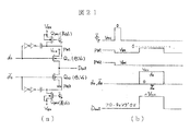
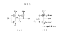
図22はウエル(NW)駆動回路の具体例である。(a)は図5の制御信号φをCMOSインバータから発生させる例である。ウエルの寄生容量とキャパシタCPの比を調整することによって、例えば、図6のウエルNWの電圧2.3Vを発生させることができる。(b)はキャパシタCPを使わずに、直接2.3V電源電圧をウエルNWに印加する回路である。制御信号φは0Vから3.3Vの電圧範囲をとり、トランジスタQNのソース電圧は2.3Vである。したがって、制御信号φが0VでトランジスタQNは低しきい値電圧VTでもトランジスタQNは十分にカットオフできる。また、制御信号φ3.3Vになると低しきい値電圧VTなので高速にウエルNWを駆動できる。ここで2.3Vは、外部電圧3.3Vをチップ内部で降圧させて作ることができる。
【0049】
図23は本発明の他の実施例である。VB1,VB2は電源電圧Vcc1からチップ内部で基板(ウェル)電圧を発生させる回路(後述)である。大きなしきい値電圧VTであるMOSFET(QPP, QPN)は、発生させた基板電圧を主要回路のMOSFETの基板に給電するときにオンするスイッチの役目をする。例えば、前述したようにスタンバイ時等である。キャパシタCBP,CBNは主要回路のMOSFETの基板容量である。キャパシタCPP,CPBは、キャパシタCBPおよびCBNよりも十分大きな値に選ばれるようにされるので、上記スイッチがオンしても基板電圧の変動は小さい。これらのキャパシタは他の回路と同一チップ上に形成してもよいし、チップ外で例えばタンタルコンデンサや電解コンデンサで形成してもよい。チップ外で形成する場合には図中のノードN1,N2がパッケージ端子となり、そこにキャパシタが外付けされるので端子数が増加する。しかし容易に大きな容量を得ることができる。 このためキャパシタCPP,CPBに予め蓄えられた大量の電荷のほんの一部をキャパシタCPB, CBNに移すだけでよいので、高速にスタンバイ状態に必要な基板電圧に設定できる。基板電圧発生回路VB1およびVB2の電源容量は一般に小さいので、それらを通してキャパシタCBPおよびCBNを充電するといった問題点はない。もちろん、基板電圧発生回路VB1,VB2は使わずに、ノードN1,N2にチップ外部からパッケージ端子を介して直接に所要基板電圧を印加することもできる。
【0050】
図24〜図26は、これまで使用を前提としてきた基板バイアス電圧VBN,基板バイアス電圧VBP,降圧電圧VCLを発生する電源回路の概念図である。詳細は単行本「超LSIメモリ」(伊藤清男著,培風館、1994年11月5日発行,239〜328頁)に記載されている。図24は3.3V電源をもとに負電圧(例えば、−1.5V)電源を作る例である。リングオシレータとダイオード接続のMOSFETから成る。図25は3.3V電源をもとに3.3V以上の昇圧電源を作る例である。チップ内のリングオシレータと昇圧キャパシタを用いる。尚、これまではVBP=3.3Vを仮定した説明が多かったが、この場合にはこのような昇圧電源はもちろん不要である。しかし基板バイアス電圧VBPなどの値はMOSFETの特性で決められるので、一般にはこのうようなVCC1(3.3V)以上の昇圧電源が必要である。図26は3.3V電源を用いて降圧電圧VCL(2.3V)を得る例である。降圧電圧VCLの値はチップ内で発生させた参照電圧VREFとコンパレータで決めることができる。
【0051】
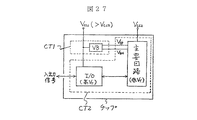
以上、図3の内部回路への適用例を中心に述べてきたが、本発明の適用はこれに限定されることはない。図27は図3に示した実施例をより簡単に図示したもので、これをもとに他の実施例を述べる。インタフェース回路I/Oはチップ外部とのインターフェースを行い、主に高しきい値電圧VTのMOSFETで構成されており、高い電源電圧Vcc1が印加されている。基板電圧発生回路VBには、高い電源電圧Vcc1(> Vcc2)が印加され、基板バイアス電圧VBPおよびVBNを発生するようにされる。主要回路は低しきい値電圧VTのMOSFETで構成され、低い電源電圧(Vcc2)が印加されている。当然ながら前述したように、I/Oは全てが高いVTのMOSFETで構成されていなくてもよいし、主要回路の全てが低しきい値電圧VTのMOSFETで構成されている必要はない。また、基板電圧発生回路VBの出力であるPMOSFETの基板バイアス電圧VBPは、主要回路内のPMOSFETのしきい値電圧VTを十分高い値(実際にはPMOSFETなのでしきい値電圧VTは絶対値)にできれば電源電圧Vcc1を直接基板バイアス電圧VBPとみなして使うこともできる。
【0052】
図28は図2で説明した本発明の電源投入に関する発明を単一電源のチップに適用した例である。基板バイアスモニタ回路DTは、電源投入時に基板電位が十分安定に供給できたことを検出する回路である。その検出出力によって高しきい値電圧VTのPMOSFETをオンさせ、インタフェース回路I/Oと主要回路に電源電圧Vccを供給している。
【0053】
図29は降圧電源回路VDを用いた実施例である。高い電源電圧Vccから低い電源電圧VcLを降圧電源回路VDによって生成し、主要回路に給電している。この場合、単一電源で、主要回路を構成するデバイスの最適動作電圧になるように降圧電圧VCL、基板バイアス電圧VBP,VBNを内部で調整できる利点がある。もちろんこの場合にも基板バイアス電圧VBPとVBNが印加されてから降圧電圧VCLを印加する。
【0054】
図30は外部電源が2種(VCC1,VCC2)の場合にでもユーザに電源投入順序に対する制約を与えない方式例である。低しきい値電圧VTを多用する主要回路には図28の発明を適用し低電圧(VCC2)電源で動作させる。一方、高しきい値電圧VTのMOSFETを多用するインタフェース回路I/Oは他の電源電圧(例えば、VCC1)で動作させ。インタフェース回路I/Oと主要回路間には動作電圧の差があるので小規模な電圧レベル変換回路が必要であるが、電源電圧VCC1で動作する回路ブロックと電源電圧VCC2で動作する回路ブロックはほぼ独立に動作し、低しきい値電圧VTの主要回路のラッチアップも防げるから、ユーザにとって使い易いチップが実現できる。
【0055】
図31はこの場合の内部回路の動作を示している。図5に対応した回路である。本例ではインタフェース回路I/Oは1.8Vの高電圧電源で動作し、主要回路は1.2Vの低電圧電源で動作するものとしている。電源電圧VCC2で動作する昇圧回路によって昇圧(VBP=2.7V)電源を作り、制御信号φPは0Vから基板バイアス電圧VBPまでのパルス振幅をとる。また、制御信号φ,/φは、例えば、0Vから基板バイアス電圧VBPまでのパルス振幅をとる。負電圧電源回路によってVBN(-1.5V)がつくられ、制御信号/φPは0Vから基板バイアス電圧VBPまでのパルス振幅をとる。したがって、電源電圧VCC2が電源投入時にトランジスタQPPとQPNがオンとなって低しきい値電圧VTのトランジスタQP,QNに十分なウエル電圧が与えられてから、図30のトランジスタQがオンになって図31の低しきい値電圧VTの主要回路に電源電圧VCC2(VCC2印加よりも遅れて印加されるのでVCC2と区別してある)が印加される。
【0056】
以上の実施例では、トランジスタの構造およびその基板構造は特に限定しない。SOI(Silicon(Semiconductor) on Insulator)構造のようなMOSFETを用いてもよい。要は基板電圧によってしきい値電圧VTが制御できるような構造のトランジスタであればよい。また大きな電源電圧(例えば、Vcc1)が印加されるMOSFETのゲート酸化膜を、小さな電源電圧(例えば、Vcc2)が印加されるMOSFETのそれよりも厚くすれば、チップ全体として高信頼性が保証されることは言うまでもない。また図3ではあらゆる機能ブロックをチップ内に集積した例を示したが、それぞれ独立したチップ、例えば、ダイナミックメモリ(DRAM)チップ、スタティックメモリ(SRAM)チップあるいはマイクロプロセッサチップにでも本発明を適用できる。
【0057】
【発明の効果】
本願において開示される発明のうち代表的なものによって得られる効果を簡単に説明すれば下記の通りである。
【0058】
すなわち、高速・低消費電力で動作の安定なCMOS回路、及びそれで構成されたCMOS LSIチップならびに半導体装置が実現できる。
【図面の簡単な説明】
【図1】本発明によるCMOS半導体装置を示す。
【図2】本発明によるCMOS半導体装置の動作タイミングを示す。
【図3】本発明によるCMOS LSIチップを示す。
【図4】本発明によるCMOS LSIチップの断面の概略をを示す。
【図5】本発明によるCMOS回路を示す。
【図6】本発明によるCMOS回路の動作タイミングを示す。
【図7】図5の回路のレイアウトを示す。
【図8】図5の回路のレイアウトの断面の概略を示す。
【図9】本発明による回路サブブロックの選択・駆動法を示す。
【図10】本発明による行選択回路とその動作タイミングを示す。
【図11】本発明によるCMOSインバータを示す。
【図12】本発明によるCMOSインバータの動作タイミングを示す。
【図13】図11の回路のレイアウトならびにその断面を示す。
【図14】図11の回路のレイアウトの断面を示す。
【図15】図11の回路の変形例を示す。
【図16】図11の回路の変形例を示す。
【図17】本発明をインバータ列に適用した例を示す。
【図18】本発明によるNOR論理回路を示す。
【図19】本発明によるNAND論理回路を示す。
【図20】入力バッファ回路の例を示す。
【図21】本発明によるデータ出力回路を示す。
【図22】本発明によるウエル駆動回路を示す。
【図23】本発明によるウエル電圧の印加方式をを示す。
【図24】負電圧電源回路の従来例を示す。
【図25】昇圧電源回路の従来例を示す。
【図26】降圧電源回路の従来例を示す。
【図27】本発明による2電源チップの構成を示す。
【図28】本発明による単一電源チップを示す。
【図29】本発明による単一電源チップを示す。
【図30】本発明による2電源チップの構成を示す。
【図31】本発明による2電源チップの内部回路を示す。
【図32】図5の回路のレイアウトの別の断面の概略を示す。
【符号の説明】
Φ,/Φ,ΦP,/ΦP…ウエル電圧制御信号、NW…PMOSFETのウエル,
PW…NMOSFETのウエル、VBP…PMOSFETのウエル用電源電圧、
VBN…NMOSFETのウエル用電源電圧。[0001]
BACKGROUND OF THE INVENTION
The present invention relates to a semiconductor device, and is a technique particularly suitable for a semiconductor device having both high speed and low power.
[0002]
[Prior art]
Low power technologies using substrate bias control include, for example, 1996 IEE International Solid State Circuit Digest of Technical Papers, pages 166 to 167 (1996 IEEE International Solid-State Circuit, Digest of Technical Papers (1996) pp.166-167).
[0003]
[Problems to be solved by the invention]
In recent years, with the low voltage operation of CMOS LSI (Complementary Metal Oxide Semiconductor Large Scale Integrated Circuit), there is an active movement to maintain high-speed operation by reducing the threshold voltage V T of the MOSFET (transistor) as the operating voltage decreases. It has become. However, the power supply voltage becomes 2V below, reducing the threshold voltage V T below 0.5V transistor can not be completely cut off accordingly, so-called sub-threshold leakage current increases. For this reason, the standby current of the LSI chip is increased, which is an obstacle when designing a system composed of a CMOS LSI chip on the premise of battery operation, for example. It is even said that the current during normal operation increases as the threshold voltage V T further decreases.
[0004]
To overcome this gap, during normal operation, the threshold voltage V T of all MOSFETs in the chip is reduced to operate at high speed, and the standby voltage V T is set to a sufficiently large value during standby. Methods for reducing current are well known. However, this method has the following three problems.
[0005]
(1) Conventionally, an excessive current flows due to latch-up or the like when the power is turned on, and wiring in the CMOS LSI chip is blown. Or the current capacity of the power supply is exceeded, and a normal power supply voltage cannot be applied. This is due to the fact that the substrate (well) and source of the MOSFET are connected to a layout that is not equipotential. For example, take a p-channel MOSFET (PMOSFET) that provides a positive voltage supply to its source. When a positive voltage supply (e.g., 1.8V) is applied to the source (p layer), the well (n well) is floating 0V until just before that, so the pn junction between the source and well is excessive in the forward direction. Biased to cause CMOS latch-up. In conventional CMOS LSI products of 2V or more, the MOSFET well and source are connected as close as possible so that the potential of the MOSFET well and source are as equal as possible. The junction is not forward biased. In addition, since the threshold voltage V T is always constant and the value is set to approximately 0.5 V or more, the subthreshold current does not become a problem. The same is true for n-channel MOSFETs (NMOSFETs), but not as serious as PMOSFETs. When the power supply voltage is applied to the drain, the NMOSFET substrate (p-well) is fixed at the ground potential of 0V floating and the source is also 0V until just before that, so the pn junction formed by the drain and well is in order. This is because the direction is not biased. However, the subthreshold current flows between the drain and source when the threshold voltage V T is 0.5 V or less. The literature described in the above prior art, which features the separation and control of the well and the source, does not describe such a power-on problem, and the CMOS LSI has a low threshold voltage V T. This is a new problem.
[0006]
(2) The switching time from the normal operation mode to the standby mode or the switching time from the standby mode to the normal operation mode is on the order of μs and is extremely long. For example, consider the case where the substrate voltage is generated inside the same chip. Since the substrate voltage is generated based on a so-called charge pumping circuit that pumps a capacitor in the chip, its output current is limited to a low level. On the other hand, since the substrate power supply terminals are commonly connected by the transistors in the chip, the total substrate capacitance is extremely large (100 pF or more). Therefore, at the time of mode switching as described above, a large load (substrate) capacity is driven by a substrate voltage generation circuit having a low current driving capability, and the response time becomes long.
[0007]
(3) Since the threshold voltage V T of a CMOS circuit or a transistor in a circuit block in which there is no change in input / output voltage (so-called inactive state) during a normal operation period is small, even a CMOS circuit has a subthreshold. Current flows everywhere, increasing the operating current of the entire chip.
[0008]
The present invention relates to a transistor substrate (or well) voltage control method for solving these problems.
[0009]
An object of the present invention is to prevent latch-up that occurs at the time of power-on or power-off of a CMOS circuit including a low threshold voltage MOSFET.
[0010]
Another object of the present invention is to reduce the subthreshold current during normal operation.
[0011]
Another object of the present invention is to achieve low power consumption and highly stable operation while maintaining high speed in a CMOS circuit operating at a low voltage of 2 V or less, and an LSI and a semiconductor device using the CMOS circuit.
[0012]
The above and other objects and novel features of the present invention will be apparent from the description of this specification and the accompanying drawings.
[0013]
[Means for Solving the Problems]
The following is a brief description of an outline of typical inventions disclosed in the present application.
[0014]
That is, the well voltage of the CMOS circuit is controlled during power-on, normal operation, and power-off.
[0015]
(1) The semiconductor device applies a power supply voltage to the CMOS circuit after applying a well voltage so that the MOSFET can be cut off to a well of the CMOS circuit formed of a MOSFET that cannot be substantially cut off during normal operation.
[0016]
(2) The semiconductor device includes the first and second power supply voltages, and the third power supply voltage generated by the circuit including the voltage conversion circuit operating at the first power supply voltage is substantially sufficient during normal operation. A second power supply voltage is applied to the CMOS circuit after being applied as a well voltage so that the MOSFET can be cut off to the well of the CMOS circuit composed of a MOSFET that cannot be cut off.
[0017]
(3) A semiconductor device includes a circuit for fixing a well potential of a CMOS circuit including a MOSFET that cannot be substantially cut off during normal operation, and capacitively coupling the well potential of the MOSFET according to a change in an input signal of the CMOS circuit. A circuit for changing is provided.
[0018]
(4) The semiconductor device includes a dynamic memory cell composed of one MOSFET and a capacitor, and a CMOS circuit. During normal operation, the well potential of the MOSFET constituting the CMOS circuit is changed in pulses. The substrate voltage of the dynamic memory cell is substantially a DC power supply voltage.
[0019]
(5) A semiconductor device includes a static memory cell that operates with a large voltage and includes a MOSFET with a large threshold voltage, and a CMOS circuit that operates with a small voltage and includes a MOSFET with a small threshold voltage. The well potential of the MOSFET in the circuit is changed in pulses.
[0020]
(6) The semiconductor device includes at least one CMOS circuit, a standby control circuit, and a voltage conversion circuit, and supplies a voltage generated by the voltage conversion circuit to the standby control circuit. Is used to change the well potential of the CMOS circuit depending on the operating state, and a capacitor having a capacity larger than the well capacity is connected to the output of the voltage conversion circuit.
[0021]
DETAILED DESCRIPTION OF THE INVENTION
FIG. 1 shows an embodiment of the present invention. In the circuit block CT1 that operates at a high power supply voltage Vcc1 (for example, 3.3 V), the threshold voltage V T during operation of the internal transistor can be selected to be sufficiently large, for example, 0.5 V. Sufficiently high the power supply (operating) voltage, bother, it is the high-speed operation is possible even without a threshold voltage V T low such as 0.1 V. Accordingly, since the subthreshold current is negligibly small even if the threshold voltage V T during normal operation and standby is not switched, the source and substrate of these transistors can be connected to give the same voltage. Here, VB is a substrate voltage generation / control circuit controlled by control signals ФP and Ф.
[0022]
On the other hand, in the circuit block CT2 that operates at a low power supply voltage Vcc2 (e.g., 1.8 V), the threshold voltage V T of the internal transistor is reduced to, for example, 0.1 V during normal operation, and is operated at high speed. The standby current must be reduced to 0.5V. The control of the threshold voltage V T is performed by controlling the substrate NW, PW transistor.
[0023]
In this case, the substrate voltage of the transistor in the circuit block CT2 when the power is turned on is controlled as shown in FIG.
[0024]
The voltages V BP and V BN of the substrates NW and PW are created based on the 3.3V that was initially applied, but this voltage is selected to cut off the transistors in the circuit block CT2 that operates at a low power supply voltage. It is. For example, 3.3V for PMOSFET and -1.5V for NMOSFET. First, this substrate voltage is applied to the circuit block CT2, and then a low power supply voltage Vcc2 is applied. Therefore, in the process of applying a low power supply voltage, the threshold voltage V T of the transistor in the circuit block CT2 is sufficiently large, so that the subthreshold current from each transistor is not accumulated, resulting in an excessive chip current. Since the substrate voltage is not in a floating state of about 0V, latch-up will not occur.
[0025]
After that, by reducing the voltages V BP and V BN of the substrates NW and PW (for example, about 2.3 V and -0.5 V), the threshold voltage V T of the transistors in the circuit block CT2 is lowered to achieve normal operation. Transition and start operation of main circuit. Stops the clock in the circuit block (fixes the clock to high or low level). During standby, sleep, or when the chip is not selected, the substrate voltages V BP and V BN are set deep (for example, 3.3 V and -1.5 V). As a result, the threshold voltage V T of the transistors in the circuit block CT2 is increased. As a result, an increase in power consumption due to the subthreshold current can be reduced.
[0026]
When the power is shut off, the substrate voltages V BP and V BN are made sufficiently deep,
[0027]
FIG. 3 shows an embodiment in which the circuit block CT1 and the circuit block CT2 are integrated on the same chip. I / O is an interface circuit between the outside of the chip, LG1 from LG4 is a circuit block for controlling the substrate voltage, and a circuit including a low threshold voltage V T transistors. SRAM is a static memory including a memory array SARY composed of static memory cells, and V CCS is a power supply voltage for the memory cells. DRAM is a dynamic memory including a memory array DARY composed of a dynamic memory cell composed of one MOSFET and a capacitor, and Vp is a capacitor electrode voltage. DL and / DL are data lines, and WL is a word line.
[0028]
Although not particularly limited, it is assumed here that the memory array SARY and the memory array DARY are composed of high threshold V T transistors. VB is a substrate voltage generation circuit and is controlled by control signal groups (φp, / φp, φ1, / φ1, φ2, / φ2, φ3, / φ3, φ4, / φ4) from the substrate voltage control circuit CLG. VBA is a substrate voltage generation circuit to the memory array, and supplies substrate voltages V PS , V NS , and V ND in the memory array SARY and the memory array DARY. These substrate voltages V PS , V NS , and V ND are usually DC voltages or quasi-DC voltages. Here the substrate voltage generating circuit VB, the main portion of the circuit block CT1 consisting substrate voltage control circuit CLG and a substrate voltage generating circuit VBA is composed of a MOSFET of a high threshold voltage V T. Further, a high power supply voltage (Vcc1) is supplied to the interface circuit I / O and the substrate voltage generation circuit VB, and a low power supply voltage (Vcc2) is supplied to the other circuit blocks.
[0029]
Here, since the memory array SARY and the memory array DARY have different properties from other circuits, the method of applying the substrate voltage is different. That is, since the memory array portion has a large area ratio in the entire chip, a high density is generally desirable. For this purpose, the isolation width between elements must be narrowed. In general, this is often realized in combination with a substrate bias system that applies a constant substantially DC substrate voltage to the entire memory array. This is because, if the substrate capacitance of this portion is driven, the element isolation characteristic is deteriorated. In addition, since the substrate capacitance is large, problems such as an increase in power consumption of the entire chip occur. Therefore, normally, the substrate voltage V NS in the memory array SARY is set to 0 V, the substrate voltage V PS is set equal to the power supply voltage Vccs, and in the memory array DARY, the substrate voltage V ND is substantially a direct current of about −1.5 V. A certain voltage is given. Here, since the memory cells in the memory array SARY are flip-flops, the subthreshold current in the cells increases if the threshold voltage V T of the transistors constituting the memory cells is too small. Since the memory array SARY is composed of a large number of memory cells, this current has a large value for the entire memory array SARY. Therefore, the threshold voltage V T of these in-cell transistors is increased to, for example, about 0.5 V, and the cell operates at a high speed when the power supply voltage Vccs is set high enough to meet the large threshold voltage V T. For example, it is effective to set the power supply voltage Vccs to a power supply voltage Vcc1 (3.3V) larger than the power supply voltage Vcc2 (1.8V) because the number of power supply voltages is not increased.
[0030]
FIG. 4 is a schematic view of the typical device cross-sectional structure of FIG. The capacitors of the memory array portion of the static memory SRAM and the memory array portion of the dynamic memory DRAM are omitted for easy understanding of the drawing.
[0031]
An example in which the above-described invention is specifically applied to each internal circuit block will be described below based on the chip of FIG.
[0032]
FIG. 5 shows an embodiment of the present invention applied to sub-circuit blocks in the circuit blocks (LG1 to LG4) of FIG. The substrate (NW, PW) voltage of the MOSFET having the low threshold voltage V T in the circuit block CT2 is controlled by the circuit block CT1 and the circuit block / CT1. This embodiment is characterized in that this control is performed using capacitors (C P , C N ). The substrate voltage generation / control circuit VB generates and outputs a control signal (φp, φ, / φp, / φ) and a substrate bias voltage (V BP , V BN ) from a high power supply voltage Vcc1 (eg, 3.3 V). To be. The p-channel transistor (PMOSFET) Q PP and the n-channel transistor (NMOSFET) Q PN are transistors having a high threshold voltage V T.
[0033]
FIG. 6 shows the operation of the circuit of FIG. Substrate bias voltages V BP and V BN are generally generated based on 3.3 V initially applied by the substrate voltage generation / control circuit VB, but an example of directly substituting Vcc 1 (3.3 V) as the substrate bias voltage V BP I will explain it. First, given a substrate bias voltage V BP to the circuit block CT2, giving then a low power supply voltage Vcc2. Therefore, in the process of applying the low power supply voltage Vcc2, the threshold voltage V T of the transistor in the circuit block CT2 is sufficiently large, for example, 0.5 V, and the pn junction is not forward-biased. The sub-threshold current from is not accumulated, resulting in an excessive chip current, and no latch-up occurs. When shifting to normal operation, the control signals φp and / φp are set to the high voltage ('H') and low voltage ('L') levels, respectively, and the transistors QPP and QPN are turned off. Set / φ to 'L' and 'H' level, respectively. Thus, the substrate (NW, PW) voltage changes due to the capacitor (C P , C N ) coupling, and becomes, for example, about 2.3 V and −0.5 V, respectively. Since the substrate voltage becomes shallow, the threshold voltage V T of the transistors in the circuit block CT2 becomes small. Therefore, high speed operation is possible. Then stand in this state, the process proceeds to the non-selected mode of sleep or chip, control signals .phi.p and / φp 'L' and in the 'H' to turn on the transistors Q PP and Q PN, then, the control signal Return φ and / φ to the 'H' and 'L' levels, respectively. Since a deep voltage is applied to the substrate, the threshold voltage V T of the transistors in the circuit block CT2 increases to, for example, 0.5V. Therefore, an increase in power consumption due to the subthreshold current can be eliminated.
[0034]
Since the operation of changing the substrate voltage in accordance with the operation mode is performed by capacitive coupling using capacitors (C P , C N ), there is an advantage that it can be instantaneously performed. However, the substrate voltage gradually becomes shallow due to the source and drain pn junction leakage current or the MOSFET substrate current. In particular, this substrate current increases in proportion to the operating frequency. The substrate (well) refresh in FIG. 6 is an operation for returning this to 2.3V and -0.5V. Although not particularly limited, this refresh operation is performed at a time determined by monitoring the substrate voltage or by a timer. This refresh operation is an operation in which a circuit in a normal operation state is once set in a standby state and returned to a normal operation state again. It is also possible to improve the operation reliability by making the refresh interval variable according to the magnitude of the substrate current so that the refresh interval when operating the chip at high speed is shorter than that when operating at low speed. It is effective.
[0035]
FIG. 7 is a layout example of the transistors (Q PP , Q PN) and capacitors (C P , C N) of FIG. FIG. 8 is a sectional view (B --- B ′ section) of the layout of FIG. 32 is a sectional view (C --- C 'section) of the layout of FIG. The substrate bias voltages V BP and V BN are connected to the sources of the transistors Q PP and Q PN in the second wiring layer (second metal wiring layer). The drains of the transistors Q PP and Q PN are connected to the second wiring layer, and output substrate voltages NW and PW for supplying power to the main circuit. The capacitors C P and C N are formed by MOS capacitors.
[0036]
FIG. 9 is an application example of FIG. 5 and shows an example in which either one of the two sub circuit blocks CT2 (1) and CT2 (2) is selectively driven. Only the substrate voltage generation circuits CT1 (1), / CT1 (1) belonging to the selected subcircuit, for example, the subcircuit block CT2 (1) are selectively driven by the well block selection signal WB and the activation clock φ, and the well NW ( 1), the voltage of the PW (1) is driven so as to lower the threshold voltage V T of the MOSFET in the CT2 (1). On the other hand, since the well of the non-selected sub circuit block CT2 (2) is not driven, the threshold voltage V T of the MOSFET in the sub circuit block CT2 (2) remains a large value. If divisional selection driving is not performed in this way, it is necessary to drive the entire wells of the sub circuit block CT2 (1) and the sub circuit block CT2 (2), and the sub-flow that flows by the low threshold voltage V T during normal operation. The threshold current flows from all the MOSFETs in the sub circuit block CT2 (1) and the sub circuit block CT2 (2). Therefore, in this embodiment, both the electric power accompanying the pulse driving and the subthreshold current are halved.
[0037]
FIG. 10 is an example in which the example of FIG. 9 is applied to a row decoder and a driver of a memory (DRAM, SRAM). The normal memory array is divided into a number of subarrays, and a row decoder and a word line driving circuit (word driver) are arranged corresponding to the subarrays. However, paying attention to the fact that only a small number of subarrays are actually selected and driven, the row decoder belonging to the selected subarray and the well of the MOSFET in the word driver are driven so that the threshold voltage V T is reduced, If the threshold voltage V T is kept large without driving it in most other non-selected subarrays, overall power consumption and subthreshold current are drastically reduced.
[0038]
FIG. 10 conceptually shows an example of two subarrays ARY1 and ARY2. The subarrays ARY1 and ARY2 are each composed of 128 word lines (WL) and a plurality of data lines DL (only one is shown in the figure for simplicity), and a memory cell MC is connected to the intersection. Each word line (WL) is connected to a word driver drv comprising a CMOS inverter (Q DP , Q DN ) and a row decoder dec for selecting the word line. The decoder dec is NAND logic in which NMOSFETs are connected in series, and internal address signals ai,.
[0039]
When the external clock CLK is 'H' (3.3V), it is precharged. Thereafter, when the clock CLK becomes 'L' (0V) PMOSFET Q PP is turned off and the internal address signal becomes 1.8V or 0V from 0V depending on the logic state of the external address Ai, ... Aj. For example, in the case of the address signal for the word line WL 1 is selected, all the NMOSFET decoder dec connected to the word line WL 1 is turned on, the input of the word driver drv is turned on PMOSFET Q DP discharged to 0V . This is the result word lines WL 1 pulse voltage of 1.8V is output. Here the selected circuit block CT2 (1) including word lines WL 1 in the wells NW (1), if driven PW the (1) to reduce the threshold voltage V T, the decoder dec time of the word line WL 1 until the pulse outputs may speed. Further, since the wells in the non-selection circuit block CT2 (2) are not driven, there is no increase in power or subthreshold current due to pulse driving. The well block selector selects which circuit block of the well is driven by the internal address signal.
[0040]
Figure 11 shows an embodiment in which the circuit block CT2 of FIG. 5 in the one of the inverters, and further generates the control signals phi and / phi from the input signal I N. When the input signal I N changes from 'L' to 'H', the voltages of the substrates (NW, PW) become higher due to the coupling by the capacitors (C P , C N ), respectively. Therefore, the threshold voltage V T of the PMOSFET increases, so that the subthreshold current decreases. Further, since the threshold voltage V T of the NMOSFET is lowered, the load driving force of the inverter is increased. Conversely, if changes to the 'L' from the input signal I N is 'H', the substrate voltage is lowered to the contrary. Therefore, this time, the threshold voltage V T of the PMOSFET is lowered, the load driving force is increased, and the threshold voltage V T of the NMOSFET is increased, so that the subthreshold current is reduced. Thus automatic threshold voltage V T of the MOSFET changes depending on the input signal, while suppressing the subthreshold current can be increased to inverter load driving capability. The control signals φp and / φp are used when the power is turned on or for the refresh described above. As in FIG. 5, the substrate needs to be refreshed (well). A detailed timing chart of the above operation is shown in FIG. V TP and V TN are threshold voltages V T of PMOSFET and NMOSFET, respectively, and are expressed separately here. The highest and lowest voltages of the wells (NW, PW) are clamped to V BP + V TP and V BN −V TN , respectively, because the transistors Q PP and Q PN act as diodes.
[0041]
FIG. 13 is a layout example of the circuit of FIG. FIG. 14 is a cross-sectional view of the layout of FIG. The transistors Q PP and Q PN need to be formed separately from the wells, and the capacitors C P and C N are realized by extending the gate electrode to the surface high concentration layer feeding the substrate.
[0042]
FIG. 15 shows another embodiment having the same function as the circuit of FIG. Capacitors C P and C N are connected via an inverter array INV. This inverter array INV may be composed of a MOSFET having a high threshold voltage V T in order to reduce the power consumption thereof, or a MOSFET having a low threshold voltage V T , but has a gate width W / gate. It may be composed of a small MOSFET having a long length L. In FIG. 11, the input capacity of the inverter is increased by the capacitors C P and C N , but in the present embodiment, the inverter becomes a buffer, which can be suppressed. FIG. 16 shows an embodiment in which two inverter arrays INV are combined into one, and the input capacitance and area can be further reduced.
[0043]
FIG. 17 shows an embodiment in which the invention of FIG. 15 is applied to a plurality of inverter rows, that is, an example of a circuit in which inverters IV1, IV2, IV3, and IV4 are connected in series. Since the transistors Q PP and Q PN and the capacitors C P and C N are shared by a plurality of inverters, the area is effectively reduced. In other words, in order to reduce the threshold voltage V T of the MOSFET to be turned on and increase the threshold voltage V T of the MOSFET to be turned off, two types of well wirings in which the substrates (wells) are connected one by one Although is required, the transistor Q PP1, Q PN1 and inverter train INV and capacitor Cp by the inverter IV2 and IV4, also transistor Q PP2, Q PN2 and inverter train INV and the capacitor C N is shared by the inverters IV1 and IV3 Yes. It goes without saying that such sharing is also applicable to the embodiments of FIGS.
[0044]
FIG. 18 shows an example in which the invention of FIG. 11 is applied to a NOR logic circuit. In the figure, (a) and (b) are composed of PMOSFET and NMOSFET, respectively. In (a), when at least one of the inputs (I 1 , I 2 ) becomes “L”, “H” is output to the output Out that was previously “L”. In (b), when at least one of the inputs becomes 'H', 'L' is output to the output Out that was 'H' until then.
[0045]
FIG. 19 shows an example in which the invention of FIG. 11 is applied to a NAND logic circuit. Output Out is precharged to 1.8V at PMOSFET first precharge signal phi P and the low threshold voltage V T, the input (I 1, I 2) are all 'L' (0V). After that, when all the inputs become “H” (1.8V), all the NMOSFETs connected in series are turned on, and the output that was floating “H” is discharged to 0V. This circuit can also be applied to the row decoder of FIG. (b) is an example in which the well precharge MOSFET is shared to reduce the area. Even if the capacitance of the well is doubled compared to (a), the well is driven by two capacitors connected to the input I 1 and the input I 2 . Therefore, the change in well potential is the same as in (a), and the output Out can be discharged at high speed. (c) is composed of PMOSFET. When the inputs I 1 and I 2 simultaneously become “L”, the output Out that has been precharged to 0 V until then is charged to “H”.
[0046]
Next, application to the interface circuit I / O of FIG. 3 will be described. FIG. 20 shows an input (In) buffer from outside the chip. (a) is a well-known circuit using the MOSFET of the high current voltage of 3.3V and a high threshold voltage V T. (b) shows an example using a MOSFET of the small threshold voltage V T to the transistor Q P and Q N. Transistors Q PP and Q PN act as switches with a large threshold voltage V T. During the time period when the input buffer is not required, the transistors Q PP and Q PN are turned off to prevent the subthreshold currents of the transistors Q P and Q N flowing between the power supply voltage V CC1 and the ground. The transistors Q PP and Q PN are turned on during a time period when a valid signal is input.
[0047]
FIG. 21 shows the application of the invention of FIG. 11 to the data output stage of the interface circuit I / O. As commonly used in general-purpose dynamic memory (DRAM) chips, the data output stage in the interface circuit I / O is configured with the same polarity, for example, NMOSFET to improve noise immunity such as CMOS latchup. This is an example of driving with the power supply voltage Vcc2. The output (Dout) section is a Wired OR (wired OR) circuit in which a plurality of similar output buffer circuits are connected in common. In the Wired OR connection, the other output buffer circuit needs to be completely off during the period when one output circuit is selected and data is output to the commonly connected output Dout unit. When all output buffer circuits are not selected, the common output (Dout) section must be completely off. The above-described invention is effective for realizing this under the low voltage / low threshold voltage VT operation. In the figure, transistors Q N1 and Q N2 are output stage NMOSFETs having a low threshold voltage V T , and transistors Q PN1 and Q PN2 providing their substrate (well) voltages are PMOSFETs having a high threshold voltage V T. The feature of this circuit is that the threshold voltage V T of the output stage MOSFETs (Q N1 , Q N2 ) is changed according to the information of the paired data output signals do, / do. First, to precharge the substrate PW1 and PW2 to the potential of the substrate bias voltage V BN by turning on the transistor Q PN1, Q PN2. At this potential, the subthreshold current flowing between the transistors Q N1 and Q N2 Q N is set to a negligible value. Thereafter, the output signals do and / do become a combination of “H” and “L” or “L” and “H” according to the information, so that data is output to the output Dout. At that time, the substrate voltage of the conductive NMOSFET is reduced by the coupling by the capacitor, and the threshold voltage V T is lowered, so that the load driving capability is improved and the speed is increased. Since the threshold voltage V T of the other NMOSFET that is not driven remains high, the subthreshold current can be ignored.
[0048]
FIG. 22 shows a specific example of a well (NW) drive circuit. FIG. 5A shows an example in which the control signal φ in FIG. 5 is generated from a CMOS inverter. By adjusting the parasitic capacitance and the ratio of the capacitor C P well, for example, it is possible to generate a voltage 2.3V of well NW in Fig. (b) is without a capacitor C P, a circuit for applying a direct 2.3V power supply voltage to the well NW. Control signal φ takes the voltage range of 3.3V from 0V, the source voltage of the transistor Q N is 2.3V. Therefore, the transistor Q N can be sufficiently cut off even when the control signal φ is 0 V and the transistor Q N is at the low threshold voltage V T. Further, when the control signal becomes φ3.3V, the well NW can be driven at high speed because of the low threshold voltage V T. Here, 2.3V can be generated by stepping down the external voltage 3.3V inside the chip.
[0049]
FIG. 23 shows another embodiment of the present invention. VB1 and VB2 are circuits (described later) for generating a substrate (well) voltage from the power supply voltage Vcc1 inside the chip. MOSFETs (Q PP , Q PN ) having a large threshold voltage V T serve as a switch that turns on when the generated substrate voltage is supplied to the substrate of the MOSFET of the main circuit. For example, as described above, it is during standby. Capacitors C BP and C BN are the substrate capacities of the main circuit MOSFETs. Capacitors C PP and C PB are selected to be sufficiently larger than capacitors C BP and C BN, so that the substrate voltage variation is small even when the switch is turned on. These capacitors may be formed on the same chip as other circuits, or may be formed outside the chip by, for example, a tantalum capacitor or an electrolytic capacitor. In the case of forming outside the chip, nodes N1 and N2 in the figure serve as package terminals, and capacitors are externally attached there, so that the number of terminals increases. However, a large capacity can be easily obtained. For this reason, since only a small part of the large amount of charge stored in advance in the capacitors C PP and C PB has to be transferred to the capacitors C PB and C BN , the substrate voltage required for the standby state can be set at high speed. Since the power supply capacity of the substrate voltage generating circuit VB1 and VB2 are generally small, there is no problem that they through charging the capacitor C BP and C BN. Of course, the required substrate voltage can be directly applied to the nodes N1 and N2 from the outside of the chip via the package terminals without using the substrate voltage generating circuits VB1 and VB2.
[0050]
24 to 26 are conceptual diagrams of power supply circuits that generate the substrate bias voltage V BN , the substrate bias voltage V BP , and the step-down voltage V CL that have been assumed to be used so far. Details are described in the book “VLSI LSI” (written by Kiyoo Ito, Baifukan, November 5, 1994, pp. 239-328). FIG. 24 shows an example in which a negative voltage (for example, -1.5 V) power source is created based on a 3.3 V power source. It consists of a ring oscillator and diode-connected MOSFET. FIG. 25 shows an example of making a boost power supply of 3.3V or higher based on a 3.3V power supply. A ring oscillator and a boost capacitor in the chip are used. Until now, there have been many explanations assuming V BP = 3.3V, but in this case, such a boost power supply is of course unnecessary. However, since values such as the substrate bias voltage VBP are determined by the characteristics of the MOSFET, generally, such a boost power supply of V CC1 (3.3 V) or more is required. FIG. 26 shows an example in which the step-down voltage V CL (2.3 V) is obtained using a 3.3 V power source. The value of the step-down voltage VCL can be determined by a reference voltage VREF generated in the chip and a comparator.
[0051]
As described above, the application example to the internal circuit of FIG. 3 has been mainly described, but the application of the present invention is not limited to this. FIG. 27 illustrates the embodiment shown in FIG. 3 more simply, and another embodiment will be described based on this. Interface circuit I / O performs an interface with the outside of the chip, which is composed of a MOSFET mainly high threshold voltage V T, a high supply voltage Vcc1 is applied. A high power supply voltage Vcc1 (> Vcc2) is applied to the substrate voltage generating circuit VB to generate substrate bias voltages VBP and VBN . Main circuits are constituted by MOSFET with a low threshold voltage V T, low supply voltage (Vcc2) is applied. Of course, as mentioned above, not all I / Os need to be composed of MOSFETs with high V T , and all of the main circuits need not be composed of MOSFETs with low threshold voltage V T. . The substrate bias voltage V BP of the PMOSFET, which is the output of the substrate voltage generation circuit VB, is a sufficiently high value of the threshold voltage V T of the PMOSFET in the main circuit (actually the threshold voltage V T is absolute because it is a PMOSFET) it is also possible to use a power supply voltage Vcc1 if the value) directly regarded as the substrate bias voltage V BP.
[0052]
FIG. 28 shows an example in which the invention relating to power-on of the present invention described in FIG. 2 is applied to a single power source chip. The substrate bias monitor circuit DT is a circuit that detects that the substrate potential has been supplied sufficiently stably when the power is turned on. The detection output turns on the PMOSFET having the high threshold voltage V T and supplies the power supply voltage Vcc to the interface circuit I / O and the main circuit.
[0053]
FIG. 29 shows an embodiment using a step-down power supply circuit VD. The low supply voltage Vc L from a high power supply voltage Vcc generated by the step-down power supply circuit VD, and supplies power to the main circuit. In this case, there is an advantage that the step-down voltage V CL and the substrate bias voltages V BP , V BN can be adjusted internally so that the optimum operating voltage of the device constituting the main circuit can be obtained with a single power source. Of course, also in this case, the step-down voltage VCL is applied after the substrate bias voltages VBP and VBN are applied.
[0054]
FIG. 30 shows an example of a method in which the user is not restricted in the power-on sequence even when there are two types of external power sources (V CC1 and V CC2 ). The main circuit of FIG. 28 is applied to a main circuit that frequently uses the low threshold voltage V T and is operated with a low voltage (V CC2 ) power source. On the other hand, the interface circuit I / O that makes heavy use of MOSFETs with a high threshold voltage V T is operated with other power supply voltages (eg, V CC1 ). Since there is a difference in operating voltage between the interface circuit I / O and the main circuit, a small voltage level conversion circuit is required, but a circuit block that operates with the power supply voltage V CC1 and a circuit block that operates with the power supply voltage V CC2 Operates almost independently and prevents latch-up of the main circuit with a low threshold voltage V T , so that a user-friendly chip can be realized.
[0055]
FIG. 31 shows the operation of the internal circuit in this case. 6 is a circuit corresponding to FIG. In this example, the interface circuit I / O operates with a 1.8V high voltage power supply, and the main circuit operates with a 1.2V low voltage power supply. A booster (V BP = 2.7V) power supply is created by a booster circuit operating at the power supply voltage V CC2 , and the control signal φ P takes a pulse amplitude from 0 V to the substrate bias voltage V BP . Further, the control signal phi, / phi, for example, take the pulse amplitude of from 0V to the substrate bias voltage V BP. V BN (−1.5 V) is generated by the negative voltage power supply circuit, and the control signal / φ P takes a pulse amplitude from 0 V to the substrate bias voltage V BP . Therefore, when the power supply voltage V CC2 is turned on, the transistors Q PP and Q PN are turned on to give a sufficient well voltage to the transistors Q P and Q N having the low threshold voltage V T before the transistor shown in FIG. Q is (since it is applied later than V CC2 applied are distinguished from V CC2) supply voltage V CC2 to the main circuit of the low threshold voltage V T of Figure 31 turned on is applied.
[0056]
In the above embodiments, the transistor structure and the substrate structure are not particularly limited. A MOSFET having a SOI (Silicon (Semiconductor) on Insulator) structure may be used. In short it may be a transistor having a structure capable of controlling the threshold voltage V T by the substrate voltage. If the gate oxide film of a MOSFET to which a large power supply voltage (for example, Vcc1) is applied is thicker than that of a MOSFET to which a small power supply voltage (for example, Vcc2) is applied, high reliability is guaranteed for the entire chip. Needless to say. FIG. 3 shows an example in which all functional blocks are integrated in the chip, but the present invention can be applied to independent chips such as a dynamic memory (DRAM) chip, a static memory (SRAM) chip, or a microprocessor chip. .
[0057]
【The invention's effect】
The effects obtained by the representative ones of the inventions disclosed in the present application will be briefly described as follows.
[0058]
That is, it is possible to realize a CMOS circuit that is stable at high speed and with low power consumption, and a CMOS LSI chip and a semiconductor device including the CMOS circuit.
[Brief description of the drawings]
FIG. 1 shows a CMOS semiconductor device according to the present invention.
FIG. 2 shows an operation timing of the CMOS semiconductor device according to the present invention.
FIG. 3 shows a CMOS LSI chip according to the present invention.
FIG. 4 shows a schematic cross section of a CMOS LSI chip according to the present invention.
FIG. 5 shows a CMOS circuit according to the present invention.
FIG. 6 shows the operation timing of the CMOS circuit according to the present invention.
7 shows a layout of the circuit of FIG.
8 shows a schematic cross section of the layout of the circuit of FIG.
FIG. 9 shows a method for selecting and driving circuit sub-blocks according to the present invention.
FIG. 10 shows a row selection circuit according to the present invention and its operation timing.
FIG. 11 shows a CMOS inverter according to the present invention.
FIG. 12 shows the operation timing of the CMOS inverter according to the present invention.
13 shows a layout of the circuit of FIG. 11 and a cross section thereof.
14 shows a cross section of the layout of the circuit of FIG.
15 shows a modification of the circuit of FIG.
FIG. 16 shows a modification of the circuit of FIG.
FIG. 17 shows an example in which the present invention is applied to an inverter array.
FIG. 18 illustrates a NOR logic circuit according to the present invention.
FIG. 19 shows a NAND logic circuit according to the present invention.
FIG. 20 shows an example of an input buffer circuit.
FIG. 21 shows a data output circuit according to the present invention.
FIG. 22 shows a well drive circuit according to the present invention.
FIG. 23 shows a well voltage application method according to the present invention.
FIG. 24 shows a conventional example of a negative voltage power supply circuit.
FIG. 25 shows a conventional example of a boost power supply circuit.
FIG. 26 shows a conventional example of a step-down power supply circuit.
FIG. 27 shows a configuration of a dual power supply chip according to the present invention.
FIG. 28 shows a single power supply chip according to the present invention.
FIG. 29 shows a single power supply chip according to the present invention.
FIG. 30 shows a configuration of a dual power supply chip according to the present invention.
FIG. 31 shows an internal circuit of a dual power supply chip according to the present invention.
32 shows another cross-sectional schematic of the layout of the circuit of FIG.
[Explanation of symbols]
Φ, / Φ, Φ P , / Φ P … well voltage control signal, NW… well of PMOSFET,
PW… NMOSFET well, V BP … PMOSFET well supply voltage,
V BN … NMOSFET power supply voltage.
Claims (8)
上記CMOS回路は第1動作状態と第2動作状態とを有し、上記MOSFETに印加されるウェル電圧は上記第1動作状態において上記第2動作状態におけるよりも浅く制御されることで、上記第1動作状態における上記MOSFETのしきい値電圧の絶対値は上記第2動作状態における上記MOSFETのしきい値電圧の絶対値が小さくなるよう制御され、
電源投入過程において、上記MOSFETに所定のウェル電位を印加することにより上記MOSFETのソース・ウェル間のpn接合が順方向にバイアスされることによるCMOSラッチアップを防止した後に、上記CMOS回路の電源電圧を印加することを特徴とする半導体装置。In a semiconductor device having a CMOS circuit,
The CMOS circuit has a first operation state and a second operation state, and a well voltage applied to the MOSFET is controlled to be shallower in the first operation state than in the second operation state. The absolute value of the threshold voltage of the MOSFET in one operating state is controlled so that the absolute value of the threshold voltage of the MOSFET in the second operating state is small,
In the power-on process, a predetermined well potential is applied to the MOSFET to prevent CMOS latch-up due to forward bias of the pn junction between the source and well of the MOSFET, and then the power supply voltage of the CMOS circuit Is applied to the semiconductor device.
上記MOSFETはサブスレッショルド電流により、上記第1動作状態において実質的に十分カットオフできないMOSFETであることを特徴とする半導体装置。In claim 1,
The semiconductor device according to claim 1, wherein the MOSFET is a MOSFET that cannot substantially be cut off in the first operating state due to a subthreshold current.
上記ウェル電圧を制御するウェル電圧制御回路を有し、
電源遮断過程において、上記CMOS回路の電源電圧を遮断した後に、上記ウェル電圧制御回路の電源電圧を遮断することを特徴とする半導体装置。In claim 1 or 2,
A well voltage control circuit for controlling the well voltage;
A semiconductor device, wherein the power supply voltage of the well voltage control circuit is cut off after the power supply voltage of the CMOS circuit is cut off in the power cut-off process.
上記CMOS回路は第1動作状態と第2動作状態とを有し、上記MOSFETに印加されるウェル電圧は上記第1動作状態において上記第2動作状態におけるよりも浅く制御されることで、上記第1動作状態における上記MOSFETのしきい値電圧の絶対値は上記第2動作状態における上記MOSFETのしきい値電圧の絶対値が小さくなるよう制御され、
電源投入過程において、上記ウェル電圧制御回路により上記MOSFETのウェル電位を駆動した後に、上記CMOS回路の電源電圧を印加することを特徴とする半導体装置。A well voltage control circuit and a CMOS circuit;
The CMOS circuit has a first operation state and a second operation state, and a well voltage applied to the MOSFET is controlled to be shallower in the first operation state than in the second operation state. The absolute value of the threshold voltage of the MOSFET in one operating state is controlled so that the absolute value of the threshold voltage of the MOSFET in the second operating state is small,
In a power-on process, a semiconductor device is characterized in that after the well potential of the MOSFET is driven by the well voltage control circuit, the power supply voltage of the CMOS circuit is applied.
上記ウェル電圧制御回路の電源電圧は上記CMOS回路の電源電圧よりも大きいことを特徴とする半導体装置。In claim 4,
A power supply voltage of the well voltage control circuit is higher than a power supply voltage of the CMOS circuit.
上記MOSFETはサブスレッショルド電流により、上記第1動作状態において実質的に十分カットオフできないMOSFETであることを特徴とする半導体装置。In claim 4 or 5,
The semiconductor device according to claim 1, wherein the MOSFET is a MOSFET that cannot substantially be cut off in the first operating state due to a subthreshold current.
電源遮断過程において、上記CMOS回路の電源電圧を遮断した後に、上記ウェル電圧制御回路の電源電圧を遮断することを特徴とする半導体装置。In any one of Claims 4 thru | or 6.
A semiconductor device, wherein the power supply voltage of the well voltage control circuit is cut off after the power supply voltage of the CMOS circuit is cut off in the power cut-off process.
上記CMOS回路の電源電圧は2V以下であることを特徴とする半導体装置。In any one of Claims 1 thru | or 7,
A power supply voltage of the CMOS circuit is 2 V or less.
Priority Applications (9)
| Application Number | Priority Date | Filing Date | Title |
|---|---|---|---|
| JP04523597A JP3732914B2 (en) | 1997-02-28 | 1997-02-28 | Semiconductor device |
| TW087102038A TW388120B (en) | 1997-02-28 | 1998-02-13 | Semiconductor device |
| US09/027,212 US6046627A (en) | 1997-02-28 | 1998-02-20 | Semiconductor device capable of operating stably with reduced power consumption |
| KR1019980005898A KR100574301B1 (en) | 1997-02-28 | 1998-02-25 | Semiconductor device |
| US09/495,957 US6545525B2 (en) | 1997-02-28 | 2000-02-02 | Semiconductor device including interface circuit, logic circuit, and static memory array having transistors of various threshold voltages and being supplied with various supply voltages |
| US10/385,493 US20030155962A1 (en) | 1997-02-28 | 2003-03-12 | Semiconductor device |
| US10/851,156 US7176745B2 (en) | 1997-02-28 | 2004-05-24 | Semiconductor device |
| US11/649,766 US7560975B2 (en) | 1997-02-28 | 2007-01-05 | Semiconductor device |
| US12/412,781 US7772917B2 (en) | 1997-02-28 | 2009-03-27 | Semiconductor device |
Applications Claiming Priority (1)
| Application Number | Priority Date | Filing Date | Title |
|---|---|---|---|
| JP04523597A JP3732914B2 (en) | 1997-02-28 | 1997-02-28 | Semiconductor device |
Related Child Applications (2)
| Application Number | Title | Priority Date | Filing Date |
|---|---|---|---|
| JP2003364042A Division JP3718512B2 (en) | 2003-10-24 | 2003-10-24 | Semiconductor device |
| JP2005256930A Division JP3905909B2 (en) | 2005-09-05 | 2005-09-05 | Semiconductor device |
Publications (2)
| Publication Number | Publication Date |
|---|---|
| JPH10242839A JPH10242839A (en) | 1998-09-11 |
| JP3732914B2 true JP3732914B2 (en) | 2006-01-11 |
Family
ID=12713605
Family Applications (1)
| Application Number | Title | Priority Date | Filing Date |
|---|---|---|---|
| JP04523597A Expired - Fee Related JP3732914B2 (en) | 1997-02-28 | 1997-02-28 | Semiconductor device |
Country Status (4)
| Country | Link |
|---|---|
| US (6) | US6046627A (en) |
| JP (1) | JP3732914B2 (en) |
| KR (1) | KR100574301B1 (en) |
| TW (1) | TW388120B (en) |
Cited By (1)
| Publication number | Priority date | Publication date | Assignee | Title |
|---|---|---|---|---|
| JP2011028789A (en) * | 2009-07-21 | 2011-02-10 | Fujitsu Semiconductor Ltd | Semiconductor integrated circuit |
Families Citing this family (100)
| Publication number | Priority date | Publication date | Assignee | Title |
|---|---|---|---|---|
| KR100568075B1 (en) * | 1996-11-26 | 2006-10-24 | 가부시끼가이샤 히다치 세이사꾸쇼 | Semiconductor integrated circuit device |
| JP3732914B2 (en) * | 1997-02-28 | 2006-01-11 | 株式会社ルネサステクノロジ | Semiconductor device |
| US6411156B1 (en) * | 1997-06-20 | 2002-06-25 | Intel Corporation | Employing transistor body bias in controlling chip parameters |
| US6166584A (en) * | 1997-06-20 | 2000-12-26 | Intel Corporation | Forward biased MOS circuits |
| JP4109340B2 (en) * | 1997-12-26 | 2008-07-02 | 株式会社ルネサステクノロジ | Semiconductor integrated circuit device |
| US6191615B1 (en) * | 1998-03-30 | 2001-02-20 | Nec Corporation | Logic circuit having reduced power consumption |
| US6252452B1 (en) * | 1998-08-25 | 2001-06-26 | Kabushiki Kaisha Toshiba | Semiconductor device |
| JP4071378B2 (en) * | 1998-11-17 | 2008-04-02 | 株式会社ルネサステクノロジ | Semiconductor circuit device |
| JP3187019B2 (en) | 1998-12-10 | 2001-07-11 | 沖電気工業株式会社 | Semiconductor integrated circuit and test method therefor |
| US6272666B1 (en) | 1998-12-30 | 2001-08-07 | Intel Corporation | Transistor group mismatch detection and reduction |
| US6484265B2 (en) | 1998-12-30 | 2002-11-19 | Intel Corporation | Software control of transistor body bias in controlling chip parameters |
| CA2263061C (en) * | 1999-02-26 | 2011-01-25 | Ki-Jun Lee | Dual control analog delay element |
| JP3892612B2 (en) | 1999-04-09 | 2007-03-14 | 株式会社東芝 | Semiconductor device |
| CN1173405C (en) * | 1999-05-06 | 2004-10-27 | 松下电器产业株式会社 | CMOS semiconductor integral circuit |
| JP3928837B2 (en) * | 1999-09-13 | 2007-06-13 | 株式会社ルネサステクノロジ | Semiconductor integrated circuit device |
| JP3439412B2 (en) * | 1999-09-17 | 2003-08-25 | Necエレクトロニクス株式会社 | Integrated circuit device, electronic circuit device, circuit manufacturing method |
| DE19950543C1 (en) * | 1999-10-20 | 2000-11-23 | Infineon Technologies Ag | Integrated circuit arrangement with transistors working voltage control e.g. for differential amplifier |
| US6452858B1 (en) | 1999-11-05 | 2002-09-17 | Hitachi, Ltd. | Semiconductor device |
| JP2001156619A (en) * | 1999-11-25 | 2001-06-08 | Texas Instr Japan Ltd | Semiconductor circuit |
| US6515534B2 (en) * | 1999-12-30 | 2003-02-04 | Intel Corporation | Enhanced conductivity body biased PMOS driver |
| DE10007176A1 (en) | 2000-02-17 | 2001-08-30 | Infineon Technologies Ag | Decoding device |
| JP3874234B2 (en) * | 2000-04-06 | 2007-01-31 | 株式会社ルネサステクノロジ | Semiconductor integrated circuit device |
| JP2001339045A (en) * | 2000-05-25 | 2001-12-07 | Hitachi Ltd | Semiconductor integrated circuit device |
| TW501278B (en) * | 2000-06-12 | 2002-09-01 | Intel Corp | Apparatus and circuit having reduced leakage current and method therefor |
| JP4420156B2 (en) * | 2000-06-14 | 2010-02-24 | 日本電気株式会社 | Semiconductor device |
| JP2002033451A (en) * | 2000-07-14 | 2002-01-31 | Fujitsu Ltd | Semiconductor integrated circuit |
| US6433573B1 (en) * | 2000-08-07 | 2002-08-13 | Koninklijke Philips Electronics N.V. | Method and apparatus for measuring parameters of an electronic device |
| US6501676B1 (en) * | 2000-09-12 | 2002-12-31 | The Board Of Regents Of The University Of Nebraska | Accessing of two-terminal electronic quantum dot comprising static memory |
| JP2002093195A (en) * | 2000-09-18 | 2002-03-29 | Mitsubishi Electric Corp | Semiconductor memory and test method therefor |
| JP4038351B2 (en) * | 2001-05-29 | 2008-01-23 | 株式会社東芝 | Semiconductor memory device |
| JP2003059273A (en) | 2001-08-09 | 2003-02-28 | Hitachi Ltd | Semiconductor memory |
| JP2003132683A (en) * | 2001-10-23 | 2003-05-09 | Hitachi Ltd | Semiconductor device |
| JP2003188351A (en) * | 2001-12-17 | 2003-07-04 | Hitachi Ltd | Semiconductor integrated circuit |
| WO2003094235A1 (en) * | 2002-04-30 | 2003-11-13 | Renesas Technology Corp. | Semiconductor integrated circuit device |
| US7432136B2 (en) * | 2002-05-06 | 2008-10-07 | Advanced Micro Devices, Inc. | Transistors with controllable threshold voltages, and various methods of making and operating same |
| US7129142B2 (en) * | 2002-06-11 | 2006-10-31 | Advanced Micro Devices, Inc. | Method of forming doped regions in the bulk substrate of an SOI substrate to control the operational characteristics of transistors formed thereabove, and an integrated circuit device comprising same |
| US6738305B1 (en) | 2002-07-25 | 2004-05-18 | Taiwan Semiconductor Manufacturing Company | Standby mode circuit design for SRAM standby power reduction |
| JP2004165649A (en) * | 2002-10-21 | 2004-06-10 | Matsushita Electric Ind Co Ltd | Semiconductor integrated circuit device |
| JP4290457B2 (en) * | 2003-03-31 | 2009-07-08 | 株式会社ルネサステクノロジ | Semiconductor memory device |
| JP4321678B2 (en) * | 2003-08-20 | 2009-08-26 | パナソニック株式会社 | Semiconductor integrated circuit |
| DE10342997A1 (en) * | 2003-09-17 | 2005-04-28 | Infineon Technologies Ag | Electronic circuit, circuit test arrangement and method for determining the functionality of an electronic circuit |
| US7236044B2 (en) * | 2003-10-14 | 2007-06-26 | The Board Of Trustees Of The Leland Stanford Junior University | Apparatus and method for adjusting the substrate impedance of a MOS transistor |
| JP3944855B2 (en) * | 2003-11-07 | 2007-07-18 | 株式会社リコー | Capacitor charging semiconductor device |
| JP4637512B2 (en) * | 2003-11-13 | 2011-02-23 | ルネサスエレクトロニクス株式会社 | Semiconductor integrated circuit device |
| JP2005164357A (en) * | 2003-12-02 | 2005-06-23 | Seiko Instruments Inc | Voltage detection circuit |
| US7020041B2 (en) | 2003-12-18 | 2006-03-28 | Intel Corporation | Method and apparatus to clamp SRAM supply voltage |
| US7227383B2 (en) | 2004-02-19 | 2007-06-05 | Mosaid Delaware, Inc. | Low leakage and data retention circuitry |
| US7092309B2 (en) * | 2004-04-30 | 2006-08-15 | Taiwan Semiconductor Manufacturing Co., Ltd. | Standby mode SRAM design for power reduction |
| US7382178B2 (en) * | 2004-07-09 | 2008-06-03 | Mosaid Technologies Corporation | Systems and methods for minimizing static leakage of an integrated circuit |
| JP2006040495A (en) * | 2004-07-30 | 2006-02-09 | Renesas Technology Corp | Semiconductor integrated circuit device |
| US7206249B2 (en) * | 2004-09-30 | 2007-04-17 | Intel Corporation | SRAM cell power reduction circuit |
| DE102004058612A1 (en) * | 2004-12-04 | 2006-06-08 | Infineon Technologies Ag | Voltage supply circuit for integrated circuit especially a DRAM memory circuit has regulating circuit with on off switching to prevent voltage deviation from limiting value |
| US7215147B1 (en) * | 2004-12-10 | 2007-05-08 | National Semiconductor Corporation | System and method for providing power managed CML transmitters for use with main and auxiliary power sources |
| US20060133135A1 (en) * | 2004-12-20 | 2006-06-22 | Lachman Jonathan E | Reducing power in SRAMs while maintaining cell stability |
| US7659746B2 (en) * | 2005-02-14 | 2010-02-09 | Qualcomm, Incorporated | Distributed supply current switch circuits for enabling individual power domains |
| JP2006270027A (en) | 2005-02-24 | 2006-10-05 | Matsushita Electric Ind Co Ltd | Semiconductor device and complementary mis logic circuit |
| JP4667928B2 (en) * | 2005-03-31 | 2011-04-13 | 富士通セミコンダクター株式会社 | Level conversion circuit and semiconductor device |
| US7615841B2 (en) * | 2005-05-02 | 2009-11-10 | Taiwan Semiconductor Manufacturing Company, Ltd. | Design structure for coupling noise prevention |
| KR101281440B1 (en) * | 2005-05-13 | 2013-07-02 | 모사이드 테크놀로지스 인코퍼레이티드 | Integrated circuit with signal bus formed by cell abutment of logic cells |
| US7355905B2 (en) | 2005-07-01 | 2008-04-08 | P.A. Semi, Inc. | Integrated circuit with separate supply voltage for memory that is different from logic circuit supply voltage |
| JP4967264B2 (en) * | 2005-07-11 | 2012-07-04 | 株式会社日立製作所 | Semiconductor device |
| US7418683B1 (en) * | 2005-09-21 | 2008-08-26 | Cadence Design Systems, Inc | Constraint assistant for circuit design |
| JP2007103863A (en) * | 2005-10-07 | 2007-04-19 | Nec Electronics Corp | Semiconductor device |
| US7355437B2 (en) * | 2006-03-06 | 2008-04-08 | Altera Corporation | Latch-up prevention circuitry for integrated circuits with transistor body biasing |
| US7567133B2 (en) * | 2006-04-06 | 2009-07-28 | Mosaid Technologies Corporation | Phase-locked loop filter capacitance with a drag current |
| WO2008014825A1 (en) * | 2006-08-03 | 2008-02-07 | Agilent Technologies, Inc. | Channelless fluidic sample transport medium |
| KR101258530B1 (en) | 2006-09-01 | 2013-04-30 | 삼성전자주식회사 | System on chip for embodying deepstop mode and method thereof |
| WO2008047416A1 (en) * | 2006-10-18 | 2008-04-24 | Spansion Llc | Voltage detecting circuit |
| JP2008263088A (en) * | 2007-04-12 | 2008-10-30 | Rohm Co Ltd | Semiconductor device |
| US7675317B2 (en) * | 2007-09-14 | 2010-03-09 | Altera Corporation | Integrated circuits with adjustable body bias and power supply circuitry |
| US20090160531A1 (en) * | 2007-12-20 | 2009-06-25 | Ati Technologies Ulc | Multi-threshold voltage-biased circuits |
| WO2009107382A1 (en) * | 2008-02-27 | 2009-09-03 | パナソニック株式会社 | Semiconductor integrated circuit and various devices provided with the same |
| US8462960B2 (en) * | 2008-05-28 | 2013-06-11 | Mediatek Inc. | Signal processing system having a plurality of high-voltage functional blocks integrated into interface module and method thereof |
| US7812662B2 (en) * | 2008-10-07 | 2010-10-12 | Via Technologies, Inc. | System and method for adjusting supply voltage levels to reduce sub-threshold leakage |
| JP4791581B2 (en) * | 2009-08-01 | 2011-10-12 | 株式会社半導体理工学研究センター | Power supply voltage control circuit and control method for subthreshold digital CMOS circuit |
| KR101699033B1 (en) * | 2009-11-30 | 2017-01-24 | 에스케이하이닉스 주식회사 | Output driver |
| US20100321094A1 (en) * | 2010-08-29 | 2010-12-23 | Hao Luo | Method and circuit implementation for reducing the parameter fluctuations in integrated circuits |
| FR2976723A1 (en) * | 2011-06-20 | 2012-12-21 | St Microelectronics Sa | Method for supplying power to integrated circuit, involves selecting voltages among supply, mass and biasing voltages for biasing wells of transistors of processing unit of integrating system, and providing selected voltages to wells |
| US9013228B2 (en) | 2011-06-20 | 2015-04-21 | Stmicroelectronics Sa | Method for providing a system on chip with power and body bias voltages |
| WO2013018217A1 (en) * | 2011-08-03 | 2013-02-07 | 富士通株式会社 | Semiconductor integrated circuit and method for driving latch circuit |
| US9287253B2 (en) * | 2011-11-04 | 2016-03-15 | Synopsys, Inc. | Method and apparatus for floating or applying voltage to a well of an integrated circuit |
| US8773893B2 (en) * | 2012-04-15 | 2014-07-08 | Nanya Technology Corp. | System for powering up voltage domains after exiting powerdown event |
| US8856712B2 (en) * | 2012-08-13 | 2014-10-07 | Sandisk Technologies Inc. | Optimized flip-flop device with standard and high threshold voltage MOS devices |
| US9112495B1 (en) | 2013-03-15 | 2015-08-18 | Mie Fujitsu Semiconductor Limited | Integrated circuit device body bias circuits and methods |
| KR102095856B1 (en) * | 2013-04-15 | 2020-04-01 | 삼성전자주식회사 | Semiconductor memory device and body bias method thereof |
| FR3009149A1 (en) * | 2013-07-24 | 2015-01-30 | St Microelectronics Sa | VARIABLE DELAY ELEMENT |
| EP2849218B1 (en) * | 2013-09-16 | 2016-02-03 | ST-Ericsson SA | Integrated circuit of CMOS type comprising first and second circuit parts |
| US9110484B2 (en) * | 2013-09-24 | 2015-08-18 | Freescale Semiconductor, Inc. | Temperature dependent biasing for leakage power reduction |
| JP2015122027A (en) * | 2013-12-25 | 2015-07-02 | 株式会社東芝 | Semiconductor system, semiconductor component, and power supply chip |
| US9429610B2 (en) | 2014-01-16 | 2016-08-30 | Qualcomm Incorporated | Voltage dependent die RC modeling for system level power distribution networks |
| US9710006B2 (en) * | 2014-07-25 | 2017-07-18 | Mie Fujitsu Semiconductor Limited | Power up body bias circuits and methods |
| US9762242B2 (en) * | 2014-12-24 | 2017-09-12 | Texas Instuments Incorporated | Multi-supply output circuit |
| US9768773B2 (en) * | 2016-01-27 | 2017-09-19 | Peregrine Semiconductor Corporation | Dual voltage supply |
| JP6719236B2 (en) * | 2016-03-18 | 2020-07-08 | エイブリック株式会社 | Oscillation circuit, booster circuit, and semiconductor device |
| JP6946531B2 (en) * | 2016-09-29 | 2021-10-06 | ルネサスエレクトロニクス株式会社 | Semiconductor device |
| JP6767225B2 (en) * | 2016-09-29 | 2020-10-14 | ルネサスエレクトロニクス株式会社 | Semiconductor device |
| US10469076B2 (en) * | 2016-11-22 | 2019-11-05 | The Curators Of The University Of Missouri | Power gating circuit utilizing double-gate fully depleted silicon-on-insulator transistor |
| EP3343763B1 (en) * | 2016-12-29 | 2019-11-06 | GN Hearing A/S | Output driver comprising mos switches with adjustable back gate biasing |
| US10079597B1 (en) * | 2017-03-15 | 2018-09-18 | Globalfoundries Inc. | Circuit tuning scheme for FDSOI |
| US11262780B1 (en) * | 2020-11-12 | 2022-03-01 | Micron Technology, Inc. | Back-bias optimization |
Family Cites Families (26)
| Publication number | Priority date | Publication date | Assignee | Title |
|---|---|---|---|---|
| JPS59153331A (en) * | 1983-02-21 | 1984-09-01 | Toshiba Corp | Semiconductor device |
| US5324982A (en) * | 1985-09-25 | 1994-06-28 | Hitachi, Ltd. | Semiconductor memory device having bipolar transistor and structure to avoid soft error |
| JPH0666443B2 (en) * | 1988-07-07 | 1994-08-24 | 株式会社東芝 | Semiconductor memory cell and semiconductor memory |
| JPH0817033B2 (en) * | 1988-12-08 | 1996-02-21 | 三菱電機株式会社 | Substrate bias potential generation circuit |
| JP2645142B2 (en) * | 1989-06-19 | 1997-08-25 | 株式会社東芝 | Dynamic random access memory |
| JP3253389B2 (en) * | 1992-03-31 | 2002-02-04 | 株式会社東芝 | Semiconductor integrated circuit device |
| US5583457A (en) * | 1992-04-14 | 1996-12-10 | Hitachi, Ltd. | Semiconductor integrated circuit device having power reduction mechanism |
| JP2771729B2 (en) * | 1992-04-16 | 1998-07-02 | 三菱電機株式会社 | Charge pump circuit |
| US5430404A (en) * | 1992-10-28 | 1995-07-04 | Integrated Device Technology, Inc. | Output driver circuits with enhanced supply-line bounce control and improved VOH characteristic |
| KR0130040B1 (en) * | 1993-11-09 | 1998-10-01 | 김광호 | Voltage boosting circuit of semiconductor integrated circuit |
| KR0169157B1 (en) * | 1993-11-29 | 1999-02-01 | 기다오까 다까시 | Semiconductor circuit and mos-dram |
| US5422591A (en) * | 1994-01-03 | 1995-06-06 | Sgs-Thomson Microelectronics, Inc. | Output driver circuit with body bias control for multiple power supply operation |
| JP2822881B2 (en) * | 1994-03-30 | 1998-11-11 | 日本電気株式会社 | Semiconductor integrated circuit device |
| JP3561012B2 (en) * | 1994-11-07 | 2004-09-02 | 株式会社ルネサステクノロジ | Semiconductor integrated circuit device |
| EP0735682A1 (en) * | 1995-03-31 | 1996-10-02 | STMicroelectronics S.r.l. | MOS transistor switching circuit without body effect |
| JP3641511B2 (en) * | 1995-06-16 | 2005-04-20 | 株式会社ルネサステクノロジ | Semiconductor device |
| US5644266A (en) * | 1995-11-13 | 1997-07-01 | Chen; Ming-Jer | Dynamic threshold voltage scheme for low voltage CMOS inverter |
| JP3614546B2 (en) * | 1995-12-27 | 2005-01-26 | 富士通株式会社 | Semiconductor integrated circuit |
| JPH09213073A (en) * | 1996-02-06 | 1997-08-15 | Mitsubishi Electric Corp | Semiconductor integrated circuit |
| JP3533306B2 (en) * | 1996-04-02 | 2004-05-31 | 株式会社東芝 | Semiconductor integrated circuit device |
| JPH10133754A (en) * | 1996-10-28 | 1998-05-22 | Fujitsu Ltd | Regulator circuit and semiconductor integrated circuit device |
| US5880623A (en) * | 1997-02-28 | 1999-03-09 | Exar Corporation | Power supply control techniques for FET circuits |
| JP3732914B2 (en) * | 1997-02-28 | 2006-01-11 | 株式会社ルネサステクノロジ | Semiconductor device |
| JPH10261946A (en) * | 1997-03-19 | 1998-09-29 | Mitsubishi Electric Corp | Semiconductor integrated circuit |
| JP3814385B2 (en) * | 1997-10-14 | 2006-08-30 | 株式会社ルネサステクノロジ | Semiconductor integrated circuit device |
| US6225852B1 (en) * | 1999-10-01 | 2001-05-01 | Advanced Micro Devices, Inc. | Use of biased high threshold voltage transistor to eliminate standby current in low voltage integrated circuits |
-
1997
- 1997-02-28 JP JP04523597A patent/JP3732914B2/en not_active Expired - Fee Related
-
1998
- 1998-02-13 TW TW087102038A patent/TW388120B/en not_active IP Right Cessation
- 1998-02-20 US US09/027,212 patent/US6046627A/en not_active Expired - Lifetime
- 1998-02-25 KR KR1019980005898A patent/KR100574301B1/en not_active IP Right Cessation
-
2000
- 2000-02-02 US US09/495,957 patent/US6545525B2/en not_active Expired - Fee Related
-
2003
- 2003-03-12 US US10/385,493 patent/US20030155962A1/en not_active Abandoned
-
2004
- 2004-05-24 US US10/851,156 patent/US7176745B2/en not_active Expired - Fee Related
-
2007
- 2007-01-05 US US11/649,766 patent/US7560975B2/en not_active Expired - Fee Related
-
2009
- 2009-03-27 US US12/412,781 patent/US7772917B2/en not_active Expired - Fee Related
Cited By (1)
| Publication number | Priority date | Publication date | Assignee | Title |
|---|---|---|---|---|
| JP2011028789A (en) * | 2009-07-21 | 2011-02-10 | Fujitsu Semiconductor Ltd | Semiconductor integrated circuit |
Also Published As
| Publication number | Publication date |
|---|---|
| US20030016075A1 (en) | 2003-01-23 |
| KR19980071678A (en) | 1998-10-26 |
| US7176745B2 (en) | 2007-02-13 |
| KR100574301B1 (en) | 2006-07-25 |
| TW388120B (en) | 2000-04-21 |
| US7560975B2 (en) | 2009-07-14 |
| JPH10242839A (en) | 1998-09-11 |
| US20070109034A1 (en) | 2007-05-17 |
| US20040217802A1 (en) | 2004-11-04 |
| US6046627A (en) | 2000-04-04 |
| US7772917B2 (en) | 2010-08-10 |
| US20030155962A1 (en) | 2003-08-21 |
| US6545525B2 (en) | 2003-04-08 |
| US20090179693A1 (en) | 2009-07-16 |
Similar Documents
| Publication | Publication Date | Title |
|---|---|---|
| JP3732914B2 (en) | Semiconductor device | |
| US7079413B2 (en) | Semiconductor memory device with back gate potential control circuit for transistor in memory cell | |
| US7042245B2 (en) | Low power consumption MIS semiconductor device | |
| US6147914A (en) | On-chip word line voltage generation for DRAM embedded in logic process | |
| US6373321B1 (en) | CMOS semiconductor device | |
| US6133752A (en) | Semiconductor integrated circuit having tri-state logic gate circuit | |
| US20090009214A1 (en) | Semiconductor device reducing power consumption in standby mode | |
| KR100541128B1 (en) | Boosted potential generation circuit and control method | |
| US20110182131A1 (en) | Semiconductor device including internal voltage generation circuit | |
| JP2002074990A (en) | Semiconductor device | |
| JP3905909B2 (en) | Semiconductor device | |
| JP3102428B2 (en) | Semiconductor device | |
| JPH05250874A (en) | Voltage generation device | |
| JP3718512B2 (en) | Semiconductor device | |
| JPS62178013A (en) | Semiconductor device | |
| JP3865283B2 (en) | Semiconductor integrated circuit | |
| JP2724218B2 (en) | Semiconductor integrated circuit | |
| JP3225895B2 (en) | Semiconductor device | |
| JP3361478B2 (en) | Semiconductor integrated circuit | |
| JP2675638B2 (en) | Semiconductor integrated circuit | |
| JPH0993110A (en) | Transmission circuit | |
| JPH0773669A (en) | Semiconductor device | |
| JP2003178586A (en) | Semiconductor integrated circuit | |
| JP2003178585A (en) | Semiconductor memory |
Legal Events
| Date | Code | Title | Description |
|---|---|---|---|
| A521 | Request for written amendment filed |
Free format text: JAPANESE INTERMEDIATE CODE: A523 Effective date: 20031024 |
|
| RD02 | Notification of acceptance of power of attorney |
Free format text: JAPANESE INTERMEDIATE CODE: A7422 Effective date: 20040308 |
|
| A977 | Report on retrieval |
Free format text: JAPANESE INTERMEDIATE CODE: A971007 Effective date: 20050502 |
|
| A131 | Notification of reasons for refusal |
Free format text: JAPANESE INTERMEDIATE CODE: A131 Effective date: 20050705 |
|
| A521 | Request for written amendment filed |
Free format text: JAPANESE INTERMEDIATE CODE: A523 Effective date: 20050905 |
|
| TRDD | Decision of grant or rejection written | ||
| A01 | Written decision to grant a patent or to grant a registration (utility model) |
Free format text: JAPANESE INTERMEDIATE CODE: A01 Effective date: 20051004 |
|
| A61 | First payment of annual fees (during grant procedure) |
Free format text: JAPANESE INTERMEDIATE CODE: A61 Effective date: 20051014 |
|
| R150 | Certificate of patent or registration of utility model |
Free format text: JAPANESE INTERMEDIATE CODE: R150 |
|
| FPAY | Renewal fee payment (event date is renewal date of database) |
Free format text: PAYMENT UNTIL: 20081021 Year of fee payment: 3 |
|
| FPAY | Renewal fee payment (event date is renewal date of database) |
Free format text: PAYMENT UNTIL: 20091021 Year of fee payment: 4 |
|
| FPAY | Renewal fee payment (event date is renewal date of database) |
Free format text: PAYMENT UNTIL: 20091021 Year of fee payment: 4 |
|
| FPAY | Renewal fee payment (event date is renewal date of database) |
Free format text: PAYMENT UNTIL: 20101021 Year of fee payment: 5 |
|
| FPAY | Renewal fee payment (event date is renewal date of database) |
Free format text: PAYMENT UNTIL: 20111021 Year of fee payment: 6 |
|
| FPAY | Renewal fee payment (event date is renewal date of database) |
Free format text: PAYMENT UNTIL: 20111021 Year of fee payment: 6 |
|
| S111 | Request for change of ownership or part of ownership |
Free format text: JAPANESE INTERMEDIATE CODE: R313111 |
|
| FPAY | Renewal fee payment (event date is renewal date of database) |
Free format text: PAYMENT UNTIL: 20111021 Year of fee payment: 6 |
|
| R350 | Written notification of registration of transfer |
Free format text: JAPANESE INTERMEDIATE CODE: R350 |
|
| FPAY | Renewal fee payment (event date is renewal date of database) |
Free format text: PAYMENT UNTIL: 20111021 Year of fee payment: 6 |
|
| FPAY | Renewal fee payment (event date is renewal date of database) |
Free format text: PAYMENT UNTIL: 20121021 Year of fee payment: 7 |
|
| FPAY | Renewal fee payment (event date is renewal date of database) |
Free format text: PAYMENT UNTIL: 20121021 Year of fee payment: 7 |
|
| FPAY | Renewal fee payment (event date is renewal date of database) |
Free format text: PAYMENT UNTIL: 20131021 Year of fee payment: 8 |
|
| S531 | Written request for registration of change of domicile |
Free format text: JAPANESE INTERMEDIATE CODE: R313531 |
|
| R350 | Written notification of registration of transfer |
Free format text: JAPANESE INTERMEDIATE CODE: R350 |
|
| LAPS | Cancellation because of no payment of annual fees |