Disclosure of Invention
In order to solve the technical problems, the invention provides a preparation method of a shallow trench isolation structure, which optimizes the preparation process of the shallow trench isolation structure, can greatly reduce silicon residues in the shallow trench isolation structure under the condition of not changing the defect density in the unit volume of silicon nitride, and improves the yield of products.
According to a first aspect of the present invention, a method for preparing a shallow trench isolation structure is provided, which includes: sequentially forming a first oxide layer, a first silicon nitride layer, a second oxide layer and a second silicon nitride layer on the surface of the silicon substrate;
forming a window through the first oxide layer, the first silicon nitride layer, the second oxide layer, and the second silicon nitride layer;
forming a third silicon nitride layer on the upper surface of the second silicon nitride layer and the surface of the window;
removing the upper surface of the second silicon nitride layer and the third silicon nitride layer at the bottom of the window to form a silicon nitride side wall positioned on the side surface of the window;
etching a part of the silicon substrate in the window to form a groove with a preset depth;
depositing oxide on the surface of the second silicon nitride layer, in the groove and in the window, and removing redundant deposited oxide by using chemical mechanical polishing;
and removing the rest parts of the first oxide layer, the first silicon nitride layer, the second oxide layer and the second silicon nitride layer and the silicon nitride side wall to form a shallow trench isolation structure.
Optionally, the total thickness of the first oxide layer, the first silicon nitride layer, the second oxide layer and the second silicon nitride layer is 1100 to 2000 angstroms.
Optionally, the thicknesses of the first silicon nitride layer, the second silicon nitride layer and the third silicon nitride layer are all much smaller than the thickness of the second oxide layer.
Optionally, the sum of the thicknesses of the first silicon nitride layer, the second silicon nitride layer and the second oxide layer is 1000 angstroms to 1800 angstroms, and the thickness of the first oxide layer is 50 angstroms to 150 angstroms.
Optionally, the thickness of the first oxide layer is smaller than the thickness of the second oxide layer.
Optionally, the third silicon nitride layer is the same thickness as the second silicon nitride layer.
Optionally, in the formed shallow trench isolation structure, a thickness of a portion of the oxide located above the surface of the silicon substrate is 100 angstroms to 500 angstroms.
Optionally, the method for removing the remaining portions of the first oxide layer, the first silicon nitride layer, the second oxide layer and the second silicon nitride layer, and the silicon nitride sidewall includes:
removing the rest parts of the first silicon nitride layer and the second silicon nitride layer and the silicon nitride side wall by using wet etching so as to enable the second oxide layer wrapped among the first silicon nitride layer, the second silicon nitride layer and the silicon nitride side wall to naturally fall off;
and removing the first oxide layer by using dry etching or wet etching.
According to a second aspect of the present invention, there is provided a method for preparing a shallow trench isolation structure, comprising: sequentially forming an oxide layer and a silicon nitride layer on the surface of the silicon substrate;
forming a window through the oxide layer and the silicon nitride layer;
etching a part of the silicon substrate in the window to form a groove with a preset depth;
depositing oxide on the surface of the silicon nitride layer, the groove and the window, and removing redundant deposited oxide by using chemical mechanical polishing so that the upper surface of the oxide in the groove area is flush with the upper surface of the silicon nitride layer after the chemical mechanical polishing;
removing the rest part of the silicon nitride layer by wet etching;
dry etching the rest part of the oxide layer and the oxide until the rest part of the oxide layer is removed to form a shallow trench isolation structure,
wherein the absolute value of the difference between the thickness of the silicon nitride layer after the chemical mechanical polishing and the thickness of the oxide part on the surface of the silicon substrate in the formed shallow trench isolation structure is less than 100 angstroms.
Optionally, the thickness of the silicon nitride layer is smaller than the thickness of the oxide layer.
Optionally, the oxide layer is formed of the same material as the oxide.
Optionally, the thickness of the oxide layer is 1100 to 1900 angstroms.
Optionally, the thickness of the silicon nitride layer is 100 to 500 angstroms.
The beneficial effects of the invention at least comprise:
the invention discloses a preparation method of a shallow trench isolation structure, which comprises the following steps of 1, adopting a multilayer structure comprising a first oxide layer, a first silicon nitride layer, a second oxide layer and a second silicon nitride layer and a structure of a third silicon nitride layer to replace the structure of the oxide layer and the silicon nitride layer which has the same total thickness as the multilayer structure of the first oxide layer, the first silicon nitride layer, the second oxide layer and the second silicon nitride layer in the prior preparation process, namely, under the condition of keeping the total thickness of the multilayer structure of the first oxide layer, the first silicon nitride layer, the second oxide layer and the second silicon nitride layer unchanged, using the second oxide layer structure to replace a part of silicon nitride in the prior art, reducing the thickness of the silicon nitride to be etched, reducing the number of defects in the silicon nitride layer, and further greatly reducing the number of silicon residues in the shallow trench isolation structure after subsequent etching, the product yield is improved. 2. In the process of forming the groove, the etching process comprises two times of etching processes of the silicon nitride structure, the thickness of the silicon nitride required to be etched in each etching process is reduced, the silicon nitride can be over-etched by adopting a dry etching process with a high proportion, the defect existing in the silicon nitride can be completely etched, the loss amount of the adjacent oxide layer is small when the silicon nitride is etched, the condition that the depth of the etching depth is different is avoided, and the flatness of the bottom of the formed window is improved. 3. The silicon nitride side wall structure formed in the preparation process of the shallow trench isolation structure can protect oxide layer structures on two sides of the trench from being corroded in the process of longitudinally etching to form the trench, and can enable the oxide layer structures wrapped by silicon nitride to naturally fall off when the silicon nitride structures on two sides of the trench are removed, so that the corresponding process steps of removing the oxide layers are reduced, the protection can be carried out in the etching process, the oxide in the trench area cannot be influenced, and the completeness of the shallow trench isolation structure is favorably kept.
In the second method for manufacturing the shallow trench isolation structure, the thickness of the silicon nitride layer is reduced and the number of defects in the silicon nitride layer is reduced by adjusting the thickness ratio of the oxide layer to the silicon nitride layer under the condition that the total thickness of the oxide layer and the silicon nitride layer is not changed, so that the number of silicon residues in the shallow trench isolation structure is greatly reduced after subsequent etching, and the yield of products is improved. The thickness of the silicon nitride layer is further set to be the same as that of the part, located on the surface of the silicon substrate, of the oxide in the shallow trench isolation structure, so that the operation difficulty of a subsequent chemical mechanical polishing process can be reduced, and the technological process of preparing the shallow trench isolation structure is optimized.
It is to be understood that both the foregoing general description and the following detailed description are exemplary and explanatory only and are not restrictive of the invention, as claimed.
Detailed Description
To facilitate an understanding of the invention, the invention will now be described more fully with reference to the accompanying drawings. Preferred embodiments of the present invention are shown in the drawings. The invention may, however, be embodied in different forms and should not be construed as limited to the embodiments set forth herein. Rather, these embodiments are provided so that this disclosure will be thorough and complete.
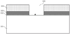
The steps of the existing preparation process of the shallow trench isolation structure are shown in fig. 1 a-1 m, and specifically comprise: an
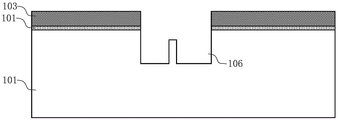
oxide layer 102 and a
silicon nitride layer 103 formed on the surface of the
silicon substrate 101, as shown in FIG. 1a, wherein the total thickness of the
oxide layer 102 and the
silicon nitride layer 103 is 1600 angstroms
Left and right.
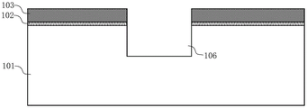
The STI regions are opened using a photo-mask or photoresist 104 and the silicon nitride layer 103 and oxide layer 102 are dry etched to form ST1 windows 105, as shown in fig. 1 b.
The silicon substrate 101 is etched to form a trench 106 having a depth of about 4000 angstroms, as shown in figure 1 c.
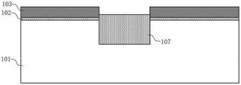
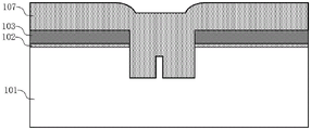
An oxide 107 is deposited on the upper surface of the silicon nitride layer 103 and in the trench 106 as shown in figure 1 d.
CMP (chemical mechanical polishing) of the oxide 107 is used until the upper surface of the oxide 107 in the region of the trench 106 is about 300 a higher than the upper surface of the silicon substrate 101, as shown in figure 1 e.
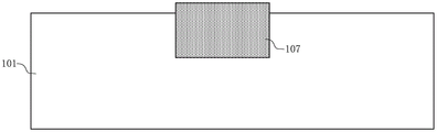
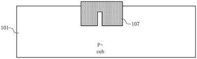
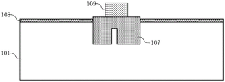
The silicon nitride layer 103 and the oxide layer 102 on the surface of the silicon substrate 101 are removed as shown in fig. 1 f.
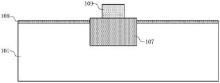
A gate oxide layer 108 is grown on the surface of the silicon substrate 101, and Polysilicon (POLY)109 is formed on a portion of the surface of the oxide 107 in the region of the trench 106 by deposition, exposure, etching, and the like, as shown in fig. 1 g.
However, if there is a defect in the SIN forming the silicon nitride layer 103, the SIN etching rate at the defect is slow, as shown in fig. 1h, in the similar etching process to the window 105 formed in fig. 1b, an oxide layer plus SIN residue (or only an oxide layer residue) is formed, and thus, the process of fig. 1c to 1g becomes the process of fig. 1i to 1m, and finally, under the polysilicon 109, the oxide 107 with the thickness of 4000 angstroms is not completely, and a residual silicon surface is included, which is close to or equal to the thickness of the gate oxide layer 108 at most seriously, so that the isolation effect of the shallow trench isolation structure formed is poor, and the threshold voltage of the transistor is affected, which will result in the reduction of the yield of the product.
In view of the above problems in the prior art, the applicant has made earnest research and analysis to find that the number of defects in silicon nitride is positively correlated to the thickness of the silicon nitride layer, and based on this, the applicant has proposed an improved process for preparing a shallow trench isolation structure, and by reducing the thickness of the silicon nitride layer used in the preparation process of the shallow trench isolation structure, the number of defects in silicon nitride is reduced, thereby achieving the purpose of reducing the number of silicon residues in the shallow trench isolation structure.
In the method for manufacturing a shallow trench isolation structure disclosed in the first embodiment of the present invention, the multilayer structure in which the plurality of oxide layers and the plurality of silicon nitride layers are alternately arranged and the additional silicon nitride sidewall structure are used to replace the structure of the oxide layer 102 and the silicon nitride layer 103 in the existing manufacturing process, that is, under the condition that the total thickness of the multilayer structure in which the plurality of oxide layers and the plurality of silicon nitride layers are alternately arranged is not changed, the additional oxide layer is used to replace a part of the silicon nitride structure in the prior art, so that the thickness of silicon nitride to be etched in the whole manufacturing process is reduced, the number of defects in the silicon nitride layer is reduced, and further, after subsequent etching, the number of silicon residues in the shallow trench isolation structure is greatly reduced. Meanwhile, in the process of forming the groove, the silicon nitride structure is etched twice, so that the thickness of the silicon nitride required to be etched in each etching process is reduced, the residual quantity of silicon in the shallow groove isolation structure can be greatly reduced after the etching is finished, and the product yield is improved. Wherein the overall thickness of the plurality of oxide layers and the plurality of silicon nitride layers in the embodiments of the present invention may be the same as the overall thickness of the oxide layer 102 and the silicon nitride layer 103 shown in fig. 1 a-1 g. As shown in fig. 2, the preparation method disclosed in this embodiment specifically includes the following steps:
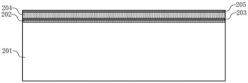
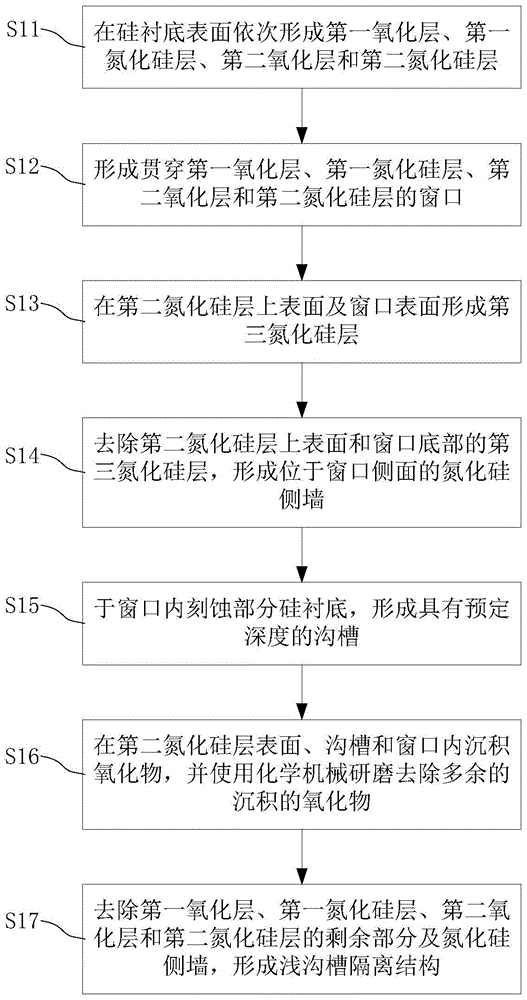
in step S11, a first oxide layer, a first silicon nitride layer, a second oxide layer, and a second silicon nitride layer are sequentially formed on the surface of the silicon substrate.
Illustratively, as shown in fig. 3a, an oxide, such as silicon oxide, is grown on the upper surface of the silicon substrate 201 to form a first oxide layer 202; then depositing silicon nitride on the upper surface of the first oxide layer 202 to form a first silicon nitride layer 203 as thin as possible; then depositing an oxide, such as silicon oxide, on the upper surface of the first silicon nitride layer 203 to form a second oxide layer 204; thereafter, the deposition of silicon nitride is continued on the upper surface of the second oxide layer 204 to form a second silicon nitride layer 205 as thin as possible. The first oxide layer 202 may be formed by a conventional thermal oxidation method or a conventional chemical vapor deposition method, and the first silicon nitride layer 203, the second oxide layer 204, and the second silicon nitride layer 205 may be formed by a conventional chemical vapor deposition method.
In one possible embodiment of the present invention, the thickness of each of the first silicon nitride layer 203 and the second silicon nitride layer 205 is much smaller than the thickness of the second oxide layer 204. Compared with the scheme in the prior art as shown in fig. 1a to fig. 1m, in the preparation process of the shallow trench isolation structure, the second oxide layer 204 is used to replace most of the silicon nitride structures in the prior art under the condition of keeping the total thickness of all the oxide layers and the silicon nitride layer unchanged, so that the thickness of the silicon nitride to be etched is reduced, the number of defects in the silicon nitride layer is reduced, the number of silicon residues in the shallow trench isolation structure is greatly reduced after subsequent etching, and the product yield is improved.
Further, the thickness of the first oxide layer 202 formed in this embodiment is smaller than that of the second oxide layer 204.
In step S12, a window is formed through the first oxide layer, the first silicon nitride layer, the second oxide layer, and the second silicon nitride layer.
Illustratively, as shown in fig. 3b, a photoresist 206 is disposed on the upper surface of the second silicon nitride layer 205, and is exposed to a predetermined trench region using a conventional photolithography process to open an STI window. Thereafter, the first oxide layer 202, the first silicon nitride layer 203, the second oxide layer 204 and the second silicon nitride layer 205 on the STI window region are partially etched away by using a conventional dry etching process, so as to form a window 207 penetrating through the first oxide layer 202, the first silicon nitride layer 203, the second oxide layer 204 and the second silicon nitride layer 205.
It will be appreciated that the etch materials used in etching the oxide and silicon nitride layers separately using conventional dry etch processes are not the same. In the embodiment of the invention, a structure formed by stacking a plurality of oxide layers and a plurality of silicon nitride layers is used as a hard mask, and in the process of etching the window 207, the silicon nitride can be over-etched by adopting a dry etching process with a high proportion (proportion of the dosage of etching materials for the silicon nitride layers and the oxide layers during etching), so that the condition that the surfaces of the adjacent oxide layers have different etching depths after the silicon nitride layers are etched can be ensured to be completely etched even if defects exist in the silicon nitride of the first silicon nitride layer 203 and the second silicon nitride layer 205, and the loss of the adjacent oxide layers is small during etching a certain silicon nitride layer, and the flatness of the bottom of the formed window 207 can be improved.
In step S13, a third silicon nitride layer is formed on the top surface of the second silicon nitride layer and the surface of the window.
Illustratively, as shown in fig. 3c, conventional chemical vapor deposition is used to deposit silicon nitride on the top surface of the second silicon nitride layer 205 and within the window 207 to form a third silicon nitride layer 208 that is as thin as possible.
In one possible embodiment of the present invention, the third silicon nitride layer 208 is also formed to a thickness much smaller than the thickness of the second oxide layer 204. Meanwhile, the total thickness of the first oxide layer 202, the first silicon nitride layer 203, the second oxide layer 204 and the second silicon nitride layer 205 formed on the surface of the silicon substrate 201 in the embodiment of the present invention is 1100 angstroms to 2000 angstroms, for example 1600 angstroms, which is the same as the total thickness of the oxide layer 102 and the silicon nitride layer 103 formed on the surface of the silicon substrate 101 in the prior art scheme as shown in fig. 1a to 1 m. Wherein the thickness of the first oxide layer 202 is 50 to 150 angstroms, for example, 100 angstroms; the sum of the thicknesses of the first silicon nitride layer 203, the second silicon nitride layer 205, and the second oxide layer 204 is formed to be 1000 angstroms to 1800 angstroms, for example, 1500 angstroms.
In step S14, the third silicon nitride layer portions on the top surface of the second silicon nitride layer and the bottom of the window are removed to form silicon nitride spacers on the sides of the window.
Illustratively, as shown in fig. 3d, a conventional dry etching process is used to remove the portion of the third silicon nitride layer on the upper surface of the second silicon nitride layer 205 and the portion of the third silicon nitride layer at the bottom of the window 207 (i.e., the portion of the third silicon nitride layer on the silicon substrate 201 in the window 207), and only the portions of the third silicon nitride layer on both sides of the window 207 are remained, so as to form the silicon nitride sidewall.
In the process of forming the trench 209 according to the embodiment of the present invention, the conventional dry etching process is respectively used in step S12 and step S14 to etch the silicon nitride in the trench region twice (the first silicon nitride layer 203 and the second silicon nitride layer 205 are etched for the first time, and the third silicon nitride layer 208 is etched for the second time), that is, in the method for manufacturing the shallow trench isolation structure shown in the embodiment of the present invention, not only is the overall thickness of the silicon nitride reduced compared with the existing process, but also the dry etching is performed twice on the thinned silicon nitride, so that the thickness of the silicon nitride to be etched in each etching process is also reduced, and thus, the etching effect on the silicon nitride is enhanced, and the amount of silicon residues in the trench region in the shallow trench isolation structure can be further reduced.
In step S15, a portion of the silicon substrate is etched in the window to form a trench having a predetermined depth.
Illustratively, as shown in fig. 3e, a trench 209 having a predetermined depth is formed by etching the portion of the silicon substrate 201 within the window 207 using a conventional dry etch process. In this embodiment, based on the silicon nitride sidewall spacers formed in step S14, the oxide layer (the first oxide layer 202 and the second oxide layer 204) structures on both sides of the trench 209 may be protected from being corroded during the step S15 of performing the longitudinal etching to form the trench 209, which is helpful for maintaining the integrity of the subsequently formed shallow trench isolation structure.
In step S16, an oxide is deposited on the surface of the second silicon nitride layer, in the trenches and in the windows, and the excess deposited oxide is removed using chemical mechanical polishing.
Illustratively, after forming the trench 209, first, as shown in fig. 3f, an oxide 210, such as silicon oxide, is deposited on the surface of the second silicon nitride layer 205, in the trench 209 and in the window 207 by using a conventional chemical vapor deposition method, and then, as shown in fig. 3g, excess deposited oxide 210 is removed by using a conventional chemical mechanical polishing CMP process, so that the height or thickness of the oxide 210 in the trench 209 finally meets the predetermined requirement, for example, in the formed shallow trench isolation structure, the thickness of the portion of the oxide 210 in the trench 209 above the surface of the silicon substrate 201 is 100 a to 500 a, such as 300 a.
In step S17, the remaining portions of the first oxide layer, the first silicon nitride layer, the second oxide layer and the second silicon nitride layer, and the silicon nitride sidewall are removed to form a shallow trench isolation structure.
Exemplarily, as shown in fig. 3h, the remaining portions of the first silicon nitride layer 203 and the second silicon nitride layer 205 and the silicon nitride sidewalls 208 are removed by using a conventional wet etching process, so that the second oxide layer 204 wrapped between the first silicon nitride layer 203, the second silicon nitride layer 205 and the silicon nitride sidewalls 208 is naturally peeled off; and after removing the silicon nitride, removing the first oxide layer 202 using a conventional dry etching or wet etching process to form a shallow trench isolation structure. In this step, an additional step of removing the second oxide layer 204 is not required, which simplifies the preparation process of the shallow trench isolation structure to a certain extent. Meanwhile, the silicon nitride spacers 208 can also protect the oxide 210 in the trench region from being affected during the etching process, which is helpful for maintaining the integrity of the shallow trench isolation structure.
In the method for manufacturing a shallow trench isolation structure disclosed in the second embodiment of the present invention, the thickness of the silicon nitride layer used in the process of manufacturing the shallow trench isolation structure can be reduced by adjusting the thickness ratio of the oxide layer to the silicon nitride layer under the condition that the total thickness of the oxide layer and the silicon nitride layer is not changed (that is, the total thickness of the oxide layer and the silicon nitride layer in the embodiment of the present invention is the same as the total thickness of the oxide layer 102 and the silicon nitride layer 103 shown in fig. 1a to 1 g), so that the number of defects existing in the silicon nitride layer is reduced, and the number of silicon residues in the shallow trench isolation structure can be reduced to a greater extent during subsequent etching. As shown in fig. 4, the preparation method disclosed in this embodiment specifically includes the following steps:
in step S21, an oxide layer and a silicon nitride layer are sequentially formed on the surface of the silicon substrate.
Illustratively, as shown in fig. 5a, an oxide, such as silicon oxide, is deposited on the upper surface of a silicon substrate 301 by conventional chemical vapor deposition to form an oxide layer 302; silicon nitride is then deposited on the top surface of oxide layer 302 using a conventional chemical vapor deposition process to form silicon nitride layer 303. The thickness of the silicon nitride layer 303 formed in this embodiment is equivalent to the thickness of the oxide on the surface of the silicon substrate 301 in the finally formed shallow trench isolation structure. For example, in one possible embodiment of the present invention, the absolute value of the difference between the thickness of the silicon nitride layer 303 after chemical mechanical polishing and the thickness of the oxide layer on the surface of the silicon substrate 301 in the finally formed shallow trench isolation structure is less than 100 angstroms.
In one possible embodiment of the present invention, the total thickness of the oxide layer 302 and the silicon nitride layer 303 formed on the surface of the silicon substrate 301 is 1100 a to 2000 a, for example 1600 a, which is the same as the total thickness of the oxide layer 102 and the silicon nitride layer 103 formed on the surface of the silicon substrate 101 in the prior art solution as shown in fig. 1a to 1 m. The thickness of the oxide layer 302 formed in this embodiment is, for example, 1100 a to 1900 a, and the thickness of the silicon nitride layer 303 formed in this embodiment is, for example, 100 a to 500 a, that is, the thickness of the silicon nitride layer formed in this embodiment is smaller than the thickness of the oxide layer 302 formed. According to the invention, the thickness ratio of the oxide layer 302 to the silicon nitride layer 303 is adjusted in the preparation process of the shallow trench isolation structure, so that the thickness of the used silicon nitride is reduced, and the number of defects in the silicon nitride layer is reduced.
In step S22, a window is formed through the oxide layer and the silicon nitride layer.
Illustratively, as shown in fig. 5b, a photoresist 304 is disposed on the upper surface of the silicon nitride layer 303, and is exposed in a predetermined trench region using a conventional photolithography process to open an STI window. Thereafter, portions of the oxide layer 302 and the silicon nitride layer 303 are etched away over the STI window region using a conventional dry etch process to form a window 305 through the oxide layer 302 and the silicon nitride layer 303.
In step S23, a portion of the silicon substrate is etched in the window to form a trench having a predetermined depth.
Illustratively, as shown in FIG. 5c, a trench 306 having a predetermined depth is formed by etching a portion of the silicon substrate 301 within the window 305 using a conventional dry etch process.
In step S24, an oxide is deposited on the surface of the silicon nitride layer, in the trench and in the window, and a chemical mechanical polishing is used to remove the excess deposited oxide, so that the upper surface of the oxide in the trench region after the chemical mechanical polishing is flush with the upper surface of the silicon nitride layer.
Illustratively, after forming trench 306, an oxide 307, such as silicon oxide, is first deposited on the surface of silicon nitride layer 303, within trench 306 and window 305 using a conventional chemical vapor deposition process, as shown in fig. 5 d. The excess deposited oxide 307 is then removed using a conventional CMP process, as shown in fig. 5e, so that the top surface of the oxide 307 in the region of the trench 306 is flush with the top surface of the silicon nitride layer 303 after CMP. Compared with the prior art in which the surface of the oxide 307 needs to be polished to be lower than the upper surface of the silicon nitride layer 303, the embodiment of the present invention is based on the thickness of the silicon nitride layer 303, so that only the surface of the oxide 307 needs to be polished to be flush with the upper surface of the silicon nitride layer 303 or have a difference smaller than a predetermined value (which can be understood by referring to the following description specifically), thereby reducing the complexity of the chemical polishing process operation and optimizing the preparation process of the shallow trench isolation structure.
In this embodiment, the oxide layer 302 is formed of the same material as the oxide 307 grown in the trench 306.
In step S25, the remaining portion of the silicon nitride layer is removed using a wet etch.
Illustratively, as shown in fig. 5f, the silicon nitride layer 303 is removed using a conventional wet etch process. It is understood that, since the upper surface of the oxide 307 in the trench 306 region after the chemical mechanical polishing in this embodiment is flush with the upper surface of the silicon nitride layer 303, and the thickness of the silicon nitride layer 303 formed in this embodiment is equivalent to the thickness of the portion of the finally formed shallow trench isolation structure where the oxide 307 is located above the surface of the silicon substrate 301, after the silicon nitride layer 303 is etched in step S25, the thickness of the portion of the oxide 307 located above the surface of the oxide layer 302 is the required thickness of the portion of the finally formed shallow trench isolation structure where the oxide 307 is located above the surface of the silicon substrate 301.
In step S26, the remaining portion of the oxide layer and the oxide layer are dry etched until the remaining portion of the oxide layer is removed to form a shallow trench isolation structure.
Illustratively, as shown in fig. 5g, the oxide layer 302 on the surface of the silicon substrate 301 is removed by a conventional dry etching process. It is understood that since the oxide layer 302 is formed of the same material as the oxide 307 grown in the trench 306, the oxide 307 is etched to the same thickness as the oxide layer 302 during the dry etching process, and further, in the shallow trench isolation structure formed after completely etching the oxide layer 302, the thickness of the portion of the oxide 307 on the surface of the silicon substrate 301 is the required thickness.
It should be noted that the numerical values listed in the embodiments of the present invention are merely exemplary, and should not be construed as limiting the present invention.
In conclusion, the preparation process of the shallow trench isolation structure is optimized, the silicon residue in the shallow trench isolation structure can be greatly reduced under the condition that the defect density in the unit volume of the silicon nitride is not changed, and the product yield is improved.
Finally, it should be noted that: it should be understood that the above examples are only for clearly illustrating the present invention and are not intended to limit the embodiments. Other variations and modifications will be apparent to persons skilled in the art in light of the above description. And are neither required nor exhaustive of all embodiments. And obvious variations or modifications of the invention may be made without departing from the scope of the invention.