CN114309987A - Laser cutting method and device for display panel - Google Patents
Laser cutting method and device for display panel Download PDFInfo
- Publication number
- CN114309987A CN114309987A CN202210036686.4A CN202210036686A CN114309987A CN 114309987 A CN114309987 A CN 114309987A CN 202210036686 A CN202210036686 A CN 202210036686A CN 114309987 A CN114309987 A CN 114309987A
- Authority
- CN
- China
- Prior art keywords
- cutting
- laser
- glass substrate
- full
- display panel
- Prior art date
- Legal status (The legal status is an assumption and is not a legal conclusion. Google has not performed a legal analysis and makes no representation as to the accuracy of the status listed.)
- Pending
Links
Images


Abstract
The invention discloses a laser cutting method and device for a display panel, which are used for cutting a large-size OLED (organic light emitting diode) motherboard material with a two-layer structure and a glass substrate, and the method comprises the following steps: performing full-cutting on the flexible layer by using a CO2 laser until the glass substrate layer below the flexible layer is exposed; carrying out wire-forming cutting on the glass substrate layer along a cutting channel formed by full cutting by using an ultrafast laser; the glass substrate layer after the wire cutting was irradiated with a CO2 laser and split. The invention simplifies the process flow of the equipment, reduces the requirements on the mechanical lobe device and the mechanical lobe positioning, and reduces the volume of the equipment and the production cost.
Description
Technical Field
The invention relates to the technical field of laser processing, in particular to laser cutting of a display panel with a glass substrate, and specifically relates to a laser cutting method and device of the display panel.
Background
The Laser processing flow of the flexible OLED display panel is mainly divided into two types, and the difference is the sequence of Laser Lift-Off (Laser Lift-Off) and Laser fragmentation (Laser segmentation):
panel LLO, directly carrying out laser stripping on a mother board with glass, then carrying out rough cutting on the mother board by small pieces, and finally carrying out die set and fine cutting on each CELL.
CELL LLO, firstly carrying out laser slicing rough cutting on a mother board with a glass substrate, then carrying out small-piece peeling, and finally carrying out module group and fine cutting on each CELL.
A typical stacked structure of a mother-board OLED with a glass substrate is shown in fig. 1. For the laser cutting of a mother board with a glass substrate in a Cell LLO process, there are three existing cutting methods: (1) cutting was performed using only a CO2 laser; (2) cutting with ultrafast laser only; (3) cutting was performed using a CO2 laser in combination with an ultrafast laser.
The results of all three cutting modes were: cutting all flexible materials such as PET, TFE, OLED, TFT and PI, half-cutting substrate glass, and mechanically splitting to realize separation.
For a large-size mother board, strip cutting and splitting are generally performed to divide the mother board into a plurality of strips, and then unit cutting and splitting are performed on the strip mother board to finally obtain unit chips with specified sizes. Fig. 2 shows a specific process flow diagram of laser slicing of an OLED motherboard with a glass substrate, which is widely used at present, wherein laser bar cutting and mechanical bar breaking are two separate processing areas on one device, and require relatively complex mechanisms such as mechanical handling, mechanical transmission, rotational positioning compensation, and similarly, laser unit cutting and mechanical unit breaking are similar processes and structures.
The difference between the three cutting modes:
(1) and only CO2 laser is used for cutting, so that the cost is low, the cutting quality is general, a larger cutting path needs to be reserved when the cutting groove is wider, and the heat influence is larger.
(2) Only ultrafast laser cutting is used, picosecond ultraviolet or femtosecond laser is generally used, the cost is high, the cutting quality of most materials is good, but the quality is general when materials such as PET are cut, a cutting groove is small, and the heat influence is small.
(3) The cutting method has the advantages that the cutting is carried out in the cooperation of the CO2 laser and the ultrafast laser, the ultrafast laser generally uses picosecond ultraviolet or even femtosecond laser, the cost is highest, different laser light sources are used for cutting aiming at different material types, the cutting quality is good, the cutting groove is small, and the heat influence is small.
In order to ensure good cutting quality, the third type is mostly used in the market at present, but even the third type has some problems: the cost is too high, and the steps of mechanical transmission, mechanical splitting and the like are still needed after cutting. Particularly, the need for mechanical breaking requires not only a larger and more complicated automated mechanical breaking apparatus, increasing the overall size and complexity of the equipment, thereby increasing cost and maintenance difficulties, but also increasing the production time per unit product.
Disclosure of Invention
To overcome the above-mentioned deficiencies of the prior art, the present invention provides a method and an apparatus for laser cutting a display panel, which are used to solve at least one of the above-mentioned technical problems.
According to an aspect of the present specification, there is provided a display panel laser cutting method for cutting a large-sized OLED mother sheet material with a glass substrate in a two-layer structure, the method including:
performing full-cutting on the flexible layer by using a CO2 laser until the glass substrate layer below the flexible layer is exposed;
carrying out wire-forming cutting on the glass substrate layer along a cutting channel formed by full cutting by using an ultrafast laser;
the glass substrate layer after the wire cutting was irradiated with a CO2 laser and split.
According to the technical scheme, for the large-size OLED mother board material with the glass substrate and the two-layer structure, the strip-shaped cutting and splitting and the unit cutting and splitting of the sample material are sequentially completed according to the sequence of CO2 laser full cutting, ultrafast laser filament forming cutting and CO2 laser irradiation splitting, and the complete CO2 laser full cutting, ultrafast laser filament forming cutting and CO2 laser irradiation splitting processes are completed at the same station, so that the strip-shaped cutting and splitting and the unit cutting and splitting processes of the display panel can be completed only by two stations, and the equipment process flow is simplified; meanwhile, as the splitting process is carried out at the laser cutting station, the requirements for a mechanical splitting device and mechanical splitting positioning are reduced, and the volume of the equipment is reduced.
As a further technical scheme, the CO2 laser is matched with a moving platform or a galvanometer scanning system to perform laser full-cutting on the flexible layer. The motion platform drives the processing sample to move, and the CO2 laser is used for cutting the flexible layer completely; or, the CO2 laser is moved by a galvanometer scanning system to complete the full-cutting of the flexible layer.
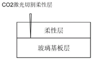
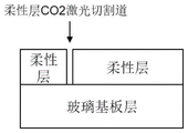
As a further technical scheme, the full-cutting forms a cutting channel of 180-220um on the flexible layer, and the cutting channel extends to the surface of the glass substrate layer. The flexible layer material on the cutting channel is completely removed by full cutting, so that the glass substrate material is exposed and is not damaged.
As a further technical scheme, the ultrafast laser is matched with a filamentation cutting head or a bessel cutting head to carry out filamentation cutting on the glass substrate layer. After the flexible layer material is removed by CO2 laser, the cutting processing of the brittle transparent materials such as glass, sapphire and the like of the substrate part is realized by adopting a picosecond infrared laser matched with a cutting head such as wire forming and Bessel.
As a further technical scheme, the CO2 laser is matched with a motion platform or a galvanometer scanning system to heat and split a cutting track formed by filamentation cutting.
According to one aspect of the specification of the invention, the laser cutting equipment for the display panel is used for cutting a large-size OLED mother board material with a two-layer structure and a glass substrate and comprises a control device, wherein the control device is respectively connected with a carrying device and two groups of laser processing devices, and the two groups of laser processing devices are respectively arranged in two laser processing areas; the conveying device is used for conveying the processing sample from one laser processing area to another laser processing area; each group of laser processing devices comprises a CO2 laser and an ultrafast laser; the CO2 laser is used for carrying out full-cutting on the flexible layer until the glass substrate layer below the flexible layer is exposed; the ultrafast laser is used for performing filamentation cutting on the glass substrate layer along a cutting channel formed by full-cutting; the CO2 laser is also used for irradiation splintering of the glass substrate layer after the filamentation and cutting.
According to the technical scheme, the laser cutting and the splitting are integrated at one station, and after the CO2 laser full cutting is carried out, the filamentation cutting and the CO2 laser splitting are carried out in sequence, so that the laser slicing cutting quality can be obviously improved, and the edge breakage generated during the glass cutting and splitting is reduced; meanwhile, as the laser cutting and splitting are completed in the same processing area, the mechanical splitting and the mechanical splitting positioning are omitted, and the mechanical transmission and auxiliary equipment required by the fact that the laser cutting and the splitting are located at different stations are omitted, only one process is needed to be added during the laser cutting, so that the process difficulty is greatly reduced, the equipment volume is reduced, and the equipment production flow is simplified.
As a further technical scheme, the two laser processing areas are a laser strip cutting and lobe splitting processing area and a laser unit cutting and lobe splitting processing area respectively. The two processing areas have the same processes of CO2 laser full cutting, ultrafast laser filamentation cutting and CO2 laser splinting, and the whole production process of the equipment is simplified.
As a further technical scheme, the ultrafast laser is a picosecond infrared laser. After the flexible layer material is removed by CO2 laser, the cutting processing of the brittle transparent materials such as glass, sapphire and the like on the substrate part is realized by adopting a picosecond infrared laser to match with cutting heads such as filamentation and Bessel and the like, and compared with the traditional picosecond ultraviolet or femtosecond laser, the equipment cost is reduced.
As a further technical scheme, the system is further provided with a moving platform or a galvanometer scanning system and is used for being matched with a CO2 laser to achieve full-cutting of the flexible layer.
As a further technical solution, the ultrafast laser is configured with a wire-forming cutting head or a bessel cutting head for performing wire-forming cutting on a glass substrate layer.
Compared with the prior art, the invention has the beneficial effects that:
(1) the invention provides a method, aiming at a large-size OLED mother board material with a two-layer structure and a glass substrate, the method sequentially finishes strip-shaped cutting and splitting and unit cutting and splitting of a sample material according to the sequence of CO2 laser full cutting, ultrafast laser filament forming cutting and CO2 laser irradiation splitting, and finishes the complete CO2 laser full cutting, ultrafast laser filament forming cutting and CO2 laser irradiation splitting processes at one time at the same station, so that the strip-shaped cutting and splitting and the unit cutting and splitting processes of a display panel can be finished only by two stations, and the process flow of equipment is simplified; meanwhile, as the splitting process is carried out at the laser cutting station, the requirements for a mechanical splitting device and mechanical splitting positioning are reduced, and the volume of the equipment is reduced.
(2) The invention provides equipment, which integrates laser cutting and splitting at a station, and sequentially performs filamentation cutting and CO2 laser splitting after CO2 laser full cutting, so that the cutting quality of laser splitting can be obviously improved, and edge breakage generated during glass cutting and splitting is reduced; meanwhile, as the laser cutting and splitting are completed in the same processing area, the mechanical splitting and the mechanical splitting positioning are omitted, and the mechanical transmission and auxiliary equipment required by the fact that the laser cutting and the splitting are located at different stations are omitted, only one process is needed to be added during the laser cutting, so that the process difficulty is greatly reduced, the equipment volume is reduced, and the equipment production flow is simplified.
Drawings
Fig. 1 is a schematic diagram of a typical lamination structure of an OLED motherboard with a glass substrate.
Fig. 2 is a flow chart of a conventional laser slicing process of an OLED mother substrate with a glass substrate.
Fig. 3 is a flowchart of a laser cleaving process of an OLED mother substrate with a glass substrate according to an embodiment of the present invention.
FIG. 4 is a schematic diagram of a CO2 laser cut flexible layer according to an embodiment of the present invention.
Fig. 5 is a schematic diagram of a cutting path left after CO2 full cutting according to an embodiment of the present invention.
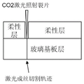
FIG. 6 is a schematic diagram of ultrafast laser filamentation cutting according to an embodiment of the present invention.
Fig. 7 is a schematic diagram of CO2 laser irradiation fragmentation according to an embodiment of the present invention.
Detailed Description
The technical solutions of the embodiments of the present invention will be described clearly and completely with reference to the accompanying drawings, and it is to be understood that the described embodiments are only a part of the embodiments of the present invention, and not all of the embodiments. All other embodiments, which can be derived by a person skilled in the art from the embodiments of the present invention without any inventive step, are within the scope of the present invention.
The invention provides a laser cutting method for a display panel, which is used for cutting a large-size OLED (organic light emitting diode) motherboard material with a two-layer structure and a glass substrate. The large-size OLED mother board material with the glass substrate can be structurally divided into two layers, namely a flexible layer and a rigid glass substrate layer, wherein the flexible layer comprises a PET, TFE, OLED, TFT, PI and other laminated structures and serves as a finally needed display panel part, and the glass substrate layer is an additional material discarded after stripping.
The whole processing process of the invention uses two lasers, namely a picosecond infrared ultrafast laser and a CO2 laser.
As shown in fig. 3-6, the laser cutting method proposed by the present invention is divided into three steps: step 1, carrying out laser full-cutting processing on a flexible layer material by a CO2 laser in cooperation with a motion platform or a galvanometer scanning system to form a cutting channel about 200um, and completely removing the flexible layer material on the cutting channel to expose and not damage a bottom transparent glass substrate material; step 2, along the cutting path formed in the step 1, a picosecond infrared ultrafast laser is matched with a cutting head such as a filamentation head and a Bessel cutting head to be used for carrying out filamentation cutting on the transparent glass substrate material; and 3, heating and splitting the cutting track of the filamentation cutting by the CO2 laser in cooperation with a motion platform or a galvanometer scanning system, and finally achieving the purpose of splitting the mother board.
The method for performing filament cutting and CO2 laser splitting on the glass substrate material in the steps 2 and 3 can obviously improve the cutting quality of laser splitting, reduce edge breakage generated during glass cutting and splitting, and simultaneously, the laser cutting equipment can save mechanical transmission, sample positioning and mechanical splitting parts and only needs to add one process during laser processing. The method described by the invention is laser processing for three times, namely CO2 laser, ultrafast laser and CO2 laser are processed one time in sequence, and the ultrafast laser used for filamentation cutting only needs to use a picosecond infrared laser, so that the method has the advantage of reducing the cost compared with a picosecond ultraviolet or femtosecond laser in the original method. The method has the advantages of simplifying the production flow of the equipment, reducing the volume of the equipment, reducing the process difficulty, improving the production efficiency and the like, and reduces the equipment and operation cost.
According to an aspect of the present specification, there is provided a display panel laser cutting apparatus for cutting a large-sized OLED mother substrate material with a glass substrate in a two-layer structure.
The cutting equipment comprises a control device, the control device is respectively connected with a carrying device and two groups of laser processing devices, and the two groups of laser processing devices are respectively arranged in two laser processing areas; the conveying device is used for conveying the processing sample from one laser processing area to another laser processing area; each group of laser processing devices comprises a CO2 laser and an ultrafast laser; the CO2 laser is used for carrying out full-cutting on the flexible layer until the glass substrate layer below the flexible layer is exposed; the ultrafast laser is used for performing filamentation cutting on the glass substrate layer along a cutting channel formed by full-cutting; the CO2 laser is also used for irradiation splintering of the glass substrate layer after the filamentation and cutting.
The two laser processing areas are respectively a laser strip cutting and lobe splitting processing area and a laser unit cutting and lobe splitting processing area.
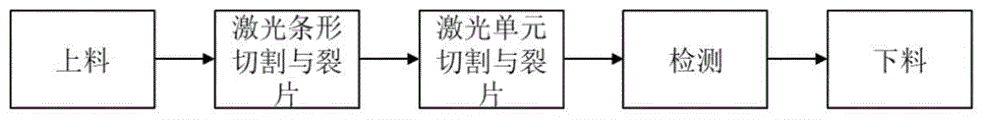
Fig. 7 shows a cutting process of the apparatus of the present invention, in which the processes of loading, detecting and unloading are the same as those of the prior art, and laser bar cutting and splitting, and laser unit cutting and splitting are implemented in respective laser processing regions.
The laser machining area is a double-head machining area and comprises a CO2 laser and an ultrafast laser, wherein the ultrafast laser is configured with a filamentation cutting head or a Bessel cutting head. The equipment can save mechanical transmission, mechanical splinters and auxiliary mechanisms thereof, laser processing and laser splinters are finished in the laser processing area, and the laser double-head processing area is arranged at the same position, so that the production flow can be simplified, the volume of the equipment can be reduced, the processing time can be reduced, the equipment and the production cost can be reduced, and the processing efficiency can be improved.
For laser bar cutting and splitting, the processing flow is divided into three steps: CO2 laser cuts the flexible layer completely exposing the underlying glass substrate layer; carrying out filamentation cutting on the transparent glass substrate layer on a CO2 laser cutting channel by ultrafast laser; the CO2 laser irradiates the glass substrate layer on the filamentation cutting path to split. After the laser processing area is processed, the laser processing area is directly conveyed to the laser unit cutting and splitting area by the mechanical conveying device, and similarly, the laser unit cutting and splitting area is similar in flow and structure.
The processing flow of the invention only needs to be positioned once, the positioning processing precision is ensured by the carrying device and the control device, and the positioning process of the existing splinter mechanism is omitted.
The system is also provided with a moving platform or a galvanometer scanning system and is used for matching with a CO2 laser to realize the full-cutting of the flexible layer.
Further, the moving platform drives the sample to move in two processing areas, and the sample is used for being matched with a CO2 laser to realize full-cutting of the flexible layer and being matched with a CO2 laser to realize heating splitting of a cutting track formed by filamentation cutting. The foregoing process can also be accomplished by the cooperation of a galvanometer scanning system with a CO2 laser.
The cutting method and the cutting equipment provided by the invention are used for the large-size OLED motherboard material with the glass substrate, the cutting quality can be improved, the cutting process and the equipment complexity are simplified, the production cost is reduced, and the processing efficiency is improved.
Finally, it should be noted that: the above examples are only intended to illustrate the technical solution of the present invention, but not to limit it; although the present invention has been described in detail with reference to the foregoing embodiments, it will be understood by those of ordinary skill in the art that: the technical solutions described in the foregoing embodiments may still be modified, or some or all of the technical features may be equivalently replaced; and the modifications or the substitutions do not make the essence of the corresponding technical solutions deviate from the technical solutions of the embodiments of the present invention.
Claims (10)
1. A laser cutting method for a display panel, which is used for cutting a large-size OLED (organic light emitting diode) motherboard material with a two-layer structure and a glass substrate, and is characterized by comprising the following steps:
performing full-cutting on the flexible layer by using a CO2 laser until the glass substrate layer below the flexible layer is exposed;
carrying out wire-forming cutting on the glass substrate layer along a cutting channel formed by full cutting by using an ultrafast laser;
the glass substrate layer after the wire cutting was irradiated with a CO2 laser and split.
2. The laser cutting method for the display panel according to claim 1, wherein the CO2 laser is used in cooperation with a motion platform or a galvanometer scanning system to perform laser full-cut cutting on the flexible layer.
3. The laser cutting method for display panel according to claim 2, wherein the full-cut cutting is performed on the flexible layer to form a cutting channel of 180-220um, and the cutting channel extends to the surface of the glass substrate layer.
4. The laser cutting method for display panel according to claim 1, wherein the ultrafast laser is used in combination with a filament-forming cutting head or a Bessel cutting head to perform filament-forming cutting on the glass substrate layer.
5. The laser cutting method for the display panel according to claim 1, wherein the CO2 laser is used in cooperation with a motion platform or a galvanometer scanning system to perform heating and splitting on a cutting track formed by filamentation cutting.
6. A display panel laser cutting device is used for cutting a large-size OLED mother board material with a two-layer structure and a glass substrate and is characterized by comprising a control device, wherein the control device is respectively connected with a carrying device and two groups of laser processing devices, and the two groups of laser processing devices are respectively arranged in two laser processing areas; the conveying device is used for conveying the processing sample from one laser processing area to another laser processing area; each group of laser processing devices comprises a CO2 laser and an ultrafast laser; the CO2 laser is used for carrying out full-cutting on the flexible layer until the glass substrate layer below the flexible layer is exposed; the ultrafast laser is used for performing filamentation cutting on the glass substrate layer along a cutting channel formed by full-cutting; the CO2 laser is also used for irradiation splintering of the glass substrate layer after the filamentation and cutting.
7. The laser cutting apparatus for display panel according to claim 6, wherein the two laser processing areas are a laser bar cutting and splitting processing area and a laser unit cutting and splitting processing area, respectively.
8. The laser cutting apparatus for display panels as claimed in claim 6, wherein the ultrafast laser is a picosecond infrared laser.
9. The laser cutting device for display panels as claimed in claim 6, wherein the system is further provided with a moving platform or a galvanometer scanning system for realizing full-cut cutting of the flexible layer in cooperation with a CO2 laser.
10. The laser cutting apparatus for display panels as claimed in claim 6, wherein the ultrafast laser is configured with a wire-forming cutting head or a bessel cutting head for wire-forming cutting of the glass substrate layer.
Priority Applications (1)
| Application Number | Priority Date | Filing Date | Title |
|---|---|---|---|
| CN202210036686.4A CN114309987A (en) | 2022-01-13 | 2022-01-13 | Laser cutting method and device for display panel |
Applications Claiming Priority (1)
| Application Number | Priority Date | Filing Date | Title |
|---|---|---|---|
| CN202210036686.4A CN114309987A (en) | 2022-01-13 | 2022-01-13 | Laser cutting method and device for display panel |
Publications (1)
| Publication Number | Publication Date |
|---|---|
| CN114309987A true CN114309987A (en) | 2022-04-12 |
Family
ID=81025928
Family Applications (1)
| Application Number | Title | Priority Date | Filing Date |
|---|---|---|---|
| CN202210036686.4A Pending CN114309987A (en) | 2022-01-13 | 2022-01-13 | Laser cutting method and device for display panel |
Country Status (1)
| Country | Link |
|---|---|
| CN (1) | CN114309987A (en) |
Cited By (1)
| Publication number | Priority date | Publication date | Assignee | Title |
|---|---|---|---|---|
| CN115521053A (en) * | 2022-10-25 | 2022-12-27 | 深圳市益铂晶科技有限公司 | Fixed-point heating splitting method for glass laser cutting |
Citations (14)
| Publication number | Priority date | Publication date | Assignee | Title |
|---|---|---|---|---|
| CN103811682A (en) * | 2012-11-14 | 2014-05-21 | 乐金显示有限公司 | Method Of Cutting Flexible Display Device And Method Of Fabricating Flexible Display Device Using The Same |
| US20150165563A1 (en) * | 2013-12-17 | 2015-06-18 | Corning Incorporated | Stacked transparent material cutting with ultrafast laser beam optics, disruptive layers and other layers |
| CN104741796A (en) * | 2015-04-20 | 2015-07-01 | 京东方科技集团股份有限公司 | Liquid crystal display panel and manufacturing method thereof and display device |
| CN107931845A (en) * | 2017-11-20 | 2018-04-20 | 武汉华星光电半导体显示技术有限公司 | Cutting method |
| CN108705213A (en) * | 2018-08-08 | 2018-10-26 | 广东正业科技股份有限公司 | A kind of laser processing and device |
| CN108890123A (en) * | 2018-06-25 | 2018-11-27 | 武汉华星光电半导体显示技术有限公司 | A kind of device systems and its operating method of integrated laser removing and laser cutting |
| CN109702356A (en) * | 2019-01-09 | 2019-05-03 | 蓝思智能机器人(长沙)有限公司 | A method of laser cutting covering protection film glass |
| CN209969874U (en) * | 2019-03-21 | 2020-01-21 | 英诺激光科技股份有限公司 | Laser cutting system for ground glass |
| CN110746104A (en) * | 2019-10-31 | 2020-02-04 | 南京赢羊光子科技有限公司 | Cutting and splitting method and system for laser precision processing glass |
| CN210789658U (en) * | 2019-07-30 | 2020-06-19 | 武汉先河激光技术有限公司 | Laser cutting device for mobile phone display screen |
| CN111453982A (en) * | 2020-04-02 | 2020-07-28 | 大族激光科技产业集团股份有限公司 | Method for cutting glass material by laser |
| CN211111717U (en) * | 2019-10-31 | 2020-07-28 | 南京赢羊光子科技有限公司 | Cutting and splitting system for laser precision processing glass |
| CN112846530A (en) * | 2020-12-29 | 2021-05-28 | 武汉华工激光工程有限责任公司 | Curved thick glass cutting and splitting method and system |
| CN113333967A (en) * | 2021-06-04 | 2021-09-03 | 浙江华工光润智能装备技术有限公司 | Splitting method and splitting device for laser cutting of glass |
-
2022
- 2022-01-13 CN CN202210036686.4A patent/CN114309987A/en active Pending
Patent Citations (14)
| Publication number | Priority date | Publication date | Assignee | Title |
|---|---|---|---|---|
| CN103811682A (en) * | 2012-11-14 | 2014-05-21 | 乐金显示有限公司 | Method Of Cutting Flexible Display Device And Method Of Fabricating Flexible Display Device Using The Same |
| US20150165563A1 (en) * | 2013-12-17 | 2015-06-18 | Corning Incorporated | Stacked transparent material cutting with ultrafast laser beam optics, disruptive layers and other layers |
| CN104741796A (en) * | 2015-04-20 | 2015-07-01 | 京东方科技集团股份有限公司 | Liquid crystal display panel and manufacturing method thereof and display device |
| CN107931845A (en) * | 2017-11-20 | 2018-04-20 | 武汉华星光电半导体显示技术有限公司 | Cutting method |
| CN108890123A (en) * | 2018-06-25 | 2018-11-27 | 武汉华星光电半导体显示技术有限公司 | A kind of device systems and its operating method of integrated laser removing and laser cutting |
| CN108705213A (en) * | 2018-08-08 | 2018-10-26 | 广东正业科技股份有限公司 | A kind of laser processing and device |
| CN109702356A (en) * | 2019-01-09 | 2019-05-03 | 蓝思智能机器人(长沙)有限公司 | A method of laser cutting covering protection film glass |
| CN209969874U (en) * | 2019-03-21 | 2020-01-21 | 英诺激光科技股份有限公司 | Laser cutting system for ground glass |
| CN210789658U (en) * | 2019-07-30 | 2020-06-19 | 武汉先河激光技术有限公司 | Laser cutting device for mobile phone display screen |
| CN110746104A (en) * | 2019-10-31 | 2020-02-04 | 南京赢羊光子科技有限公司 | Cutting and splitting method and system for laser precision processing glass |
| CN211111717U (en) * | 2019-10-31 | 2020-07-28 | 南京赢羊光子科技有限公司 | Cutting and splitting system for laser precision processing glass |
| CN111453982A (en) * | 2020-04-02 | 2020-07-28 | 大族激光科技产业集团股份有限公司 | Method for cutting glass material by laser |
| CN112846530A (en) * | 2020-12-29 | 2021-05-28 | 武汉华工激光工程有限责任公司 | Curved thick glass cutting and splitting method and system |
| CN113333967A (en) * | 2021-06-04 | 2021-09-03 | 浙江华工光润智能装备技术有限公司 | Splitting method and splitting device for laser cutting of glass |
Non-Patent Citations (1)
| Title |
|---|
| 肖海兵 主编: "《激光沉积成形增材制造技术》", 华中科学技术大学出版社 * |
Cited By (1)
| Publication number | Priority date | Publication date | Assignee | Title |
|---|---|---|---|---|
| CN115521053A (en) * | 2022-10-25 | 2022-12-27 | 深圳市益铂晶科技有限公司 | Fixed-point heating splitting method for glass laser cutting |
Similar Documents
| Publication | Publication Date | Title |
|---|---|---|
| US9021837B2 (en) | Method of cleaving and separating a glass sheet and apparatus for cleaving and separating a glass sheet | |
| US9010154B2 (en) | Method of cleaving and separating a glass sheet | |
| TWI405732B (en) | A substrate cutting system, a substrate manufacturing apparatus, a substrate scribing method, and a substrate segmentation method | |
| KR101490643B1 (en) | Plate glass scoring and cutting device | |
| CN1645563A (en) | Semiconductor wafer processing method | |
| CN114309987A (en) | Laser cutting method and device for display panel | |
| CN107931845B (en) | Cutting method | |
| US20180342408A1 (en) | Workpiece processing method | |
| US20200079679A1 (en) | Glass film production method | |
| TW201441168A (en) | Substrate processing system and substrate processing method | |
| KR20140142224A (en) | Glass film fracturing method and glass film laminate body | |
| CN113649701A (en) | Solar cell laser edge cleaning method and device | |
| JP2017014032A (en) | Scribe method and scribe device | |
| CN108735918B (en) | Apparatus and method for manufacturing flexible device | |
| KR102136149B1 (en) | Method of manufacturing flexible organic electro luminescence dispaly | |
| JP2002110588A (en) | Chip manufacturing apparatus | |
| CN114496882A (en) | Preparation method of flexible display device | |
| JP2001274441A (en) | Method for collectively cutting solar battery panel | |
| KR102179151B1 (en) | Method of manufacturing flexible organic electro luminescence dispaly | |
| CN220642925U (en) | Ultra-thin cover glass edge etching system | |
| JP2014214054A (en) | Laminated substrate processing device | |
| KR102204685B1 (en) | Method of manufacturing flexible organic electro luminescence dispaly | |
| KR102212175B1 (en) | Method of manufacturing flexible organic electro luminescence dispaly | |
| KR20230023378A (en) | Solar module partial peeling device using multi grinding module | |
| CN116175791A (en) | Splitting method for cutting LED wafer |
Legal Events
| Date | Code | Title | Description |
|---|---|---|---|
| PB01 | Publication | ||
| PB01 | Publication | ||
| SE01 | Entry into force of request for substantive examination | ||
| SE01 | Entry into force of request for substantive examination |