CN1112838C - Ceramic composite wiring structure for semiconductor devices and method of manufacture thereof - Google Patents
Ceramic composite wiring structure for semiconductor devices and method of manufacture thereof Download PDFInfo
- Publication number
- CN1112838C CN1112838C CN97181620A CN97181620A CN1112838C CN 1112838 C CN1112838 C CN 1112838C CN 97181620 A CN97181620 A CN 97181620A CN 97181620 A CN97181620 A CN 97181620A CN 1112838 C CN1112838 C CN 1112838C
- Authority
- CN
- China
- Prior art keywords
- network
- ceramic substrate
- electric
- heat supply
- electric conductor
- Prior art date
- Legal status (The legal status is an assumption and is not a legal conclusion. Google has not performed a legal analysis and makes no representation as to the accuracy of the status listed.)
- Expired - Fee Related
Links
Images


Classifications
-
- H—ELECTRICITY
- H01—ELECTRIC ELEMENTS
- H01L—SEMICONDUCTOR DEVICES NOT COVERED BY CLASS H10
- H01L21/00—Processes or apparatus adapted for the manufacture or treatment of semiconductor or solid state devices or of parts thereof
- H01L21/02—Manufacture or treatment of semiconductor devices or of parts thereof
- H01L21/04—Manufacture or treatment of semiconductor devices or of parts thereof the devices having at least one potential-jump barrier or surface barrier, e.g. PN junction, depletion layer or carrier concentration layer
- H01L21/48—Manufacture or treatment of parts, e.g. containers, prior to assembly of the devices, using processes not provided for in a single one of the subgroups H01L21/06 - H01L21/326
- H01L21/4814—Conductive parts
- H01L21/4846—Leads on or in insulating or insulated substrates, e.g. metallisation
- H01L21/4857—Multilayer substrates
-
- H—ELECTRICITY
- H01—ELECTRIC ELEMENTS
- H01L—SEMICONDUCTOR DEVICES NOT COVERED BY CLASS H10
- H01L23/00—Details of semiconductor or other solid state devices
- H01L23/34—Arrangements for cooling, heating, ventilating or temperature compensation ; Temperature sensing arrangements
- H01L23/36—Selection of materials, or shaping, to facilitate cooling or heating, e.g. heatsinks
- H01L23/367—Cooling facilitated by shape of device
- H01L23/3677—Wire-like or pin-like cooling fins or heat sinks
-
- H—ELECTRICITY
- H01—ELECTRIC ELEMENTS
- H01L—SEMICONDUCTOR DEVICES NOT COVERED BY CLASS H10
- H01L23/00—Details of semiconductor or other solid state devices
- H01L23/34—Arrangements for cooling, heating, ventilating or temperature compensation ; Temperature sensing arrangements
- H01L23/36—Selection of materials, or shaping, to facilitate cooling or heating, e.g. heatsinks
- H01L23/373—Cooling facilitated by selection of materials for the device or materials for thermal expansion adaptation, e.g. carbon
- H01L23/3735—Laminates or multilayers, e.g. direct bond copper ceramic substrates
-
- H—ELECTRICITY
- H01—ELECTRIC ELEMENTS
- H01L—SEMICONDUCTOR DEVICES NOT COVERED BY CLASS H10
- H01L23/00—Details of semiconductor or other solid state devices
- H01L23/48—Arrangements for conducting electric current to or from the solid state body in operation, e.g. leads, terminal arrangements ; Selection of materials therefor
- H01L23/488—Arrangements for conducting electric current to or from the solid state body in operation, e.g. leads, terminal arrangements ; Selection of materials therefor consisting of soldered or bonded constructions
- H01L23/498—Leads, i.e. metallisations or lead-frames on insulating substrates, e.g. chip carriers
- H01L23/49833—Leads, i.e. metallisations or lead-frames on insulating substrates, e.g. chip carriers the chip support structure consisting of a plurality of insulating substrates
-
- H—ELECTRICITY
- H01—ELECTRIC ELEMENTS
- H01L—SEMICONDUCTOR DEVICES NOT COVERED BY CLASS H10
- H01L23/00—Details of semiconductor or other solid state devices
- H01L23/58—Structural electrical arrangements for semiconductor devices not otherwise provided for, e.g. in combination with batteries
- H01L23/64—Impedance arrangements
- H01L23/642—Capacitive arrangements
-
- H—ELECTRICITY
- H01—ELECTRIC ELEMENTS
- H01L—SEMICONDUCTOR DEVICES NOT COVERED BY CLASS H10
- H01L2221/00—Processes or apparatus adapted for the manufacture or treatment of semiconductor or solid state devices or of parts thereof covered by H01L21/00
- H01L2221/67—Apparatus for handling semiconductor or electric solid state devices during manufacture or treatment thereof; Apparatus for handling wafers during manufacture or treatment of semiconductor or electric solid state devices or components; Apparatus not specifically provided for elsewhere
- H01L2221/683—Apparatus for handling semiconductor or electric solid state devices during manufacture or treatment thereof; Apparatus for handling wafers during manufacture or treatment of semiconductor or electric solid state devices or components; Apparatus not specifically provided for elsewhere for supporting or gripping
- H01L2221/68304—Apparatus for handling semiconductor or electric solid state devices during manufacture or treatment thereof; Apparatus for handling wafers during manufacture or treatment of semiconductor or electric solid state devices or components; Apparatus not specifically provided for elsewhere for supporting or gripping using temporarily an auxiliary support
- H01L2221/68377—Apparatus for handling semiconductor or electric solid state devices during manufacture or treatment thereof; Apparatus for handling wafers during manufacture or treatment of semiconductor or electric solid state devices or components; Apparatus not specifically provided for elsewhere for supporting or gripping using temporarily an auxiliary support with parts of the auxiliary support remaining in the finished device
-
- H—ELECTRICITY
- H01—ELECTRIC ELEMENTS
- H01L—SEMICONDUCTOR DEVICES NOT COVERED BY CLASS H10
- H01L2224/00—Indexing scheme for arrangements for connecting or disconnecting semiconductor or solid-state bodies and methods related thereto as covered by H01L24/00
- H01L2224/01—Means for bonding being attached to, or being formed on, the surface to be connected, e.g. chip-to-package, die-attach, "first-level" interconnects; Manufacturing methods related thereto
- H01L2224/10—Bump connectors; Manufacturing methods related thereto
- H01L2224/15—Structure, shape, material or disposition of the bump connectors after the connecting process
- H01L2224/16—Structure, shape, material or disposition of the bump connectors after the connecting process of an individual bump connector
-
- H—ELECTRICITY
- H01—ELECTRIC ELEMENTS
- H01L—SEMICONDUCTOR DEVICES NOT COVERED BY CLASS H10
- H01L2224/00—Indexing scheme for arrangements for connecting or disconnecting semiconductor or solid-state bodies and methods related thereto as covered by H01L24/00
- H01L2224/01—Means for bonding being attached to, or being formed on, the surface to be connected, e.g. chip-to-package, die-attach, "first-level" interconnects; Manufacturing methods related thereto
- H01L2224/42—Wire connectors; Manufacturing methods related thereto
- H01L2224/44—Structure, shape, material or disposition of the wire connectors prior to the connecting process
- H01L2224/45—Structure, shape, material or disposition of the wire connectors prior to the connecting process of an individual wire connector
- H01L2224/45001—Core members of the connector
- H01L2224/45099—Material
- H01L2224/451—Material with a principal constituent of the material being a metal or a metalloid, e.g. boron (B), silicon (Si), germanium (Ge), arsenic (As), antimony (Sb), tellurium (Te) and polonium (Po), and alloys thereof
- H01L2224/45138—Material with a principal constituent of the material being a metal or a metalloid, e.g. boron (B), silicon (Si), germanium (Ge), arsenic (As), antimony (Sb), tellurium (Te) and polonium (Po), and alloys thereof the principal constituent melting at a temperature of greater than or equal to 950°C and less than 1550°C
- H01L2224/45147—Copper (Cu) as principal constituent
-
- H—ELECTRICITY
- H01—ELECTRIC ELEMENTS
- H01L—SEMICONDUCTOR DEVICES NOT COVERED BY CLASS H10
- H01L2224/00—Indexing scheme for arrangements for connecting or disconnecting semiconductor or solid-state bodies and methods related thereto as covered by H01L24/00
- H01L2224/01—Means for bonding being attached to, or being formed on, the surface to be connected, e.g. chip-to-package, die-attach, "first-level" interconnects; Manufacturing methods related thereto
- H01L2224/42—Wire connectors; Manufacturing methods related thereto
- H01L2224/47—Structure, shape, material or disposition of the wire connectors after the connecting process
- H01L2224/48—Structure, shape, material or disposition of the wire connectors after the connecting process of an individual wire connector
- H01L2224/484—Connecting portions
- H01L2224/4847—Connecting portions the connecting portion on the bonding area of the semiconductor or solid-state body being a wedge bond
- H01L2224/48472—Connecting portions the connecting portion on the bonding area of the semiconductor or solid-state body being a wedge bond the other connecting portion not on the bonding area also being a wedge bond, i.e. wedge-to-wedge
-
- H—ELECTRICITY
- H01—ELECTRIC ELEMENTS
- H01L—SEMICONDUCTOR DEVICES NOT COVERED BY CLASS H10
- H01L24/00—Arrangements for connecting or disconnecting semiconductor or solid-state bodies; Methods or apparatus related thereto
- H01L24/01—Means for bonding being attached to, or being formed on, the surface to be connected, e.g. chip-to-package, die-attach, "first-level" interconnects; Manufacturing methods related thereto
- H01L24/42—Wire connectors; Manufacturing methods related thereto
- H01L24/44—Structure, shape, material or disposition of the wire connectors prior to the connecting process
- H01L24/45—Structure, shape, material or disposition of the wire connectors prior to the connecting process of an individual wire connector
-
- H—ELECTRICITY
- H01—ELECTRIC ELEMENTS
- H01L—SEMICONDUCTOR DEVICES NOT COVERED BY CLASS H10
- H01L24/00—Arrangements for connecting or disconnecting semiconductor or solid-state bodies; Methods or apparatus related thereto
- H01L24/01—Means for bonding being attached to, or being formed on, the surface to be connected, e.g. chip-to-package, die-attach, "first-level" interconnects; Manufacturing methods related thereto
- H01L24/42—Wire connectors; Manufacturing methods related thereto
- H01L24/47—Structure, shape, material or disposition of the wire connectors after the connecting process
- H01L24/48—Structure, shape, material or disposition of the wire connectors after the connecting process of an individual wire connector
-
- H—ELECTRICITY
- H01—ELECTRIC ELEMENTS
- H01L—SEMICONDUCTOR DEVICES NOT COVERED BY CLASS H10
- H01L2924/00—Indexing scheme for arrangements or methods for connecting or disconnecting semiconductor or solid-state bodies as covered by H01L24/00
- H01L2924/01—Chemical elements
- H01L2924/01015—Phosphorus [P]
-
- H—ELECTRICITY
- H01—ELECTRIC ELEMENTS
- H01L—SEMICONDUCTOR DEVICES NOT COVERED BY CLASS H10
- H01L2924/00—Indexing scheme for arrangements or methods for connecting or disconnecting semiconductor or solid-state bodies as covered by H01L24/00
- H01L2924/01—Chemical elements
- H01L2924/01078—Platinum [Pt]
-
- H—ELECTRICITY
- H01—ELECTRIC ELEMENTS
- H01L—SEMICONDUCTOR DEVICES NOT COVERED BY CLASS H10
- H01L2924/00—Indexing scheme for arrangements or methods for connecting or disconnecting semiconductor or solid-state bodies as covered by H01L24/00
- H01L2924/095—Indexing scheme for arrangements or methods for connecting or disconnecting semiconductor or solid-state bodies as covered by H01L24/00 with a principal constituent of the material being a combination of two or more materials provided in the groups H01L2924/013 - H01L2924/0715
- H01L2924/097—Glass-ceramics, e.g. devitrified glass
- H01L2924/09701—Low temperature co-fired ceramic [LTCC]
-
- H—ELECTRICITY
- H01—ELECTRIC ELEMENTS
- H01L—SEMICONDUCTOR DEVICES NOT COVERED BY CLASS H10
- H01L2924/00—Indexing scheme for arrangements or methods for connecting or disconnecting semiconductor or solid-state bodies as covered by H01L24/00
- H01L2924/10—Details of semiconductor or other solid state devices to be connected
- H01L2924/11—Device type
- H01L2924/12—Passive devices, e.g. 2 terminal devices
- H01L2924/1204—Optical Diode
- H01L2924/12042—LASER
-
- H—ELECTRICITY
- H01—ELECTRIC ELEMENTS
- H01L—SEMICONDUCTOR DEVICES NOT COVERED BY CLASS H10
- H01L2924/00—Indexing scheme for arrangements or methods for connecting or disconnecting semiconductor or solid-state bodies as covered by H01L24/00
- H01L2924/10—Details of semiconductor or other solid state devices to be connected
- H01L2924/11—Device type
- H01L2924/14—Integrated circuits
-
- H—ELECTRICITY
- H01—ELECTRIC ELEMENTS
- H01L—SEMICONDUCTOR DEVICES NOT COVERED BY CLASS H10
- H01L2924/00—Indexing scheme for arrangements or methods for connecting or disconnecting semiconductor or solid-state bodies as covered by H01L24/00
- H01L2924/15—Details of package parts other than the semiconductor or other solid state devices to be connected
- H01L2924/181—Encapsulation
-
- H—ELECTRICITY
- H01—ELECTRIC ELEMENTS
- H01L—SEMICONDUCTOR DEVICES NOT COVERED BY CLASS H10
- H01L2924/00—Indexing scheme for arrangements or methods for connecting or disconnecting semiconductor or solid-state bodies as covered by H01L24/00
- H01L2924/19—Details of hybrid assemblies other than the semiconductor or other solid state devices to be connected
- H01L2924/1901—Structure
- H01L2924/1904—Component type
- H01L2924/19041—Component type being a capacitor
Abstract
A composite wiring structure (10) for use with at least one semiconductor device (16). The composite wiring structure having a first conductive member (12) upon which the semiconductor device can be mounted for electrical connection thereto. A dielectric member (20), made of ceramic or organo-ceramic composite material, is bonded to the first conductive member (12) and contains embedded therein a conductive network (24) and a thermal distribution network (26). A second conductive member (32) may be incorporated with the composite wiring structure, with a capacitor (64) being electrically connected between the conductive network (24) and the second conductive member (32). Bonding between the dielectric member and the conductive members may be in the form of a direct covalent bond formed at a temperature insufficient to adversely effect the structural integrity of the conductive network and the thermal distribution network.
Description
The priority of the provisional application S.N.60/033983 that the inventor who is entitled as " ceramic composite wiring structure of semiconductor device and manufacture method thereof " that the application requires on December 30th, 1996 to propose proposes in early days.
Present invention generally relates to circuit layout card, relate to the ceramic substrate and the manufacture method thereof of composite wiring structure more precisely.
Semiconductor integrated circuit (" SIC ") or semiconductor chip are just developing into and are running on more and more higher speed and handle increasing data volume.This tendency has caused that desired electrical interconnection density improves sharp between semiconductor chip and the bigger electronic system.On the contrary, this ultra-large integrated physical size that limits SIC.In order to realize more advanced SIC, need in littler physical size, fill in much more electrical interconnection, this has just constituted a technical bottleneck, and wherein the performance of SIC more and more is subjected to chip is connected in the restriction of the circuit board/packaging part of bigger electronic system.
Industrial custom is to adopt lead frame that the SIC electrical interconnection is encapsulated in the ceramic package on package to printed circuit board (PCB) (" PCB ") and with chip and lead frame.The SIC of encapsulation is inserted into PCB, and SIC is electrically connected on bigger electronic system.Modern more most advanced and sophisticated SIC produces much more heat than its elder generation.This heat then can reduce circuit performance if do not dissipate from SIC.Firm lead frame can play and be electrically connected and the double action of radiator, but along with the raising of unit are lead frame density, must dwindle the physical size of single lead-in wire.Less lead-in wire size has limited its radiator function significantly.This just forces manufacturing firm of system to come the heat dissipation load by the big radiator that is fixed on the SIC that can't arrange that gets, thereby hinders the development to littler moveable platform.
And the speed of service of more most advanced and sophisticated SIC more and more is subjected to the restriction of printed circuit board (PCB).Conventional PCB makes the signal of telecommunication transmit between system and SIC by the lip-deep electrode network of PCB that semiconductor chip graphically is installed thereon.For SIC can be moved with higher speed, the interconnection between semiconductor chip and the electronic system must be a low-resistance.By means of shortening electrode length and reducing the electrode resistance rate, can obtain lower the electrically contacting of resistance.By means of being embedded in the electrical interconnection network in the circuit board rather than graphically from the teeth outwards, can making short electrode length.Prior art discloses the method for making the multi-layer ceramics complex printed-circuit board with the electrical interconnection network that is embedded in the circuit board.But because the much higher metallic film of the wiring that embedding electrode network is formed by the identical conducting metal of resistance ratio, conducting resinl or the two form, so the performance of these methods is restricted.By means of making wiring plate, also can improve the low resistance under the higher signal frequencies with advanced low-k materials.Therefore, the embedding electrode network that is made of conducting metal wiring and containing simultaneously is embedded in being used in the pottery the dissipate circuit layout card of radiator of the heat that SIC produces and the design of multi-chip module in the low-k pottery such as silicon dioxide or aluminium oxide, may be very desirable.
Relevant prior art comprises following patent.People's such as Fujita U.S. Patent No. 5396034 discloses the method for making thin-film ceramics multilayer wiring mixed plate.People's such as Bonham U.S. Patent No. 5396032 discloses the structure of the multi-chip module (" MCM ") with two groups of lead frames, one group of supply I/O bonding welding point, another independent groups is used to provide the electrical connection of test pin, can be used to isolate and check the performance of the one or more devices on the substrate that is installed in the described MCM chamber, device is wherein arrived described solder joint by wire bond.The material that comprises the MCM packaging part can be pottery, plastics, stacked or metal, but substrate of installing device does not contain internal electrical interconnection and/or radiator on it.The U.S. Patent No. 5375039 of Wiesa discloses to be had the heat of making and flows to the making of printed circuit board (PCB) of the internal heat dissipation device of radiator from onboard power cell ditch is installed, and wherein the core of printed circuit board (PCB) comprises glass cloth.People's such as Chobot U.S. Patent No. 5363280 discloses the manufacture method of multilayer ceramic circuit board, and wherein some metallic diaphragm is separated as electrode network and with other metallic diaphragm as radiator.People's such as Ohtaki U.S. Patent No. 5300163 discloses the technology of making multilayer ceramic circuit board, and this circuit board comprises unsintered tape (green tape) that ceramic substrate, multilayer wherein have the conducting resinl figure and the through hole with conducting resinl that is used for each layer that assembles carried out electrical interconnection.People's such as Cherukuri U.S. Patent No. 5256469 discloses ceramic circuit board and the high expanded glass ceramic system of a kind of low temperature on a kind of metal of the multilayer co-firing with the preparation of ceramic green adhesive tape.People's such as Capp U.S. Patent No. 5113315 discloses the structure of ceramic circuit plate structure, wherein by means of laser drill in ceramic component and utilize the metal deposition technology know to fill the method in these holes, the heat dissipation annex is embedded in the ceramic component with conducting metal.The U.S. Patent No. 4679321 of Plonski discloses the manufacture method of the interconnection plate of the interconnection that has coaxial wiring on the outer first type surface of the opposite plate substrate of a kind of first type surface that integrated circuit is installed on it.People's such as Ushifusa U.S. Patent No. 4598167 discloses the structure of multilayer ceramic circuit board, this circuit board comprises the ceramic layer of a plurality of whole bondings, each layer have patterned conductive adhesive layer with fill with electric conductor be used for being connected patterned conductive layer on each ceramic layer to form the through hole of predetermined wired circuit.The U.S. Patent No. 4551357 of Takeuchi discloses a kind of manufacturing process of ceramic circuit board, and this circuit board is included on the surface of giving birth to pottery with organic bond, fires by being full of the circuitous pattern that organic conducting resinl forms.
Therefore, the ceramic substrate that composite wiring structure is arranged that the purpose of this invention is to provide a kind of SIC of enhancing performance.
Another object of the present invention provides the compound circuit wire structures of allowing the speed of service of a kind of SIC of raising.
Another purpose of the present invention is compression and the shear stress that reduces in the composite construction.
A further object of the present invention provides a kind of compound circuit wiring plate structure, and wherein the dielectric element of structure is pottery or organic-ceramic complexes.
An also purpose of the present invention provides a kind of high-efficiency ceramic substrate and manufacture method thereof of SIC composite wiring structure.
With most preferred embodiment of the present invention described herein, above-mentioned purpose of the present invention and further purpose and advantage have been reached.
Most preferred embodiment comprises, on a first type surface of dielectric element, have one or more electrode, and semiconductor integrated circuit wherein (" SIC ") and the electrode that electrically contacts by the electrical interconnection network in the dielectric ceramic component directly electrically contact the compound circuit wire structures to outside input/output signal driver.
Most preferred embodiment also provides a kind of compound circuit wire structures, and dielectric element wherein also contains embedding heat distribution network.
Most preferred embodiment also provides a kind of and had one or more electrode on a first type surface of dielectric element, and wherein at least one SIC is positioned on the installing zone and is in electrical contact with the compound circuit wire structures of at least one electrode by the conducting wiring device.
Most preferred embodiment also has the network that curve connects by employing, has reduced thermogenetic compression or shear stress between the dielectric element of circuit layout card and embedding electrical interconnection network or the embedding heat distribution network.
The present invention is also by before being embedded into network in the ceramic component, the organic resin that will have high heat decomposition temperature is coated on network, has reduced thermogenetic compression or shear stress between the dielectric element of circuit layout card and embedding electrical interconnection network or the embedding heat distribution network.
The present invention also allows to comprise the blocking capacitor of the dielectric element with composite wiring structure.
The present invention also provides the foregoing description that constitutes as the dielectric element of composite wiring structure with pottery or organic-ceramic material.
More particularly, most preferred embodiment of the present invention relates to a kind ofly has one or more electrode on a first type surface of ceramic component, and dielectric (pottery or organic-pottery) the compound circuit wiring plate that directly electrically contacts of semiconductor integrated circuit wherein (" SIC ") and electrode.SIC passes through by conducting wiring, the electrical interconnection network made of copper wiring preferably, electrically contact to other SIC that is in electrical contact with other electrode on the circuit layout card first type surface, and/or electrically contact to the outside input/output signal driver that is in electrical contact with the ceramic circuit wiring plate.By another electrode on the circuit layout card first type surface, or the conducting wiring section of the electrical interconnection network that stretches out by the subsurface that is connected in the dielectric element by circuit layout card, realize this point.Dielectric element also contains embedding by the Heat Conduction Material of elongated metal and so on or the heat distribution network of the radiator that the blank pipe of heat recipient fluid circulation makes wherein arranged.Embedding heat distribution network is positioned near the electrode, but directly do not contact with electrode, make it directly to electrically contact, and the subsurface of the end points of embedding radiator by ceramic component stretches out, so that form thermo-contact with other radiator or the fill container of circuit layout card outside with SIC.
As an example, dielectric element comprises aluminate or silicate ceramics phase.SiO 2-ceramic is particularly conducive to mutually under higher signal frequencies and reduces the signal attenuation level by dielectric loss mechanism.SIC on it is contacted with on the first type surface of ceramic component of the opposite circuit layout card of the first type surface of electrode, another hardware of bonding.The present invention also comprises the whole bag of tricks of making the wiring plate structure by the low temperature process method.
The use of solution precursor, be injection molding the material area surrounded, supporter is installed and has the base metal element of liquid precursors and impel chemical reaction that liquid precursors is transformed into corresponding solid-state ceramic by means of filling, pottery be can be formed in around the network assembly parts.Best incorporated is used the organic precursor of metal among the present invention, thus the metallic precursors of ceramic oxide at first with carboxylic acid reaction such as 2 ethyl hexanoic acid, to form the carboxylic acid salt solution in the organic acid soln.But other solution processing technology such as sol-gel technique also can work and be considered to be within design of the present invention and the scope effectively.
After the conversion chemical reaction is finished, filled by pottery now by the zone that liquid precursors is filled.As described below, the conversion chemical reaction is bonded to the injected plastics material of network assembly parts, hardware and encirclement with pottery and/or installs on the wall of supporter.The liquid character of solution makes first material can wrap up the network assembly parts equably.When adopting the organic precursor of metal, pyrolysis makes carboxylate resolve into their corresponding metal oxide.Owing to pyrolysis forms unsettled metal oxide atomic group, they promptly are bonded to as network assembly parts, base metal element and injected plastics material and/or the stable organic and inorganic surfaces of supporter part are installed.Unsettled metal oxide atomic group also with the metal oxide atomic group bonding of other decomposition, to form the ceramic network of a connection.
Be eliminated along with decomposing (or unwanted reaction) product, the volume ratio of solid-state ceramic is less than the liquid solution precursor.So, adopt usually the very highly filled precursor solution of thickness, or as precursor by the situation of spray pyrolysis on the assembly parts that heated, apply original position at it and make the precursor pyrolysis, be advantageous.
The effect of spray pyrolysis makes the undesirable reaction by-product such as precursor solvent and catabolite, can be physically to be removed than coated with ceramic precursor and the ceramic much higher speed of formation simultaneously.So spray pyrolysis just makes the solid-state ceramic of more volume ratio can occupy its coated zone.
The present invention also allows to form organic ceramic dielectric matter (words of this dielectric element if desired) by the incomplete decomposing of the metal organic ceramic precursor of dissolving.The present invention is dissolved in carboxylic acid salt solution in the carboxylic acid by means of metallic precursors is reacted with the carboxylic acid solvent directly or indirectly with generation, forms the organic precursor of metal.2 ethyl hexanoic acid is a kind of best solvent, and its ignition point is 210 ℃.According to the chemical of the metal of salt, 2 ethyl hexanoic acid precursor salt begins to decompose usually more than 225-375 ℃ temperature range.Usually under the temperature more than 400-475 ℃, finish thermal decomposition.By means of with solution spraying pyrolysis (225-375 ℃) more than the temperature that begins to decompose of the carboxylate that is heated to dissolving, but still on the circuit layout card assembly parts of the temperature (400-475 ℃) of the organic ligand that is lower than salt when decomposing fully, can make compound organic-ceramic dielectric matter.In the spray pyrolysis process, carboxylic acid evaporation, the wax shape carboxylate that in-situ depositing decomposes.When the circuit layout card assembly parts are heated to appropriate temperature, the matrix that the dielectric material that obtains is made up of the oxide ceramics of the complete detonation of the organic material with incomplete decomposing, thus obtain organic-ceramic dielectric element.
Another embodiment of the present invention (for example relates to dielectric medium, dielectric medium is " pure " pottery or organic-pottery) the compound circuit wiring plate, it is included in the hardware that contains one or more electrode and one or more installation region on the first type surface of ceramic component.At least one SIC is placed on the installing zone, and electrically contacts at least one electrode by the conducting wiring device.By the electrical interconnection network, SIC further electrically contacted to dielectric circuit layout card first type surface on other SIC of electrically contacting of other electrode, or electrically contact to by another electrode on the circuit layout card first type surface or by being connected in the conducting wiring of the electrical interconnection network that stretches out from circuit layout card dielectric element subsurface, the section of copper wiring preferably is in electrical contact with the outside input/output signal driver of dielectric circuit layout card.This dielectric element also contains the embedding heat distribution network that comprises such as the elongated heat conducting material of metal or the radiator wherein be made up of the blank pipe of heat recipient fluid circulation.This heat distribution network can be by installing zone and SIC thermo-contact, or not with the SIC thermo-contact, and the subsurface of the end points of embedding radiator by dielectric element stretch out, so that realize thermo-contact with the fill container of circuit layout card outside.Dielectric element can be by aluminate or silicate ceramics phase composition.Another hardware be bonded to its on SIC touch the first type surface of the opposite circuit layout card dielectric element of the first type surface of installing zone and electrode.
In the present invention, use two kinds of methods to reduce the adverse effect of stress to dielectric element and embedding network configuration.The firstth, the high stress point configuration curve that in the design of embedding network configuration, causes to sharp-pointed edge structure.Connect when being connected with T when network configuration is designed to have crooked rather than sharp-pointed L, stress more is evenly distributed on the circular arc, opposite then the strong compression of sharp point place appearance that can be in network.Secondly, the heat pipe by means of (copper) metal line that forms the electrical interconnection network with the organic resin coating and formation heat dissipation network has also reduced compression.
For understand the present invention and other better and further purpose, with reference to following description in conjunction with the accompanying drawings, and its scope has been proposed in claims.
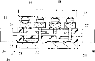
Figure 1A shows the vertical view of the most preferred embodiment of dielectric composite wiring structure of the present invention;
Figure 1B shows the front elevation and the part sectioned view of the most preferred embodiment of the present invention shown in Figure 1A;
Fig. 2 A shows the vertical view of another most preferred embodiment of dielectric composite wiring structure of the present invention;
Fig. 2 B shows the front elevation and the part sectioned view of the most preferred embodiment of the present invention shown in Fig. 2 A;
Fig. 3 A (three-dimensional analysis diagram), 3B and 3C show the details of the assembly method that is used for constituting dielectric composite wiring structure of the present invention;
Fig. 3 D (three-dimensional analysis diagram), 3e and 3F show the further details of the assembly method that is used for constituting dielectric composite wiring structure of the present invention;
Fig. 4 A shows the vertical view of the another embodiment of dielectric composite wiring structure of the present invention;
Fig. 4 B shows along the side cut away view of the embodiment of the invention of IV-IV line among Fig. 4 A; And
Fig. 5 A and 5B show the curved grid componentry in the dielectric medium of being embedded in that adopts dielectric composite wiring structure of the present invention with diagramatic way.
Referring now to Figure 1A, 1B, 2A and 2B, these illustrate the most preferred embodiment that composite construction of the present invention is also referred to as composite wiring structure 10 and 10 ', and Fig. 3 A-3F show be used for making have electric network, the sequential step of the composite construction of the radiator of interconnection and composite dielectric element internal.For easy to understand the present invention, in the whole description below, represent the components identical described in all embodiment with identical reference number.
Though be not limited to this, compound circuit wire structures 10 is main as circuit layout card, or as an alternative, as multi-chip module.In the most preferred embodiment of the present invention shown in Figure 1A and the 1B, composite construction 10 has the hardware 12 that outer first type surface 14 of SIC 16 finally will be installed at least that preferably has on it of a top conductive.The conducting element 18 of any suitable series, electrically contacting between the integrated circuit of composition top metal element 12 and SIC 16.For the most preferred embodiment of the present invention shown in Figure 1A and the 1B, top metal element 12 is as the electrode contact.Composite construction 10 of the present invention also comprises best pottery or organic-ceramic dielectric element 20 and the electrical interconnection network 24 that is bonded to the interior first type surface 22 of top metal element electrode 12 by the covalent bonding method.Electrical interconnection network 24 is embedded in preferably constituting such as the conducting wiring of the metal of copper in pottery or the organic-ceramic component 20 (being also referred to as dielectric element 20) by at least one.One end of copper wiring is at least a position, that is the top metal element electrically contacts the place with SIC 16 formation, is bonded to the interior first type surface 22 of top metal element electrode 12.At least one wiring that forms electrical interconnection network 24 also can have the cloth line terminals 24A that the outside subsurface by dielectric element 20 stretches out alternatively, to form electrically contacting by electrical interconnection network 24 between top metal element electrode 12 and circuit layout card at least one input/output signal driver 25 outward.Describe the another embodiment of the present invention of the installation supporter purposes that explanation interference networks 24 adopt in detail with reference to Fig. 4 A and 4B.Between two top metal element electrodes that metal (preferably copper) wiring that electrically contacting between SIC 16 and the external signal input/output driver also can be formed on by electrical interconnection network 24 is connected.
Fig. 2 A and 2B show another most preferred embodiment of the present invention, and composite wiring structure 10 ' wherein has the top metal element 12 that is divided into electrode district 34 and at least one installing zone 36.In this embodiment of the invention, electrical interconnection network 24 is embedded in the dielectric element 20, and by at least one preferably the conducting wiring of the metal of copper and so on the electrode district 34 of top metal element 12 is connected in the external signal input/output driver.Be bonded to the SIC 16 of the installing zone 36 of top metal element 12, utilize wiring conductor 38, be electrically connected at least one electrode district 34.Electrical interconnection network 24 can be by at least one metal line that stretches out by the subsurface of dielectric element 20, or by another the free electrode district 34 as the part of top metal element 12, SIC 16 is electrically connected to the external signal input/output driver.In addition, in this embodiment of the invention, at least one radiator 28 of heat distribution network 26, the radiator that can stretch out by the subsurface from dielectric element 20 alternatively directly is connected to the installing zone 36 of top metal element 12 fill container 30 (shown in 40) of circuit layout card outside.Bottom metal element 32 is bonded to the outer first type surface of the dielectric element 20 opposite with the first type surface that is bonded to top metal element 12.
Explain the method that makes above-mentioned ceramic composite wiring structure 10 and 10 ' practicability in detail referring now to Fig. 3 A-F.As shown in Figure 3A, preferably thickness is the top metal element 12 of the copper sheet of 0.5-3mm, is used as the substrate of making electrical interconnection network 24, heat distribution network 26 and dielectric element 20 thereon at the beginning.First type surface 14 and interior first type surface 22 specify relative zone as electrode district 34 on the two outside, and if will produce the design shown in the embodiment of Fig. 2 A and 2A, then as installing zone 36.Not all the other zones 42 of specifying zone 44 on the top metal element 12, can use copper sheet or hardware 12 as substrate before optionally cut, corrosion or pressurization, make its thickness less than the appointed area on the first type surface of the top metal element 12 that will become outer first type surface 14.In construction process, preferably outer first type surface 14 is faced down (that is in fact Fig. 3 A-F reverses), and the installation supporter 46 that can move on interior first type surface is placed in those zones in all the other zones 42 that are not used as the circuit layout card part.
Supporter 46 (preferably purgeable) is installed can be made with solid material, this solid material has the end points of the suitable hole of diameter with those sections of the radiator 28 that fixedly is used for forming heat distribution network 26, or even fixedly electric network wiring 24 in some cases.The installation supporter 54 that can remove shown in Fig. 4 A and the 4B can be utilized with the metal line that is used for forming the electrical interconnection network 24 that stretches out from dielectric element 20 subsurfaces.Described the actual detail that supporter 54 is installed in detail with reference to Fig. 4 A and 4B.
As an alternative, purgeable installation supporter 46 can be to solidify after the section of radiator 28 and/or metal line (preferably being made by copper or other Heat Conduction Material) are embedded in wherein or gel changes into the plastic material form of solid or the injection moulding of half cycle body, perhaps can be the form of the combination of solid material and plastic material.If selected material and copper substrate do not form permanent bonding, in 225-475 ℃ technological temperature scope, keep its solid-state or semisolid injection moulding form, but and can the most handyly be stale-proof erosion dielectric element 20, hardware 12 and 32 and the dissolution method of network element 24 and 26 easily remove, then various plastics, glass, pottery or metal material can be used as purgeable installation supporter 46.The injected plastics material of recommending removed comprises the plastic composite that is loaded with sky silicon dioxide and high temperature organic bond that contains polyvinyl formal or polyvinyl butyral resin.Suitable high-temperature adhesives are including, but not limited to the heteroaromatic polymer such as the benzimidazole polymer or be added with a small amount of hydroquinones with the acetenyl termination polyimides of the thermal response that delays acetenyl or the commercially available arylene ether of product Polymer 360 by name or Astrel360.Usually in 350-470 ℃ temperature range, make purgeable injected plastics material down in the pressure of 50-2000psi, and should be made into can bear ceramic processing temperature (225-475 ℃), can resist the corrosive agent of the remaining area 42 that is used for removing hardware 12 and 32, also will be for to dielectric element 20, hardware 12 and 32 and comprise dispersion sensitivity in the inactive solvent of material of electrical interconnection network 24 and heat dissipation network 26.
Also comprise part and do not constitute the fill container that the material removed 48 of final circuit board component and radiator 28 that heat distribution network 26 stretches out by the subsurface from dielectric element 20 that is embedded in the dielectric element 20 connect thereon if some installs supporter 46, then can improve manufacturing efficient.Radiator/installation supporter is merely able to be arranged in all the other zones 42 contiguous with the subsurface of dielectric element 20, and the radiator 28 that only is connected in the heat distribution network stretches out by this subsurface.
In case finished circuit layout card, the section of the radiator 28 that those that are used for making those copper wiring sections 50 of electrical interconnection network 24 and are used for making heat distribution network 26 stretch out from dielectric element 20 just is embedded in and installs in the supporter 46.When fill container 30 was combined as the parts that supporter 46 is installed, those radiator sections that stretch out from dielectric element 20 subsurfaces by the material 48 of supporter is installed, were fixed to fill container 30.Then, shown in Fig. 3 B, have connect up those of all the other zones 42 on the installation supporter 46 of embedding section and the inner surface 22 that radiator is placed in top metal element 12 of copper and need not do on the zone of compound wiring plate part.
Then, shown in Fig. 3 B, form the end points of the metal line of electrical interconnection network 24, be bonded to inner surface 22 as the sheet metal at described those area places that are defined as electrode district 34 of Fig. 2 A.Can metal line be bonded to sheet metal with various brazing materials known to those skilled in the art, electric welding, arc welding or ultrasonic bonding.The bonding techniques of the electric property that the circuit layout card that selection is suitable for finishing is desired is recommendable.Though also can be with other routine techniques, the best approach of the present invention is to adopt bonding techniques such as arc welding to form metal bonding between the regulation electrode district 34 of electrical interconnection network 24 and copper sheet metal.
Electrically contact to another metal line or a plurality of such metal line by means of the metal line of crooked bonding and with it, make electrical interconnection network 24, thereby constitute in the mode consistent with SIC and the distinctive wiring figure of outside input/output signal driver.Though arc welding is to make the recommend method of the electrical interconnection between metal (preferably copper) wiring that constitutes like this, also can adopt other conventional method.By means of the copper wiring and any other copper wire bond selecting will not constitute like this, and in another electrode district termination sealing via metal wiring, or by means of the via metal wiring that stops sealing in purgeable installation supporter, the present invention can be used to make the through hole of sealing.With for example vacuum pressing and casting method, also can be produced on its end points place and be press fitted into the prefabricated routing network that is used for making electrical interconnection network 24 in the insert 52 in the electrode district 34 that pierces the copper sheet substrate.For simplicity, Fig. 3 B shows this method for preparing the electrical interconnection network.According to Fig. 2 A and the described most preferred embodiment of b, in the time will producing the circuit layout card that comprises electrode district and installing zone, can touch the method for electrode district 34 with the above-mentioned end points that is used for making electrical interconnection network 24, the contact zone that will comprise the radiator 28 of heat distribution network 26 is bonded to installing zone 36.
As mentioned above, after circuit layout card " CWB " is assembled fully, can remove alternatively supporter 46 is installed.Also the installation supporter can be retained among the finished product CWB as an element, as a permanent fixture.Shown in Fig. 4 A and 4B, conducting wiring 50 that supporter 54 will form electrical interconnection network 24 is installed is electrically connected to input/output signal driver (not shown) outside the CWB.Fig. 4 A and 4B show the complete form that comprises the present embodiment that is electrically connected permanent installation supporter.
In case electrical interconnection network 24 and heat distribution network 26 are fixed to metal substrate shown in Fig. 3 B, with regard to the method for closing with the direct covalent bonds that forms between hardware and pottery or the organic-Ceramic Composite dielectric medium, by means of solution process, the dielectric material 20A that will form dielectric element 20 shown in Fig. 3 C is coated to metal substrate and network configuration.Can use the technology such as sol-gel and/or metal organic decomposition (" MOD "), ceramic precursor is dissolved in the solution.Above-mentioned sol-gel technique utilizes the metal alkoxide precursor, concentrates reaction by alcohol and comes the polymer-inorganic ceramic network.By means of with precursor batching cast, spraying, spraying-pyrolysis or be screen-printed to, the precursor solution of suitable thickness can be coated to metal substrate and network configuration by in the purgeable installation supporter 46 determined traps.Then by means of the organic precursor of metal is heated to its temperature more than decomposition point (that is, preferably 225-475 ℃), perhaps, under the situation of the pottery that MOD prepares, by means of heating evaporation from the pottery that sol-gel generates with acceleration polymerization and alcohol, precursor is reacted in oxidizing atmosphere promptly decompose, thereby form needed ceramic phase.
Relative dielectric constant is that 10 aluminium oxide and relative dielectric constant are 3.8 silicon dioxide, owing under the situation of pure silicon dioxide ceramic component, can limit dielectric loss, thereby the signal of telecommunication can be propagated by electrical interconnection network 24 with the frequency up to 1.2-1.5GHz, and become best ceramic phase.
Can be with the solution of continuous reduction viscosity prepare burden again coated with ceramic precursor and reaction repeated/decomposition, to be filled in the cavity that makes at the beginning among dielectric medium (pottery) 20A that may exist after the ceramic component.By means of using low dielectric such as polyvinyl formal or the organic batching infiltration that eliminates stress or soaking into ceramic component, organic to form-the Ceramic Composite dielectric medium, also can fill this cavity.The dielectric constant of polyvinyl formal is 3, and loss factor is 0.02, and dielectric strength (1/8 thickness) equals 300V/mm.Dielectric constant is 2.6 and loss factor be 0.027 polyvinyl butyral resin is another bleeding agent that is fit to.The employing of carboxylate precursor and MOD technology is a most preferred embodiment of the present invention.For the aluminium oxide ceramics element, 2 ethyl hexanoic acid aluminium (alumina 2-ethylhexanoate) is the best organic precursor of metal, and for the SiO 2-ceramic element, 2 ethyl hexanoic acid silicon is the best organic precursor of metal.
Also can with the solution spraying pyrolysis at the initial decomposition temperature (225-375 ℃) of the carboxylate that is heated to above dissolving and be lower than method on the circuit layout card assembly parts of the complete decomposition temperature of organic ligand (400-475 ℃) of salt, make organic-Ceramic Composite dielectric material.In spraying-pyrolytic process, carboxylic acid evaporation, the wax shape carboxylate of decomposition in situ under the deposit.When the circuit layout card assembly parts were heated to appropriate temperature, the dielectric material that obtains was the oxide ceramics matrix of complete deflagration with organic material of incomplete decomposing, thereby produces organic-ceramic dielectric element.If the dielectric medium and the wiring assembly parts of deposit are not exposed to the temperature more than 400 ℃ that organic component is decomposed sharp, then can keep this organic-ceramic composite.By means of low volatility resin that will be such as polyvinyl butyral resin, and/or the high-temperature adhesives consistent with polyvinyl butyral resin, add in carboxylate (" the MOD ") solution, can improve the organic content in the organic-Ceramic Composite dielectric medium of these spraying-pyrolysis.Polyvinyl butyral resin decomposes under the temperature more than 450 ℃ usually, and is attached on the carboxylate matrix of decomposing by the part of deposit under the 225-375 ℃ of temperature.
In case shown in Fig. 3 E, made whole compound, just by means of to those attenuates of top metal element 12 and bottom metal element 32 part corrode, remove all the other zones 42 that do not constitute finished product wiring plate portion.Pulverized respectively in case the compound that part is finished must design and be configured to all the other zones of top metal element 12 and bottom metal element 32, just exposed the material removed 48 that supporter 46 is installed.Pulverize the material the removed part 48 that supporter 46 is installed then, to obtain the finished product compound circuit wiring plate shown in Fig. 3 E with internal copper wiring electrical interconnection and heat distribution network.
In yet another embodiment of the present invention, at least one inner blocking capacitor, preferably solid-state is ceramic capacitor (being appointed as capacitor 60A and 60B separately), and at least one conducting wiring 50 in the electrical interconnection network 24 is connected in earth potential.Select the electric capacity of inner blocking capacitor 60A and B, so that reduce the signal to noise ratio that any unwanted parasitic signal of telecommunication (noise) also improves the signal of telecommunication of advancing by the electrical interconnection network 24 between any input/output signal driver (not shown) of SIC and CWB outside.Fig. 4 B shows the access of inner blocking capacitor, is equipped with the hardware 32 of SIC on wherein relative with hardware 12 its, has been configured to the earth potential effect.
Before will wrapping up that part of dielectric element 20 of inner blocking capacitor 60A in coating, inner blocking capacitor 60A is fixed on the hardware 32, inner blocking capacitor 60A can be embedded in the dielectric element 20.By means of making through holes 62 at the dielectric substance 20 that is arranged in above the inner blocking capacitor 60A, and use conductive materials 64 filling vias 62 that also electrically contact with at least one conducting wiring 50 such as scolder or metal-to-metal adhesive, capacitor 60A can be electrically connected at least one conducting wiring 50 in the electrical interconnection network 24.
Utilize the present invention, inner blocking capacitor 60B might be placed in a permanent fixture that is retained as CWB in the supporter 54 is installed.As capacitor 60A, the through hole 62 with conductive materials 64 also electrically contacts with at least one conducting wiring 50.Capacitor 60B is used to SIC is electrically connected to by electrical interconnection network 24 the input/output signal driver of CWB outside.In Fig. 4 B, also show this most preferred embodiment of the present invention.The example that can be used in blocking capacitor of the present invention can be but be not limited to ceramic capacitor, preferably multilayer ceramic capacitor.
The internal stress that takes place when the root problem of combination metal line or piping network relates to the huge mismatch of thermal coefficient of expansion between metal and the ceramic dielectric matter component and compound thermal cycle in dielectric element, break or deformation.When thermal coefficient of expansion is 16.5 * 10
-6/ ℃ copper to be embedded in thermal coefficient of expansion be 0.5 * 10
-6/ ℃ pure silicon dioxide in the time, this problem especially severe.At thermal coefficient of expansion is 8.8 * 10
-6/ ℃ aluminium oxide ceramics and the mismatch between the copper not seriously like this, problem is less.The heat that SIC 16 produces is dissipated in the circuit layout card.When heat distribution network 26 is sent to the radiator of circuit layout card outside with this heat, can makes the dielectric element heating, expand and compression.
Used two kinds of methods to alleviate the adverse effect of stress in the present invention to ceramic component and embedding network configuration.The firstth, the curve in the embedding network configuration design is placed the high stress point of sharp edge along the structure initiation.Be connected with the pointed shape L shown in the 5B when being connected with T when network configuration is designed to curve rather than Fig. 5 A, stress more is evenly distributed on the circular arc, and can not set up strong pressure at the sharp point place of network.The optimal curvatures radius that network connects, even be used for forming the copper wiring of these networks or the concrete cross sectional shape of radiator, depend on the heat load that SIC applies, and can derive out by any skilled person such as the computer simulation method technical field of Finite Element Method.Second, by means of as shown in Figure 3A, use the sector of breakdown that is higher than 430 ℃ polyvinyl formal such as decomposition temperature comprise high-temperature adhesives organic resin 56 coatings formation electrical interconnection networks 24 (copper) metal line and form the hot channel 28 of heat dissipation network 26, also reduced compression.Can be used in prefabricated network and be fixed to before top metal element 12 and/or the installation supporter 46,, come application of resin the method in its immersion resin bath.In the present invention, preferably use " pultrusion " method to apply organic resin, thereby in the electrical interconnection network 24 on being assembled to the sheet metal substrate surface time, the metal line element is pulled through the applicator die of application of resin.The high decomposition temperature of resin makes resin can occupy the next-door neighbour space of network element.Under the temperature that is lower than the resin decomposition, the surface of organic resin is made and hardened to ceramic component.The organic resin of " soft " can stay as the resilient coating that adapts to the inhomogeneous lateral displacement between metalolic network element and the ceramic component.
The resin compound of coating then must resist to be used for pulverizing the solvent that the material removed 48 in the supporter 46 is installed if will be left the part of compound.As an alternative, by means of in oxidizing atmosphere, compound being heated to above its heat decomposition temperature, or, also can remove resin by means of it being dissolved in the suitable dispersant.In case resin is eliminated, between the ceramic component that hardens and metal line and/or radiator, just produce void space.This void space makes network element when the metalolic network element expands or shrink greatlyyer than dielectric element on every side, can be with respect to dielectric element slippage on every side.The degree of depth of void space, thereby also be the thickness of organic resin coating depends on metalolic network element in the high duty cycle process of given SIC and the relativity degree that may need between the dielectric medium on every side.
Though described the present invention for various embodiment, should be understood that, in the design and scope of claims, the present invention also can have various further and other embodiment.
Claims (29)
1. the ceramic substrate of composite wiring structure is arranged, and it comprises:
At least one forms the electric conductor of an electric network part and the heat carrier of at least one formation heat supply network network part, described electric conductor is bonded to described ceramic substrate in described ceramic substrate, described ceramic substrate is as electrical insulator, and described ceramic substrate surrounds electric network and heat supply network network;
Thereby formed described electric conductor and heat carrier and electric network and heat supply network network are arranged in the described ceramic substrate, and be electrically isolated from one; And
The described composite wiring structure of described ceramic substrate is configured and is arranged to and heat can be sent to and transmit by the heat supply network network from electric network and semiconductor device.
2. the described ceramic substrate of claim 1 is by means of making around the pottery of described electric network and described heat supply network network and make described ceramic substrate being not enough to original position under the temperature that structural intergrity to described electric network and described heat supply network network causes adverse effect.
3. the described ceramic substrate of claim 2, wherein said ceramic substrate is by being bonded to described at least one electric conductor being lower than 475 ℃ of covalent bondings that form down.
4. the described ceramic substrate of claim 2, wherein said ceramic substrate is by being lower than the network that 475 ℃ of covalent bondings that form down are bonded to described at least one electric conductor and heat carrier and form like this.
5. the described ceramic substrate of claim 3, wherein said electric network and heat supply network network are made of the element that is coated with being higher than 475 ℃ of organic resins that decompose down.
6. the described ceramic substrate of claim 1, wherein said electric network is made of the conducting wiring section of a plurality of interconnection, and the described wiring section of part stretches out by the first type surface of described ceramic substrate, so that be electrically connected at least one semiconductor device.
7. the described ceramic substrate of claim 1, the described heat supply network network that is connected to that also comprises described ceramic substrate outside is used for providing for described heat distribution network the device of fill container.
8. the described ceramic substrate of claim 1 also comprises and is used for described electric network is electrically connected to the extra conducting element of at least one semiconductor device.
9. the described ceramic substrate of claim 1, also comprise at least one be embedded in the described ceramic substrate and be connected electrically in described electric network and another electric conductor between capacitor.
10. the described ceramic substrate of claim 1, wherein said electric network and heat supply network network are made of the curve element.
11. the described ceramic substrate of claim 1 also comprises supporting structure, and described electric network and heat supply network network are fixed to described supporting structure.
12. the described ceramic substrate of claim 11, wherein said supporting structure comprises the fill container that is used for described heat supply network network.
13. the described ceramic substrate of claim 1, wherein said heat supply network network is made of at least one radiator, and the described radiator of part can be connected to described at least one electric conductor.
14. the described ceramic substrate of claim 1, wherein at least one semiconductor device and described at least one electric conductor combination.
15. the described ceramic substrate of claim 1, wherein at least one semiconductor device and described at least one electric conductor and heat carrier combination.
16. the described ceramic substrate of claim 1, wherein said ceramic substrate are organic-potteries.
17. the described ceramic substrate of claim 1, wherein said ceramic substrate comprises the Al-base ceramic material.
18. the described ceramic substrate of claim 1, wherein said ceramic substrate comprises the silicon dioxide base ceramic material.
19. a building method that is used in the composite construction at least one semiconductor device, it comprises the following step:
Provide at least one electric conductor to form the part electric network;
Provide at least one heat carrier to form the portion of hot network; And
Close by means of form direct covalent bonds between described electric conductor and described dielectric material, dielectric material is coated to described electric conductor, described heat supply network network and described electric network are surrounded by described dielectric material.
20. the building method of the described composite construction of claim 19, the step that also is included in the described dielectric material of coating provides the step of the capacitor at least one described dielectric material before, and described at least one capacitor is connected electrically between described electric network and the conducting element.
21. the building method of the described composite construction of claim 19 also comprises to provide and has at least one conducting wiring section and make described electric network and the step of described heat supply network network electric insulation.
22. the building method of the described composite construction of claim 19 also is included in the described dielectric material of coating and before described heat supply network network is fixed to the step of installing on the supporter.
23. the building method of the described composite construction of claim 19 also comprises the part first type surface of optionally removing described electric conductor and is used for installing the step of the electrode district of semiconductor device thereon to determine at least one.
24. the building method of the described composite construction of claim 19, wherein said dielectric material comprises Al-base ceramic.
25. the building method of the described composite construction of claim 19, wherein said dielectric material comprises organic-pottery.
26. the building method of the described composite construction of claim 19 also comprises by means of spray pyrolysis and contains the solution of carboxylic acid precursor of polyvinyl butyral resin and the step of making composite construction.
27. the building method of the described composite construction of claim 19, wherein said dielectric material comprises the silicon-dioxide-substrate pottery.
28. the building method of the described composite construction of claim 19 also comprises the step that at least one semiconductor device is electrically connected to described electric conductor.
29. the building method of the described composite construction of claim 19 also comprises at least one semiconductor device is connected to described electric conductor and described heat carrier.
Applications Claiming Priority (2)
| Application Number | Priority Date | Filing Date | Title |
|---|---|---|---|
| US3398396P | 1996-12-30 | 1996-12-30 | |
| US60/033,983 | 1996-12-30 |
Publications (2)
| Publication Number | Publication Date |
|---|---|
| CN1245629A CN1245629A (en) | 2000-02-23 |
| CN1112838C true CN1112838C (en) | 2003-06-25 |
Family
ID=21873603
Family Applications (1)
| Application Number | Title | Priority Date | Filing Date |
|---|---|---|---|
| CN97181620A Expired - Fee Related CN1112838C (en) | 1996-12-30 | 1997-12-29 | Ceramic composite wiring structure for semiconductor devices and method of manufacture thereof |
Country Status (5)
| Country | Link |
|---|---|
| EP (1) | EP0948879A4 (en) |
| JP (1) | JP2001507867A (en) |
| CN (1) | CN1112838C (en) |
| CA (1) | CA2275972A1 (en) |
| WO (1) | WO1998030072A1 (en) |
Cited By (1)
| Publication number | Priority date | Publication date | Assignee | Title |
|---|---|---|---|---|
| CN102210844B (en) * | 2010-04-07 | 2012-10-31 | 北京亚东生物制药有限公司 | Chinese medicinal composition for treating chronic hepatitis and preparation method thereof |
Families Citing this family (6)
| Publication number | Priority date | Publication date | Assignee | Title |
|---|---|---|---|---|
| US6346743B1 (en) * | 2000-06-30 | 2002-02-12 | Intel Corp. | Embedded capacitor assembly in a package |
| DE10232788B4 (en) * | 2001-07-18 | 2010-01-14 | Infineon Technologies Ag | Electronic component with a semiconductor chip on a system carrier, system carrier and method for producing an electronic component |
| DE102008001414A1 (en) * | 2008-04-28 | 2009-10-29 | Robert Bosch Gmbh | Substrate circuit module with components in multiple contacting levels |
| CN102314526B (en) * | 2010-07-02 | 2013-09-25 | 中国科学院微电子研究所 | Method for optimizing integrated circuit layout heat distribution |
| JP5488540B2 (en) * | 2011-07-04 | 2014-05-14 | トヨタ自動車株式会社 | Semiconductor module |
| CN111328189A (en) * | 2020-03-17 | 2020-06-23 | 万安裕维电子有限公司 | Salt mist resistant PCB |
Family Cites Families (10)
| Publication number | Priority date | Publication date | Assignee | Title |
|---|---|---|---|---|
| US3676292A (en) * | 1970-10-07 | 1972-07-11 | Olin Corp | Composites of glass-ceramic-to-metal,seals and method of making same |
| JPS6028296A (en) * | 1983-07-27 | 1985-02-13 | 株式会社日立製作所 | Ceramic multilayer printed circuit board |
| JPH02501179A (en) * | 1988-02-29 | 1990-04-19 | ディジタル イクイプメント コーポレーション | System for aligning leads in ceramic integrated circuit packages |
| US5336532A (en) * | 1989-02-21 | 1994-08-09 | Dow Corning Corporation | Low temperature process for the formation of ceramic coatings |
| US5113315A (en) * | 1990-08-07 | 1992-05-12 | Cirqon Technologies Corporation | Heat-conductive metal ceramic composite material panel system for improved heat dissipation |
| JP3026465B2 (en) * | 1992-03-10 | 2000-03-27 | 株式会社日立製作所 | Ceramic thin film hybrid wiring board and manufacturing method |
| US5506755A (en) * | 1992-03-11 | 1996-04-09 | Kabushiki Kaisha Toshiba | Multi-layer substrate |
| DE4222474A1 (en) * | 1992-07-09 | 1994-01-13 | Bosch Gmbh Robert | Assembly unit for multi-layer hybrid with power components |
| US5444298A (en) * | 1993-02-04 | 1995-08-22 | Intel Corporation | Voltage converting integrated circuit package |
| JPH06255019A (en) * | 1993-03-08 | 1994-09-13 | Hitachi Ltd | Ceramic composite laminated sheet and production of multilayer wiring board used therewith |
-
1997
- 1997-12-29 EP EP97954258A patent/EP0948879A4/en not_active Withdrawn
- 1997-12-29 CN CN97181620A patent/CN1112838C/en not_active Expired - Fee Related
- 1997-12-29 JP JP53025098A patent/JP2001507867A/en not_active Ceased
- 1997-12-29 WO PCT/US1997/023976 patent/WO1998030072A1/en active Application Filing
- 1997-12-29 CA CA002275972A patent/CA2275972A1/en not_active Abandoned
Cited By (1)
| Publication number | Priority date | Publication date | Assignee | Title |
|---|---|---|---|---|
| CN102210844B (en) * | 2010-04-07 | 2012-10-31 | 北京亚东生物制药有限公司 | Chinese medicinal composition for treating chronic hepatitis and preparation method thereof |
Also Published As
| Publication number | Publication date |
|---|---|
| WO1998030072A1 (en) | 1998-07-09 |
| CN1245629A (en) | 2000-02-23 |
| EP0948879A1 (en) | 1999-10-13 |
| JP2001507867A (en) | 2001-06-12 |
| CA2275972A1 (en) | 1998-07-09 |
| EP0948879A4 (en) | 2003-08-27 |
Similar Documents
| Publication | Publication Date | Title |
|---|---|---|
| US6323549B1 (en) | Ceramic composite wiring structures for semiconductor devices and method of manufacture | |
| CN1065660C (en) | Substrate for semiconductor package, fabrication method thereof, and stacked type semiconductor package using substrate | |
| CN1203731C (en) | Method for producing multilayer cicuit board and multilayer circuitboard produced by said method | |
| CN104517909B (en) | Semiconductor module and its manufacture method with printed circuit board | |
| CN1266764C (en) | Semiconductor device and its producing method | |
| CN1247053C (en) | Multilayer circuit board and method for manufacturing multilayer circuit board | |
| DE10336171B3 (en) | Multi-chip circuit module and method of making this | |
| DE102018116847A1 (en) | Ceramic module for power semiconductor integrated packaging and its preparation method | |
| CN1691871A (en) | Multilayer substrate including components therein | |
| CN110517991B (en) | Metal ceramic module and manufacturing method thereof, circuit board module and manufacturing method thereof | |
| CN1157773C (en) | Metal core substrate printed wiring board enabling thermally enhanced ball grid array (BGA) packages and method | |
| CN1946271A (en) | Printed circuit board and manufacturing method thereof | |
| CN1971863A (en) | Semiconductor chip buried base plate 3D construction and its manufacturing method | |
| JPH0563106B2 (en) | ||
| CN1112838C (en) | Ceramic composite wiring structure for semiconductor devices and method of manufacture thereof | |
| CN1832659A (en) | Circuit device and method of manufacturing thereof | |
| CN1767178A (en) | Semiconductor substrate and manufacturing method thereof and semiconductor package assembly | |
| CN1797726A (en) | Semiconductor structured chip embedded structure of base plate and method of preparation | |
| WO1998030072A9 (en) | Ceramic composite wiring structures for semiconductor devices and method of manufacture | |
| US20020048927A1 (en) | Embedded capacitor multi-chip modules | |
| EP2219211A1 (en) | Substrate for holding at least one component and method for producing a substrate | |
| CN212570968U (en) | Heat dissipation embedding packaging structure | |
| CN1835211A (en) | Circuit board of electronic device and mfg method thereof | |
| CN1638104A (en) | Hybrid integrated circuit device and manufacturing method of the same | |
| JPH1117348A (en) | Wiring board and manufacture thereof |
Legal Events
| Date | Code | Title | Description |
|---|---|---|---|
| C06 | Publication | ||
| PB01 | Publication | ||
| C10 | Entry into substantive examination | ||
| SE01 | Entry into force of request for substantive examination | ||
| C14 | Grant of patent or utility model | ||
| GR01 | Patent grant | ||
| C17 | Cessation of patent right | ||
| CF01 | Termination of patent right due to non-payment of annual fee |
Granted publication date: 20030625 Termination date: 20101229 |