CN111063787A - Light emitting device with self-aligned preformed lens - Google Patents
Light emitting device with self-aligned preformed lens Download PDFInfo
- Publication number
- CN111063787A CN111063787A CN201911355103.9A CN201911355103A CN111063787A CN 111063787 A CN111063787 A CN 111063787A CN 201911355103 A CN201911355103 A CN 201911355103A CN 111063787 A CN111063787 A CN 111063787A
- Authority
- CN
- China
- Prior art keywords
- light emitting
- cavity
- lens structure
- lens
- emitting device
- Prior art date
- Legal status (The legal status is an assumption and is not a legal conclusion. Google has not performed a legal analysis and makes no representation as to the accuracy of the status listed.)
- Pending
Links
- 238000000034 method Methods 0.000 claims description 28
- 239000000463 material Substances 0.000 claims description 19
- 229920001296 polysiloxane Polymers 0.000 claims description 18
- 230000003287 optical effect Effects 0.000 claims description 17
- 150000001875 compounds Chemical group 0.000 claims description 3
- 239000011521 glass Substances 0.000 claims description 3
- 238000006073 displacement reaction Methods 0.000 claims 1
- 239000000758 substrate Substances 0.000 abstract description 28
- 238000003780 insertion Methods 0.000 abstract description 21
- 230000037431 insertion Effects 0.000 abstract description 20
- 239000000853 adhesive Substances 0.000 abstract description 15
- 230000001070 adhesive effect Effects 0.000 abstract description 15
- 238000004519 manufacturing process Methods 0.000 abstract description 6
- 230000008569 process Effects 0.000 description 15
- 239000000919 ceramic Substances 0.000 description 5
- 238000005520 cutting process Methods 0.000 description 4
- 239000010410 layer Substances 0.000 description 4
- 238000000465 moulding Methods 0.000 description 4
- 238000004806 packaging method and process Methods 0.000 description 4
- 230000008878 coupling Effects 0.000 description 3
- 238000010168 coupling process Methods 0.000 description 3
- 238000005859 coupling reaction Methods 0.000 description 3
- 239000004593 Epoxy Substances 0.000 description 2
- 239000004020 conductor Substances 0.000 description 2
- 238000005553 drilling Methods 0.000 description 2
- 239000002184 metal Substances 0.000 description 2
- 239000000203 mixture Substances 0.000 description 2
- 230000001681 protective effect Effects 0.000 description 2
- 238000007493 shaping process Methods 0.000 description 2
- 238000004513 sizing Methods 0.000 description 2
- 239000010409 thin film Substances 0.000 description 2
- 239000012790 adhesive layer Substances 0.000 description 1
- 239000011324 bead Substances 0.000 description 1
- 230000008901 benefit Effects 0.000 description 1
- 239000003990 capacitor Substances 0.000 description 1
- 238000006243 chemical reaction Methods 0.000 description 1
- 230000002950 deficient Effects 0.000 description 1
- 230000001419 dependent effect Effects 0.000 description 1
- 230000009977 dual effect Effects 0.000 description 1
- 230000000694 effects Effects 0.000 description 1
- 238000005538 encapsulation Methods 0.000 description 1
- 238000005516 engineering process Methods 0.000 description 1
- 238000009472 formulation Methods 0.000 description 1
- 238000005286 illumination Methods 0.000 description 1
- 238000011031 large-scale manufacturing process Methods 0.000 description 1
- 239000007788 liquid Substances 0.000 description 1
- 238000012858 packaging process Methods 0.000 description 1
- 230000007704 transition Effects 0.000 description 1
Images


Classifications
-
- G—PHYSICS
- G02—OPTICS
- G02B—OPTICAL ELEMENTS, SYSTEMS OR APPARATUS
- G02B3/00—Simple or compound lenses
- G02B3/0006—Arrays
- G02B3/0075—Arrays characterized by non-optical structures, e.g. having integrated holding or alignment means
-
- F—MECHANICAL ENGINEERING; LIGHTING; HEATING; WEAPONS; BLASTING
- F21—LIGHTING
- F21V—FUNCTIONAL FEATURES OR DETAILS OF LIGHTING DEVICES OR SYSTEMS THEREOF; STRUCTURAL COMBINATIONS OF LIGHTING DEVICES WITH OTHER ARTICLES, NOT OTHERWISE PROVIDED FOR
- F21V17/00—Fastening of component parts of lighting devices, e.g. shades, globes, refractors, reflectors, filters, screens, grids or protective cages
- F21V17/10—Fastening of component parts of lighting devices, e.g. shades, globes, refractors, reflectors, filters, screens, grids or protective cages characterised by specific fastening means or way of fastening
- F21V17/101—Fastening of component parts of lighting devices, e.g. shades, globes, refractors, reflectors, filters, screens, grids or protective cages characterised by specific fastening means or way of fastening permanently, e.g. welding, gluing or riveting
-
- F—MECHANICAL ENGINEERING; LIGHTING; HEATING; WEAPONS; BLASTING
- F21—LIGHTING
- F21V—FUNCTIONAL FEATURES OR DETAILS OF LIGHTING DEVICES OR SYSTEMS THEREOF; STRUCTURAL COMBINATIONS OF LIGHTING DEVICES WITH OTHER ARTICLES, NOT OTHERWISE PROVIDED FOR
- F21V19/00—Fastening of light sources or lamp holders
- F21V19/001—Fastening of light sources or lamp holders the light sources being semiconductors devices, e.g. LEDs
- F21V19/0015—Fastening arrangements intended to retain light sources
- F21V19/002—Fastening arrangements intended to retain light sources the fastening means engaging the encapsulation or the packaging of the semiconductor device
-
- F—MECHANICAL ENGINEERING; LIGHTING; HEATING; WEAPONS; BLASTING
- F21—LIGHTING
- F21V—FUNCTIONAL FEATURES OR DETAILS OF LIGHTING DEVICES OR SYSTEMS THEREOF; STRUCTURAL COMBINATIONS OF LIGHTING DEVICES WITH OTHER ARTICLES, NOT OTHERWISE PROVIDED FOR
- F21V5/00—Refractors for light sources
- F21V5/007—Array of lenses or refractors for a cluster of light sources, e.g. for arrangement of multiple light sources in one plane
-
- G—PHYSICS
- G02—OPTICS
- G02B—OPTICAL ELEMENTS, SYSTEMS OR APPARATUS
- G02B19/00—Condensers, e.g. light collectors or similar non-imaging optics
- G02B19/0033—Condensers, e.g. light collectors or similar non-imaging optics characterised by the use
- G02B19/0047—Condensers, e.g. light collectors or similar non-imaging optics characterised by the use for use with a light source
- G02B19/0061—Condensers, e.g. light collectors or similar non-imaging optics characterised by the use for use with a light source the light source comprising a LED
- G02B19/0066—Condensers, e.g. light collectors or similar non-imaging optics characterised by the use for use with a light source the light source comprising a LED in the form of an LED array
-
- G—PHYSICS
- G02—OPTICS
- G02B—OPTICAL ELEMENTS, SYSTEMS OR APPARATUS
- G02B3/00—Simple or compound lenses
- G02B3/0006—Arrays
- G02B3/0037—Arrays characterized by the distribution or form of lenses
- G02B3/0056—Arrays characterized by the distribution or form of lenses arranged along two different directions in a plane, e.g. honeycomb arrangement of lenses
-
- H—ELECTRICITY
- H01—ELECTRIC ELEMENTS
- H01L—SEMICONDUCTOR DEVICES NOT COVERED BY CLASS H10
- H01L25/00—Assemblies consisting of a plurality of individual semiconductor or other solid state devices ; Multistep manufacturing processes thereof
- H01L25/03—Assemblies consisting of a plurality of individual semiconductor or other solid state devices ; Multistep manufacturing processes thereof all the devices being of a type provided for in the same subgroup of groups H01L27/00 - H01L33/00, or in a single subclass of H10K, H10N, e.g. assemblies of rectifier diodes
- H01L25/04—Assemblies consisting of a plurality of individual semiconductor or other solid state devices ; Multistep manufacturing processes thereof all the devices being of a type provided for in the same subgroup of groups H01L27/00 - H01L33/00, or in a single subclass of H10K, H10N, e.g. assemblies of rectifier diodes the devices not having separate containers
- H01L25/075—Assemblies consisting of a plurality of individual semiconductor or other solid state devices ; Multistep manufacturing processes thereof all the devices being of a type provided for in the same subgroup of groups H01L27/00 - H01L33/00, or in a single subclass of H10K, H10N, e.g. assemblies of rectifier diodes the devices not having separate containers the devices being of a type provided for in group H01L33/00
- H01L25/0753—Assemblies consisting of a plurality of individual semiconductor or other solid state devices ; Multistep manufacturing processes thereof all the devices being of a type provided for in the same subgroup of groups H01L27/00 - H01L33/00, or in a single subclass of H10K, H10N, e.g. assemblies of rectifier diodes the devices not having separate containers the devices being of a type provided for in group H01L33/00 the devices being arranged next to each other
-
- H—ELECTRICITY
- H01—ELECTRIC ELEMENTS
- H01L—SEMICONDUCTOR DEVICES NOT COVERED BY CLASS H10
- H01L33/00—Semiconductor devices with at least one potential-jump barrier or surface barrier specially adapted for light emission; Processes or apparatus specially adapted for the manufacture or treatment thereof or of parts thereof; Details thereof
- H01L33/48—Semiconductor devices with at least one potential-jump barrier or surface barrier specially adapted for light emission; Processes or apparatus specially adapted for the manufacture or treatment thereof or of parts thereof; Details thereof characterised by the semiconductor body packages
- H01L33/58—Optical field-shaping elements
- H01L33/60—Reflective elements
-
- H—ELECTRICITY
- H01—ELECTRIC ELEMENTS
- H01L—SEMICONDUCTOR DEVICES NOT COVERED BY CLASS H10
- H01L33/00—Semiconductor devices with at least one potential-jump barrier or surface barrier specially adapted for light emission; Processes or apparatus specially adapted for the manufacture or treatment thereof or of parts thereof; Details thereof
- H01L33/48—Semiconductor devices with at least one potential-jump barrier or surface barrier specially adapted for light emission; Processes or apparatus specially adapted for the manufacture or treatment thereof or of parts thereof; Details thereof characterised by the semiconductor body packages
- H01L33/62—Arrangements for conducting electric current to or from the semiconductor body, e.g. lead-frames, wire-bonds or solder balls
-
- H—ELECTRICITY
- H01—ELECTRIC ELEMENTS
- H01L—SEMICONDUCTOR DEVICES NOT COVERED BY CLASS H10
- H01L2933/00—Details relating to devices covered by the group H01L33/00 but not provided for in its subgroups
- H01L2933/0008—Processes
- H01L2933/0033—Processes relating to semiconductor body packages
- H01L2933/0058—Processes relating to semiconductor body packages relating to optical field-shaping elements
Abstract
A lens structure is preformed with features that facilitate precise alignment of light emitting chips within the lens structure. To facilitate manufacturing, the features include tapered walls that allow easy insertion of the light emitting chip into the lens structure, the taper serving to precisely align the light emitting chip when the chip is fully inserted. The cone may comprise linearly inclined or curved walls, which comprise complex shapes. An adhesive may be used to secure the light emitting chip to the lens structure. The light emitting chips may be picked and placed into an array of lens structures or onto a substrate that may be covered by an array of lens structures.
Description
Technical Field
The present invention relates to the field of light emitting devices, and in particular to light emitting devices formed by placing a self-supporting light emitting element into a preformed lens having a cavity with inclined walls that facilitate insertion of the light emitting element into the lens and adhesion of the light emitting element to the lens.
Background
Conventional light emitting devices include a light emitting element, such as a light emitting diode chip (LED chip) mounted on a substrate and enclosed in a protective enclosure that can act as an optical lens. The substrate provides the structural support required to facilitate handling of the light emitting device during subsequent processes, such as mounting of the light emitting device on a printed circuit board. The protective housing may include a wavelength conversion material that converts at least a portion of the light emitted from the light emitting chip to light of a different wavelength. The wavelength converting material may alternatively be provided as a discrete element between the light emitting chip and the housing/lens.
A common technique for providing a light emitting apparatus as described above includes attaching a light emitting element to a leadframe substrate for allowing external power connection to the light emitting element, and then encapsulating the light emitting element and a portion of the leadframe to which it is attached with a silicone mold. The wire frame may be part of a carrier comprising a plurality of frames for mounting the light emitting elements, such that the encapsulation may be performed for all light emitting elements as a single molding process.
In another embodiment, the light emitting element is mounted on a ceramic substrate that includes conductors to which the light emitting element is attached. USP 7,452,737, "MOLDED LENS OVER LED DIE", issued 11/18.2008 to grisory base, Robert Scott West and Paul s. The ceramic substrate may then be cut/diced to provide a "singulated" light emitting device, which includes external connections to the light emitting elements on the ceramic substrate.
In another embodiment, the substrate comprises a cup-shaped cavity within which the light emitting element is attached to a conductor for coupling the light emitting element to a power supply. The light emitting element is encapsulated by filling the cavity with a low viscosity silicone and curing the silicone. The cavity may be shaped to provide a particular optical effect, and/or a mold may be used to form a desired lens structure over the cup. USP 7,214,116 "LIGHT-EMITTING DIODEAND METHOD FOR ITS PRODUCTION", issued to Akira Takekuma on 8.5.2007, discloses placing a preformed lens on top of silicone in a cup. After curing the silicone, the substrate is diced to provide singulated light emitting devices.
Each of the above processes requires singulation of the light emitting dies, mounting each die on a substrate, packaging the dies on the substrate, and then cutting/dicing the substrate to singulate the completed light emitting devices. In addition to the additional manufacturing costs and efforts associated with the double handling involved in the intermediate step of mounting the light emitting dies on the substrate, such double handling process also poses challenges for applications in which the light emitting dies are required to have a specific location with respect to the optics of the encapsulating structure. In many applications, if the light emitting element is "off-center" with respect to the optics of the encapsulating structure, the formed light emitting device may be discarded as a "failure" in the manufacturing process, or may pass manufacturing tests and result in a defective product when incorporated into the product. For example, in a camera flash application, if a camera/cell phone/tablet or the like produces a picture with non-uniform illumination, the purchaser of the camera/cell phone/tablet or the like will likely require replacement.
Although fairly simple techniques may be used to properly align the substrate with the tool providing the shaped lens structure, such as creating alignment features in each of the substrate and the tool, achieving a corresponding proper alignment of the light-emitting elements on the substrate is a more challenging and expensive task that requires, for example, a high-precision "pick and place" machine to place each light-emitting element at a highly precise location on the substrate.
To avoid the aforementioned dual handling of light emitting elements, technology has evolved to provide light emitting dies that are self-supporting and can be handled directly. WO 2013/084155, "formulation THICK METAL LAYERS ON emission capacitor LIGHT EMITTING DEVICE," published in 2013, 6, 13 and incorporated herein by reference, discloses a light emitting element having a thick metal layer that provides the structural support required for routine handling of the element, thereby eliminating the need for a supporting substrate. Since the self-supporting chip can be handled without additional packaging, it is often referred to as "chip-scale packaging" (CSP).
However, even though these self-supporting chips do not require a structural substrate, conventional packaging processes still require that these chips be placed on some form of substrate to allow packaging of multiple chips simultaneously, with difficulties attendant in ensuring alignment of the light emitting chip with the attached lens structure.
Disclosure of Invention
It would be advantageous to provide a method and system that facilitates accurate alignment of light emitting chips and their associated lens structures. It would also be advantageous if the method and system were suitable for use in a large-scale production process.
To better address one or more of these concerns, in embodiments of the invention, the lens structure is preformed with features that promote accurate alignment of the light emitting chips within the lens structure. To facilitate mounting, these features include tapered walls that allow the light emitting chip to be easily inserted into the lens structure, the taper serving to precisely align the light emitting chip when the chip is fully inserted. The cone may comprise linearly inclined or curved walls, which comprise complex shapes. An adhesive may be used to secure the light emitting chips to the lens structure. The light emitting chips may be "picked and placed" into the array of lens structures or "picked and placed" onto a substrate that may be covered by the array of lens structures.
Drawings
The invention is explained in further detail and by way of example with reference to the accompanying drawings, in which:
FIGS. 1A-1B illustrate example contours and bottom views of a lens structure having channels and sloped walls that facilitate egress of air bubbles and adhesive.
Fig. 2 illustrates an example cross-sectional view of a lens structure having stepped and sloped walls.
Fig. 3A and 3B illustrate an example sheet of a lens structure having a tapered cavity.
Fig. 4A-4D illustrate example profiles of complex tapered cavities.
FIG. 5 illustrates an example bottom view of a lens structure with a conic-curve cavity.
Fig. 6A and 6B illustrate alternative optical elements.
Throughout the drawings, the same reference numerals indicate similar or corresponding features or functions. The drawings are included for illustrative purposes and are not intended to limit the scope of the present disclosure.
Detailed Description
In the following description, for purposes of explanation and not limitation, specific details are set forth such as particular architectures, interfaces, techniques, etc. in order to provide a thorough understanding of the concepts of the invention. However, it will be apparent to one skilled in the art that the present invention may be practiced in other embodiments that depart from these specific details. In a similar manner, the text of this description is directed to example embodiments as illustrated in the drawings, and is not intended to limit the claimed invention beyond the limits expressly included in the claims. For purposes of brevity and clarity, detailed descriptions of well-known apparatus, circuits and methodology have been omitted so as not to obscure the description of the present invention with unnecessary detail.
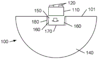
Fig. 1A-1B illustrate example contours and bottom views of a lens 100, the lens 100 including a cavity 150 for receiving a Light Emitting Device (LED) 110, and an optical element 140 that provides a desired light output pattern when light is emitted from the LED 100. In this example, the optical element 140 is a hemispherical dome that provides a substantially uniform light output pattern across its field of view.
As illustrated, to facilitate assembly, the cavity 150 is tapered and includes sloped walls 160. The bottom surface 170 of the cavity 150 is dimensioned so as to locate the light emitting device 110 at a fixed position within the cavity 150 within a given accuracy, based on the requirements of the intended application. In this example, the bottom surface 170 has substantially the same dimensions as the light emitting device, although it may be slightly larger, depending on the tolerances of the light emitting device. The required accuracy of the position of the light emitting device 110 with respect to the lens structure 100 may dictate the allowable excessive sizing (over-sizing) of the bottom surface 170, if any.
An adhesive having a refractive index equal to the refractive index of the LED110 or the lens 100, or a value between the refractive indices of the LED110 and the lens 100, may be dispersed into the cavity 150 before the LED 100 is inserted into the cavity. Depending on the particular assembly technique, the adhesive may also or alternatively be dispensed onto the LED110 prior to insertion into the cavity 150.
As illustrated in fig. 1A and 1B, a channel 180 may be provided to enable air and excess adhesive to escape during the assembly process. These passages 180 are illustrated in fig. 1A and 1B as cylindrical bores, although other shapes may be used; for example, if the cavity is formed by a molding process, the channel may have the same inclination as the inclined wall 160.
In another embodiment, the LED110 is inserted into the cavity without adhesive between the bottom surface 170 of the cavity 150 and the light emitting surface 130. A thin film of index matching liquid may be used to provide efficient optical coupling between the LED110 and the bottom surface 170. After insertion, an adhesive may be applied in the space between the LED110 and the angled wall 160. Such post-insertion application of adhesive may eliminate or minimize the need for the channel 180.
To facilitate subsequent mounting of the lens 100 with the LED110 on a subsequent substrate, such as a printed circuit board, the depth of the cavity 150 may be determined such that the contacts 120 extend slightly above ("project above" the bottom side 101) of the lens 100 when the light emitting device is fully within the cavity. A depth of about 50-500um less than the overall height of the LED110 (including the contacts 120) generally provides sufficient protrusion of the contacts beyond the bottom side 101 of the lens 100, although other depths may be used depending on the tolerance requirements of the application. For example, if the LED110 is a self-supporting chip scale package with fine tolerances, nominal protrusions as small as 5um may be used.
By shaping the taper such that the opening of the cavity 150 is larger than the size of the LED110, insertion of the LED110 into the cavity 150 is simplified. By shaping the taper such that the cross-section of the cavity 150 narrows in a direction toward the bottom surface 170, the variation in the position of the LED110 within the lens 100 is substantially controlled, thereby providing self-alignment of the LED110 as the LED110 is inserted into the lens 110. The taper also provides such self-alignment independent of the means for inserting the LED110 into the cavity 150. Even manual insertion of the LED110 into the cavity 150 will provide the same accuracy and precision as automated insertion using highly accurate and precise pick and place machines. In a similar manner, a pick and place machine of minimal accuracy and precision may be used while still maintaining the same high level of accuracy and precision.
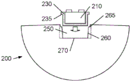
As illustrated in fig. 2, the contour of the cavity 250 of the lens 200 may be adjusted to conform to the shape of the light emitting device 210. In this example, the light emitting device 210 includes a wavelength converting layer 230, such as phosphor-embedded silicone molded over the light emitting device 210. The recess 265 at the entrance of the cavity 250 is shaped to receive the lip 235 formed by this example wavelength converting layer 230.
Below the recess 265, the cavity 250 comprises an inclined wall 260 facilitating insertion of the light emitting device 210, and a bottom surface 270 for positioning the light emitting device within the lens 200 with a given accuracy, as detailed above with respect to the surface 170 of the lens 100.
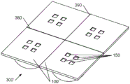
Fig. 3A and 3B illustrate example sheets 300, 300 'of lenses 100, 100' having cavities 150. Although only a few lenses 100, 100' are illustrated, those skilled in the art will recognize that the sheet 300, 300' may include hundreds of lenses 100, 100 '. For ease of illustration, the vent passage 180 of each cavity 150 of fig. 1A-1B is not illustrated, but may be present.
In the example of fig. 3A, the sheet 300 includes sixteen lenses 100, each having a single cavity 150. The sheet may comprise, for example, silicone, a silicone epoxy compound, glass, or any other transparent optical material that may be formed with a defined cavity.
In an example manufacturing process, a pick and place machine may be used to insert each LED110 (not shown) into each cavity 150. The pick and place machine may be configured to place each LED110 at the center of each cavity 150, but with sufficient compliance during insertion to enable the LED110 to be guided by the walls of the cavity 150 into a desired location. Alternatively, a pick and place machine may partially place each LED110 into each cavity 150, and a subsequent process such as a platen press may be used to complete the insertion of the LEDs 110 into the cavities 150.
In an alternative process, the LEDs are arranged on a temporary substrate at appropriate locations, such as a conventional "dicing tape", and the sheet 300 is paired with the LEDs on the substrate by overlaying the sheet 300 over the LEDs or by overlaying a dicing tape with the attached LEDs over the sheet 300.
In an example embodiment, the sheet 300 is a partially cured silicone that is cured after the LEDs 110 are inserted into each cavity 150. Subsequent curing may be used to adhere each LED110 to each lens 100, thereby avoiding the need to include a bond.
In an alternative embodiment, the sheet 300 is fully formed and an adhesive may be applied to each cavity 150 or each LED110 to secure each LED110 to each lens 100. In some embodiments, the adhesive is applied after the LED110 is inserted into the cavity 150, thereby adhering the edges of the LED110 to the walls of the cavity 150.
In other embodiments, described in detail below, the sheet 300 may comprise a material having some elasticity, and insertion of the LED110 into the cavity 150 may provide sufficient friction to maintain the LED110 in place within the lens 100.
A material that facilitates optical coupling between the light emitting surface of the LED110 and the lens 100 of the sheet 300 may be applied to the cavity 150 or the LED 110.
In a similar manner, a material for reflecting light impinging on the edges of the LED110 may be applied to the edges of the LED110, for example by filling the gap between the LED110 and the inclined walls of the cavity 150 with such a material.
After the insertion and attachment of the LED110 in the cavity 150 of the lens 100 is completed, the dicing sheet 300 may be cut along the cutting line 320 and 370 to provide a singulated LED with a lens assembly. In some embodiments, the plurality of LEDs with lenses may be provided as a single component, for example by cutting only along lines 330 and 360, thereby providing four components, each assembly comprising four LEDs with individual lenses.
Those skilled in the art will recognize that the exemplary one-to-one relationship between the LEDs and lenses of the previous figures is but one of many configurations. For example, fig. 3B illustrates an embodiment in which it is contemplated to insert multiple LEDs into multiple cavities 150 of each lens 100'. In such embodiments, the cavity 150 of each lens 100' may be more closely positioned than the cavity 150 of each lens 100 of fig. 3A.
In some embodiments, one or more of the cavities 150 may be configured to accommodate multiple LED dies, which may be arranged on a single substrate. In other embodiments, the cavity 150 within each lens 100 'may be of different sizes to accommodate a mix of different LED types within the lens 100', such as a combination of different color LEDs.
As in the example of fig. 3A, an LED110 (not shown) may be inserted into each cavity manually or via a pick and place process. Alternatively, the LEDs 110 may be disposed on a temporary substrate at locations corresponding to the cavities 150 on the sheet 300', and then the sheet 300' is mated with the substrate containing the LEDs 110. Similarly, any of the above-described techniques, or any other feasible and reliable technique, may be used to adhere the LED110 to the lens 100'.
After insertion and attachment of the LEDs 110 into the cavities 150 of each lens 100' is completed, the lenses 100' may be singulated by cutting/dicing the sheet 300' along the dicing lines 380, 390.
In view of this disclosure, those skilled in the art will recognize that the present invention is not limited to the exemplary use of a cavity 150 having linearly sloped walls 160.
Fig. 4A-4D illustrate alternative cavity profiles. 3A-3B, the exhaust passage 180 of FIG. 1 is not illustrated in these figures for ease of illustration, but may be included in each of the exemplary embodiments.
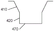
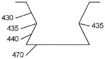
Fig. 4A illustrates a profile comprising wall segments 410, 420 having different inclinations. The upper wall segment 410 has a relatively shallow slope to provide a wide opening for insertion of an LED (not shown), while the wall segment 420 has a relatively steep slope and may be orthogonal to the surface 470 to provide a large surface area for compressing the edge of the LED to maintain proper position of the LED within the cavity.
Depending on the material forming the cavities, the closeness of fit between the size of the LEDs and the size of the surface 470, the inclination of the lower wall section 420, and the size of the vent channel 180 (not shown), this embodiment may require a great deal of force to insert each LED into each cavity. Fig. 4B-4D illustrate alternative profiles that may require a lower insertion force.
In fig. 4B, the upper wall segment 430 is tilted to provide a larger opening than the intended size of the LED, and the lower wall segment 420 is tilted in the opposite direction to create a protrusion 435 for compressing the edge of the LED to maintain the proper position of the LED within the cavity. However, as compared to fig. 4A, the edges of the LEDs will only contact these protrusions 435, not the entire surface of the lower wall segment 440. The reverse slope of the wall segments 440 provides a wider lower surface 470 than the LEDs contained between the protrusions 435, thereby providing some room for displaced air or adhesive, reducing or eliminating reliance on the exhaust channel 180.
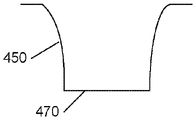
In fig. 4C, the curved wall segment 450 serves to taper the cross-sectional area in the direction of the surface 470 in a non-linear manner, such that the lower portion of the wall segment 450 may constrain the LED more than the linearly-inclined wall 160 of fig. 1, but less than the linear wall segment 420 of fig. 4A, particularly if the segment 420 is orthogonal to the surface 470. The continuous curvature of wall segment 450 may also facilitate insertion of the LED, as compared to the abrupt edge at the transition between wall segments 410 and 420 of fig. 4A.
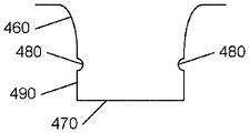
Fig. 4D illustrates the combination of curved 460 and linear 490 wall segments, and the addition of features 480 that can secure the LED while introducing minimal insertion resistance. The feature 480 may be a continuous ridge within the cavity or a plurality of individual beads from the wall segment 490. If separate protrusions are used, insertion resistance is reduced and the space between the protrusions allows displaced air and adhesive to escape, potentially avoiding the need for the vent passage 180 of FIG. 1.
In view of this disclosure, those skilled in the art will recognize that any of a wide variety of other profiles may be used to fix the position of the LED within the lens within a given tolerance while also allowing for practical insertion forces.
One skilled in the art will also recognize that the shape of the cavity or the shape of the surface of the cavity need not match the shape of the LED. Depending on the process and materials used to create the lens, it may not be economically feasible to create a rectangular cavity such as that shown in fig. 1B. Drilling or grinding a circular cavity may be far less expensive than creating a rectangular cavity if, for example, the lens is a rigid material.
Fig. 5 illustrates an example lens 500 including a conical cavity 550 having sloped walls 560 forming a circular bottom surface 570. The diameter of the surface 570 is such that it surrounds the LED110, providing a contact point 590 on the wall of the cavity that centers the LED110 at the center of the surface 570. The semi-circular gap 575 around the LED110 allows displaced air and adhesive to escape, potentially avoiding the need for the exhaust channel 180 of fig. 1.
In contrast to the rectangular surface 170 of fig. 1B, the conical cavity 550 and the circular surface 570 may allow the LED110 to rotate during the insertion process, but if the optical properties of the lens 500 are symmetric about a central axis, the rotation of the LED110 about the central axis will have no effect on the accuracy and precision of positioning the LED110 at the central axis. If the lens 500 is a partially cured silicone, the compliance of the partially cured silicone may enable the LED 100 to "penetrate" into the silicone at the corner 590, thereby controlling or limiting rotation.
It is important to note that all of the above example cross-sectional views may also be cross-sectional views of the halves of a conical cavity, although the profiles of fig. 4B and 4D would be more likely to be formed by a molding process rather than a drilling or grinding process, and it is relatively straightforward to achieve a rectangular cavity via a molding process.
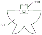
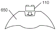
Those skilled in the art will also recognize that the optical elements of the lens are not limited to the hemispherical dome 140 of fig. 1A-1B. Fig. 6A and 6B illustrate an example side-emitting optical element 600 and an example collimating optical element 650, respectively. Other optical elements may be used to achieve the desired light output pattern.
While the invention has been illustrated and described in detail in the drawings and foregoing description, such illustration and description are to be considered illustrative or exemplary and not restrictive; the invention is not limited to the disclosed embodiments.
For example, it is possible to operate the invention in embodiments in which additional elements may be included within the cavity. For example, the wavelength converting material may be inserted into the cavity before the light emitting device is inserted. Alternatively or additionally, the lens may comprise a wavelength converting material, or the light emitting device may comprise a wavelength converting material. In some embodiments, the wavelength converting material may be used as an adhesive layer between the light emitting device and the lens.
Other variations to the disclosed embodiments can be understood and effected by those skilled in the art in practicing the claimed invention, from a study of the drawings, the disclosure, and the appended claims. In the claims, the word "comprising" does not exclude other elements or steps, and the indefinite article "a" or "an" does not exclude a plurality. The mere fact that certain measures are recited in mutually different dependent claims does not indicate that a combination of these measures cannot be used to advantage. Any reference signs in the claims shall not be construed as limiting the scope.
Claims (15)
1. A lens structure, comprising:
a cavity having an opening for receiving a light emitting device, the cavity having a taper such that the cross-sectional area within the cavity is smaller than the area of the opening, an
An optical element that provides a specific light output pattern when illuminated by a light emitting device within the cavity.
2. The lens structure of claim 1, wherein the cone comprises one or more walls that are linearly sloped.
3. The lens structure of claim 2, wherein the taper enables the light emitting device to be disposed at a fixed location within the lens structure.
4. The lens structure of claim 1, wherein the depth of the cavity is such that electrical contacts of the light emitting device protrude from the cavity when the light emitting device is fully inserted into the cavity.
5. The lens structure of claim 1, wherein the cone comprises a compound form.
6. The lens structure of claim 1, wherein the taper comprises one or more curved walls.
7. The lens structure of claim 1, comprising one or more channels that allow displacement of the material when the light emitting device is inserted in the cavity.
8. The lens structure of claim 1, comprising one or more protrusions within the cavity for reducing the cross-sectional area.
9. The lens structure of claim 1, comprising a light emitting device and a reflective material between a wall of the cavity and an edge of the light emitting device.
10. A sheet, comprising:
a plurality of lens structures, each lens structure having one or more tapered cavities for receiving a light emitting element and an optical element providing a particular light output pattern when the light emitting element emits light,
wherein each tapered cavity has an opening for receiving a light emitting element, a surface to which the light emitting element is optically coupled, and at least one cross-sectional area that is smaller than the cross-sectional area of the opening.
11. The sheet of claim 10, wherein the sheet comprises a silicone material.
12. The sheet of claim 11, wherein the sheet comprises a plurality of light emitting elements in each cavity and the silicone material is in a partially cured state.
13. The sheet of claim 10, wherein the sheet comprises glass.
14. A method for creating a light emitting product, comprising:
providing a sheet comprising a plurality of lens structures, each lens structure having one or more tapered cavities for receiving a light emitting element and an optical element providing a particular light output pattern when the light emitting element emits light, and each tapered cavity having an opening for receiving the light emitting element, a surface to which the light emitting element is optically coupled, and at least one cross-sectional area that is smaller than the cross-sectional area of the opening;
inserting a light emitting element into each tapered cavity; and
the lens structures with corresponding light emitting elements are singulated to form light emitting products.
15. The method of claim 14, wherein the sheet comprises silicone in an at least partially cured state when the light emitting elements are inserted into the cavities, and the method comprises curing the silicone after the light emitting elements are inserted into the cavities.
Applications Claiming Priority (3)
| Application Number | Priority Date | Filing Date | Title |
|---|---|---|---|
| US201461930586P | 2014-01-23 | 2014-01-23 | |
| US61/930586 | 2014-01-23 | ||
| CN201580005512.XA CN105940262B (en) | 2014-01-23 | 2015-01-04 | Light emitting device with self-aligned preformed lens |
Related Parent Applications (1)
| Application Number | Title | Priority Date | Filing Date |
|---|---|---|---|
| CN201580005512.XA Division CN105940262B (en) | 2014-01-23 | 2015-01-04 | Light emitting device with self-aligned preformed lens |
Publications (1)
| Publication Number | Publication Date |
|---|---|
| CN111063787A true CN111063787A (en) | 2020-04-24 |
Family
ID=52396775
Family Applications (2)
| Application Number | Title | Priority Date | Filing Date |
|---|---|---|---|
| CN201911355103.9A Pending CN111063787A (en) | 2014-01-23 | 2015-01-04 | Light emitting device with self-aligned preformed lens |
| CN201580005512.XA Active CN105940262B (en) | 2014-01-23 | 2015-01-04 | Light emitting device with self-aligned preformed lens |
Family Applications After (1)
| Application Number | Title | Priority Date | Filing Date |
|---|---|---|---|
| CN201580005512.XA Active CN105940262B (en) | 2014-01-23 | 2015-01-04 | Light emitting device with self-aligned preformed lens |
Country Status (6)
| Country | Link |
|---|---|
| US (3) | US10416356B2 (en) |
| EP (1) | EP3097351A1 (en) |
| JP (2) | JP2017504215A (en) |
| KR (1) | KR102217791B1 (en) |
| CN (2) | CN111063787A (en) |
| WO (1) | WO2015110927A1 (en) |
Cited By (1)
| Publication number | Priority date | Publication date | Assignee | Title |
|---|---|---|---|---|
| US10895669B2 (en) | 2014-01-23 | 2021-01-19 | Lumileds Llc | Light emitting device with self-aligning preformed lens |
Families Citing this family (5)
| Publication number | Priority date | Publication date | Assignee | Title |
|---|---|---|---|---|
| JP6645781B2 (en) * | 2015-09-11 | 2020-02-14 | アルパッド株式会社 | Semiconductor light emitting device |
| US10340173B2 (en) * | 2016-10-11 | 2019-07-02 | Micron Technology, Inc. | System for handling semiconductor dies |
| DE102017122325A1 (en) | 2017-09-26 | 2019-03-28 | Osram Opto Semiconductors Gmbh | Radiation-emitting semiconductor component and method for producing radiation-emitting semiconductor components |
| KR20190120715A (en) * | 2018-04-16 | 2019-10-24 | 리지텍 일렉트로닉스 컴퍼니 리미티드 | Structured light projection system |
| EP3832199A1 (en) * | 2019-12-06 | 2021-06-09 | Marelli Automotive Lighting Italy S.p.A. | Automotive lighting and/or signaling device and related assembly method |
Citations (26)
| Publication number | Priority date | Publication date | Assignee | Title |
|---|---|---|---|---|
| US20010026011A1 (en) * | 1999-03-15 | 2001-10-04 | Roberts John K. | Radiation emitter devices and method of making the same |
| US20020080615A1 (en) * | 2000-12-22 | 2002-06-27 | Thomas Marshall | LED collimation optics with improved performance and reduced size |
| US20020163810A1 (en) * | 2001-05-04 | 2002-11-07 | West Robert S. | Side emitting LED |
| US20020163808A1 (en) * | 2001-05-04 | 2002-11-07 | West Robert S. | Lens and Lens Cap with Sawtooth Portion for Light Emitting Diode |
| JP2005159149A (en) * | 2003-11-27 | 2005-06-16 | Aoki Denki Kogyo Kk | High luminance led emission part |
| CN1726410A (en) * | 2002-10-11 | 2006-01-25 | 光处方革新有限公司 | Compact folded-optics illumination lens |
| US20060078246A1 (en) * | 2004-10-07 | 2006-04-13 | Towa Corporation | Transparent member, optical device using transparent member and method of manufacturing optical device |
| JP2007059618A (en) * | 2005-08-24 | 2007-03-08 | Matsushita Electric Works Ltd | Led light fixture |
| CN1934722A (en) * | 2004-03-24 | 2007-03-21 | 东芝照明技术株式会社 | Light-emitting device |
| US7349163B2 (en) * | 2001-12-06 | 2008-03-25 | Fraen Corporation S.R.L. | High-heat-dissipation lighting module |
| CN101240885A (en) * | 2007-12-10 | 2008-08-13 | 王敏 | LED small angle long distance optical lens and array |
| US20080203415A1 (en) * | 2007-02-13 | 2008-08-28 | 3M Innovative Properties Company | Led devices having lenses and methods of making same |
| US20080283861A1 (en) * | 2004-06-04 | 2008-11-20 | Cree, Inc. | Power light emitting die package with reflecting lens and the method of making the same |
| CN101636851A (en) * | 2007-02-26 | 2010-01-27 | 皇家菲利浦电子有限公司 | Have phosphor sheet and the LED that crosses the mold pressing phosphor in the lens |
| JP2010170734A (en) * | 2009-01-20 | 2010-08-05 | Panasonic Electric Works Co Ltd | Led lighting system |
| US7874703B2 (en) * | 2008-08-28 | 2011-01-25 | Dialight Corporation | Total internal reflection lens with base |
| CN102017199A (en) * | 2008-04-24 | 2011-04-13 | 松下电工株式会社 | Light emitting unit with lens |
| CN102052630A (en) * | 2009-11-09 | 2011-05-11 | 富准精密工业(深圳)有限公司 | Light-emitting assembly |
| JP2011113755A (en) * | 2009-11-25 | 2011-06-09 | Panasonic Electric Works Co Ltd | Light emitting device |
| CN102563525A (en) * | 2010-11-10 | 2012-07-11 | 三星Led株式会社 | Flash lens and flash module employing the same |
| CN102686935A (en) * | 2009-12-21 | 2012-09-19 | 马丁专业公司 | Light collector with complementing rotationally asymmetric central and peripheral lenses |
| CN102800797A (en) * | 2011-05-24 | 2012-11-28 | 台湾积体电路制造股份有限公司 | Batwing led with remote phosphor configuration |
| US20130039050A1 (en) * | 2011-08-08 | 2013-02-14 | Quarkstar, Llc | Solid-State Luminaire |
| CN103196040A (en) * | 2012-01-06 | 2013-07-10 | 扬升照明股份有限公司 | Lens structure, light source device and light source module |
| US20130235581A1 (en) * | 2010-10-27 | 2013-09-12 | Dbm Reflex Enterprises Inc. | Lens array assembly for solid state light sources and method |
| US20140377894A1 (en) * | 2013-06-25 | 2014-12-25 | Samsung Electronics Co., Ltd. | Method of manufacturing semiconductor light emitting device package |
Family Cites Families (41)
| Publication number | Priority date | Publication date | Assignee | Title |
|---|---|---|---|---|
| NO143045B (en) | 1975-05-16 | Kolbjoern Bjoershol | APPLIANCE FOR CROCHETING A FISHING LINE. | |
| JPS5860954A (en) * | 1981-10-07 | 1983-04-11 | Asahimatsu Shokuhin Kk | Preparation of gelatinous food of freeze-denaturated soybean protein |
| JPS5860954U (en) | 1981-10-19 | 1983-04-25 | 株式会社リコー | Light emitting element mounting structure |
| JPH0561790U (en) * | 1992-01-21 | 1993-08-13 | セイコーエプソン株式会社 | control panel |
| JPH06104491A (en) * | 1992-09-17 | 1994-04-15 | Rohm Co Ltd | Light emitting sdiode lamp |
| JPH11204841A (en) | 1998-01-13 | 1999-07-30 | Nichia Chem Ind Ltd | Photo-semiconductor device and its manufacture |
| JP3349111B2 (en) * | 1999-03-15 | 2002-11-20 | 株式会社シチズン電子 | Surface mount type light emitting diode and method of manufacturing the same |
| JP3948650B2 (en) | 2001-10-09 | 2007-07-25 | アバゴ・テクノロジーズ・イーシービーユー・アイピー(シンガポール)プライベート・リミテッド | Light emitting diode and manufacturing method thereof |
| US7465961B2 (en) * | 2003-03-25 | 2008-12-16 | Sharp Kabushiki Kaisha | Electronic equipment, backlight structure and keypad for electronic equipment |
| US7009213B2 (en) | 2003-07-31 | 2006-03-07 | Lumileds Lighting U.S., Llc | Light emitting devices with improved light extraction efficiency |
| JP4444609B2 (en) | 2003-09-26 | 2010-03-31 | スタンレー電気株式会社 | LED lamp and manufacturing method |
| US7452737B2 (en) | 2004-11-15 | 2008-11-18 | Philips Lumileds Lighting Company, Llc | Molded lens over LED die |
| KR100649640B1 (en) * | 2005-02-03 | 2006-11-27 | 삼성전기주식회사 | Side emission type led package |
| TW200825529A (en) * | 2006-12-06 | 2008-06-16 | Chi Lin Technology Co Ltd | Light mixer and backlight module having it |
| US7993034B2 (en) * | 2007-09-21 | 2011-08-09 | Cooper Technologies Company | Reflector having inflection point and LED fixture including such reflector |
| CN101235953A (en) | 2008-03-04 | 2008-08-06 | 友达光电股份有限公司 | Lens structure and light emitting unit |
| EP2260341A2 (en) * | 2008-03-05 | 2010-12-15 | Oree, Advanced Illumination Solutions INC. | Illumination apparatus and methods of forming the same |
| DE102008025756B4 (en) * | 2008-05-29 | 2023-02-23 | OSRAM Opto Semiconductors Gesellschaft mit beschränkter Haftung | semiconductor device |
| BRPI0913195A2 (en) | 2008-05-30 | 2016-01-12 | Sharp Kk | light emitting device, surface light source, liquid crystal display device and method for manufacturing light emitting device |
| CN101936501B (en) * | 2009-06-30 | 2013-04-24 | 富准精密工业(深圳)有限公司 | Light emitting diode module |
| US8803171B2 (en) * | 2009-07-22 | 2014-08-12 | Koninklijke Philips N.V. | Reduced color over angle variation LEDs |
| US9385285B2 (en) | 2009-09-17 | 2016-07-05 | Koninklijke Philips N.V. | LED module with high index lens |
| CN102062347A (en) * | 2009-11-12 | 2011-05-18 | 富准精密工业(深圳)有限公司 | Light-emitting diode module and lens thereof |
| JP5701502B2 (en) * | 2009-12-25 | 2015-04-15 | 日亜化学工業株式会社 | Light emitting device |
| JP5512262B2 (en) * | 2009-12-26 | 2014-06-04 | 株式会社朝日ラバー | Lens array sheet and dicing method thereof |
| JP5449039B2 (en) | 2010-06-07 | 2014-03-19 | 株式会社東芝 | Semiconductor light emitting device and manufacturing method thereof |
| US8597988B2 (en) * | 2010-11-18 | 2013-12-03 | Bridgelux, Inc. | System for flash-free overmolding of led array substrates |
| TW201233940A (en) | 2010-11-30 | 2012-08-16 | Wintek Corp | Light source for crystal lamp |
| JP5897554B2 (en) * | 2011-04-28 | 2016-03-30 | 株式会社朝日ラバー | Optical semiconductor device with lens and manufacturing method thereof |
| KR20120133264A (en) | 2011-05-31 | 2012-12-10 | 삼성전자주식회사 | Lens for light emitting diode, light emitting diode module comprising the same and method for manufacturing light emitting diode module using the same |
| WO2013084155A1 (en) | 2011-12-08 | 2013-06-13 | Koninklijke Philips Electronics N.V. | Forming thick metal layers on a semiconductor light emitting device |
| CN103187504A (en) * | 2011-12-27 | 2013-07-03 | 展晶科技(深圳)有限公司 | Package structure of light emitting diode |
| JP6309898B2 (en) * | 2012-01-16 | 2018-04-11 | ダウ シリコーンズ コーポレーション | Optical article and forming method |
| KR101386710B1 (en) | 2012-04-05 | 2014-04-18 | 건국대학교 산학협력단 | Use of acyclic succinoglycan dimer |
| US9349929B2 (en) * | 2012-05-31 | 2016-05-24 | Cree, Inc. | Light emitter packages, systems, and methods |
| TW201431127A (en) * | 2013-01-29 | 2014-08-01 | Hon Hai Prec Ind Co Ltd | LED package and a method for manufacturing the same |
| US9318674B2 (en) * | 2013-02-05 | 2016-04-19 | Cree, Inc. | Submount-free light emitting diode (LED) components and methods of fabricating same |
| KR102217791B1 (en) | 2014-01-23 | 2021-02-22 | 루미리즈 홀딩 비.브이. | Light emitting device with self-aligning preformed lens |
| US10297731B2 (en) * | 2014-11-26 | 2019-05-21 | Bridgelux, Inc. | Light emitting diode constructions and methods for making the same |
| US10591134B2 (en) * | 2016-01-19 | 2020-03-17 | Lutron Ketra, Llc | Lens for improved color mixing and beam control of an LED light source |
| JP6104491B1 (en) | 2017-01-20 | 2017-03-29 | 三菱日立パワーシステムズ株式会社 | Ship desulfurization apparatus and ship equipped with the ship desulfurization apparatus |
-
2015
- 2015-01-04 KR KR1020167023018A patent/KR102217791B1/en active IP Right Grant
- 2015-01-04 WO PCT/IB2015/050050 patent/WO2015110927A1/en active Application Filing
- 2015-01-04 EP EP15701247.7A patent/EP3097351A1/en not_active Withdrawn
- 2015-01-04 JP JP2016547552A patent/JP2017504215A/en active Pending
- 2015-01-04 CN CN201911355103.9A patent/CN111063787A/en active Pending
- 2015-01-04 CN CN201580005512.XA patent/CN105940262B/en active Active
- 2015-01-04 US US15/110,840 patent/US10416356B2/en active Active
-
2019
- 2019-09-16 US US16/572,074 patent/US10895669B2/en active Active
-
2020
- 2020-09-30 JP JP2020164629A patent/JP2021002682A/en active Pending
-
2021
- 2021-01-14 US US17/149,129 patent/US11313996B2/en active Active
Patent Citations (28)
| Publication number | Priority date | Publication date | Assignee | Title |
|---|---|---|---|---|
| US20030168670A1 (en) * | 1999-03-15 | 2003-09-11 | Roberts John K. | Method of making radiation emitter devices |
| US20010026011A1 (en) * | 1999-03-15 | 2001-10-04 | Roberts John K. | Radiation emitter devices and method of making the same |
| US20020080615A1 (en) * | 2000-12-22 | 2002-06-27 | Thomas Marshall | LED collimation optics with improved performance and reduced size |
| CN1404630A (en) * | 2000-12-22 | 2003-03-19 | 皇家菲利浦电子有限公司 | LED module |
| US20020163810A1 (en) * | 2001-05-04 | 2002-11-07 | West Robert S. | Side emitting LED |
| US20020163808A1 (en) * | 2001-05-04 | 2002-11-07 | West Robert S. | Lens and Lens Cap with Sawtooth Portion for Light Emitting Diode |
| US7349163B2 (en) * | 2001-12-06 | 2008-03-25 | Fraen Corporation S.R.L. | High-heat-dissipation lighting module |
| CN1726410A (en) * | 2002-10-11 | 2006-01-25 | 光处方革新有限公司 | Compact folded-optics illumination lens |
| JP2005159149A (en) * | 2003-11-27 | 2005-06-16 | Aoki Denki Kogyo Kk | High luminance led emission part |
| CN1934722A (en) * | 2004-03-24 | 2007-03-21 | 东芝照明技术株式会社 | Light-emitting device |
| US20080283861A1 (en) * | 2004-06-04 | 2008-11-20 | Cree, Inc. | Power light emitting die package with reflecting lens and the method of making the same |
| US20060078246A1 (en) * | 2004-10-07 | 2006-04-13 | Towa Corporation | Transparent member, optical device using transparent member and method of manufacturing optical device |
| JP2007059618A (en) * | 2005-08-24 | 2007-03-08 | Matsushita Electric Works Ltd | Led light fixture |
| US20080203415A1 (en) * | 2007-02-13 | 2008-08-28 | 3M Innovative Properties Company | Led devices having lenses and methods of making same |
| CN101636851A (en) * | 2007-02-26 | 2010-01-27 | 皇家菲利浦电子有限公司 | Have phosphor sheet and the LED that crosses the mold pressing phosphor in the lens |
| CN101240885A (en) * | 2007-12-10 | 2008-08-13 | 王敏 | LED small angle long distance optical lens and array |
| CN102017199A (en) * | 2008-04-24 | 2011-04-13 | 松下电工株式会社 | Light emitting unit with lens |
| US7874703B2 (en) * | 2008-08-28 | 2011-01-25 | Dialight Corporation | Total internal reflection lens with base |
| JP2010170734A (en) * | 2009-01-20 | 2010-08-05 | Panasonic Electric Works Co Ltd | Led lighting system |
| CN102052630A (en) * | 2009-11-09 | 2011-05-11 | 富准精密工业(深圳)有限公司 | Light-emitting assembly |
| JP2011113755A (en) * | 2009-11-25 | 2011-06-09 | Panasonic Electric Works Co Ltd | Light emitting device |
| CN102686935A (en) * | 2009-12-21 | 2012-09-19 | 马丁专业公司 | Light collector with complementing rotationally asymmetric central and peripheral lenses |
| US20130235581A1 (en) * | 2010-10-27 | 2013-09-12 | Dbm Reflex Enterprises Inc. | Lens array assembly for solid state light sources and method |
| CN102563525A (en) * | 2010-11-10 | 2012-07-11 | 三星Led株式会社 | Flash lens and flash module employing the same |
| CN102800797A (en) * | 2011-05-24 | 2012-11-28 | 台湾积体电路制造股份有限公司 | Batwing led with remote phosphor configuration |
| US20130039050A1 (en) * | 2011-08-08 | 2013-02-14 | Quarkstar, Llc | Solid-State Luminaire |
| CN103196040A (en) * | 2012-01-06 | 2013-07-10 | 扬升照明股份有限公司 | Lens structure, light source device and light source module |
| US20140377894A1 (en) * | 2013-06-25 | 2014-12-25 | Samsung Electronics Co., Ltd. | Method of manufacturing semiconductor light emitting device package |
Cited By (2)
| Publication number | Priority date | Publication date | Assignee | Title |
|---|---|---|---|---|
| US10895669B2 (en) | 2014-01-23 | 2021-01-19 | Lumileds Llc | Light emitting device with self-aligning preformed lens |
| US11313996B2 (en) | 2014-01-23 | 2022-04-26 | Lumileds Llc | Light emitting device with self-aligning preformed lens |
Also Published As
| Publication number | Publication date |
|---|---|
| JP2021002682A (en) | 2021-01-07 |
| US20200116902A1 (en) | 2020-04-16 |
| JP2017504215A (en) | 2017-02-02 |
| US10416356B2 (en) | 2019-09-17 |
| KR102217791B1 (en) | 2021-02-22 |
| US10895669B2 (en) | 2021-01-19 |
| KR20160113198A (en) | 2016-09-28 |
| EP3097351A1 (en) | 2016-11-30 |
| CN105940262A (en) | 2016-09-14 |
| CN105940262B (en) | 2020-01-07 |
| WO2015110927A1 (en) | 2015-07-30 |
| US20210132263A1 (en) | 2021-05-06 |
| US11313996B2 (en) | 2022-04-26 |
| US20160341852A1 (en) | 2016-11-24 |
Similar Documents
| Publication | Publication Date | Title |
|---|---|---|
| US11313996B2 (en) | Light emitting device with self-aligning preformed lens | |
| US9018663B2 (en) | Lens-equipped optical semiconductor device and method for manufacturing the same | |
| KR101219106B1 (en) | Light emitting device package and methdod of manufacturing the same | |
| JP4744573B2 (en) | Manufacturing method of electronic device | |
| TWI408835B (en) | Over molded over led die | |
| EP2666193B1 (en) | Led package comprising encapsulation | |
| EP3044809B1 (en) | Frame based package for flip-chip led | |
| TW201042780A (en) | Compact molded LED module | |
| US20150287891A1 (en) | LED Packaging Structure Using Distant Fluorescent Powder Layer and Manufacturing Method Thereof | |
| EP2973759B1 (en) | Encapsulating led lens with bottom reflectors | |
| EP2177337A1 (en) | Optical device molding system | |
| KR20130013468A (en) | Method of manufacturing light emitting device | |
| CN105393372A (en) | LED dome with inner high index pillar | |
| US8828754B2 (en) | Method for manufacturing LED | |
| CN105845790A (en) | Flip chip LED chip packaging method and packaging groove mould | |
| US8956893B2 (en) | Metiod of making LED with bat-wing emitting field lens | |
| JP5189925B2 (en) | Lens member manufacturing method | |
| CN117239018A (en) | Preparation method of ultraviolet LED device |
Legal Events
| Date | Code | Title | Description |
|---|---|---|---|
| PB01 | Publication | ||
| PB01 | Publication | ||
| SE01 | Entry into force of request for substantive examination | ||
| SE01 | Entry into force of request for substantive examination |