Disclosure of Invention
The embodiment of the application provides a display panel, a preparation method thereof and a display device, which can reduce the loss of an organic photoresist layer in the process of dry etching of source/drain wirings, and further avoid the breakage of the source/drain wirings.
In order to solve the above problem, in a first aspect, the present application provides a display panel, the display panel includes the display area and is located the bending area in the display area outside, the display panel includes source electrode/drain electrode metal level in the bending area, the display panel includes organic photoresist layer, organic photoresist layer is close to one side of source electrode/drain electrode metal level is equipped with bending area interlayer dielectric layer.
The source/drain metal layer comprises source/drain metal lines which are arranged at intervals along a direction parallel to the surface of the display panel; in the bending region, the bending region interlayer dielectric layer is positioned in the projection region of the source/drain metal wire, and the thickness of the bending region interlayer dielectric layer is a first preset value.
In the display area, a first interlayer dielectric layer of the display area, a second interlayer dielectric layer of the display area, a grid metal layer and a grid insulating layer of the display area are sequentially arranged on one side, close to the organic light resistance layer, of the source/drain metal layer; the surface of one side, far away from the source/drain metal layer, of the first interlayer dielectric layer in the display area is flush with the surface of one side, far away from the source/drain metal layer, of the interlayer dielectric layer in the bending area.
In the projection area of the source electrode/drain electrode metal wire, the thickness of a first interlayer dielectric layer in the display area is the first preset value; and between the projection areas of the source/drain metal lines, the thickness of the first interlayer dielectric layer in the display area is a second preset value, wherein the first preset value is larger than the second preset value.
The display area first interlayer dielectric layer and the bending area interlayer dielectric layer form a film layer at a first preset temperature, the display area second interlayer dielectric layer forms a film layer at a second preset temperature, and the first preset temperature is lower than the second preset temperature.
In order to solve the above problem, in a second aspect, the present application provides a display device including the display panel of any one of the above.
In order to solve the above problem, in a third aspect, the present application provides a method for manufacturing a display panel, where the display panel includes a display area and a bending area located outside the display area, the method including:
preparing an organic photoresist layer in the bending area of the display panel;
preparing a bending region interlayer dielectric layer on the organic photoresist layer;
and preparing a source electrode/drain electrode metal layer on the bending region interlayer dielectric layer, wherein the bending region interlayer dielectric layer is used for reducing the loss of the organic photoresist layer when the source electrode/drain electrode metal layer is prepared.
The preparation of the bending area interlayer dielectric layer on the organic photoresist layer comprises the following steps:
preparing the bending area interlayer dielectric layer with the thickness of a first preset value on the organic photoresist layer;
the preparation of the source/drain metal layer on the bending region interlayer dielectric layer comprises the following steps:
and preparing source/drain metal wires which are arranged at intervals in a direction parallel to the surface of the display panel by a dry etching process, and etching the thickness of the interlayer dielectric layer of the bending region between the projection regions of the source/drain metal wires to a second preset value.
Wherein, the preparing of the organic photoresist layer in the bending area of the display panel comprises:
sequentially preparing a display area grid insulating layer, a grid metal layer and a display area second interlayer dielectric layer in the display area of the display panel, and preparing the organic photoresist layer in the bending area of the display panel;
the preparation of the bending area interlayer dielectric layer on the organic photoresist layer comprises the following steps:
and preparing a first interlayer dielectric layer on the surfaces of the second interlayer dielectric layer in the display area and the organic photoresist layer, wherein the first interlayer dielectric layer comprises a first interlayer dielectric layer in the display area and a bending area interlayer dielectric layer in the bending area, and the surface of one side, close to the second interlayer dielectric layer in the display area, of the first interlayer dielectric layer in the display area is flush with the surface of one side, close to the organic photoresist layer, of the bending area interlayer dielectric layer.
Wherein the first preset temperature is lower than the second preset temperature,
the method for sequentially preparing a display area grid insulating layer, a grid metal layer and a display area second interlayer dielectric layer in the display area of the display panel comprises the following steps:
preparing a second interlayer dielectric layer of the display area at the second preset temperature;
preparing a first interlayer dielectric layer on the surfaces of the second interlayer dielectric layer and the organic photoresist layer in the display area, wherein the preparation method comprises the following steps:
and preparing the first interlayer dielectric layer at the first preset temperature.
The beneficial effect of this application is: being different from the prior art, the application provides a display panel, and this display panel includes display area and the bending region that is located the display area outside, and display panel includes source electrode/drain electrode metal level, and in the bending region, display panel includes organic photoresist layer, and the organic photoresist layer is close to one side of source electrode/drain electrode metal level and is equipped with bending region interlayer dielectric layer. According to the method, the bending region interlayer dielectric layer is arranged between the source/drain electrode metal layer and the organic photoresist layer, so that the loss of the organic photoresist layer in the process of dry etching of the source/drain electrode wiring can be reduced, and the breakage of the source/drain electrode wiring is avoided.
DETAILED DESCRIPTION OF EMBODIMENT (S) OF INVENTION
The technical solutions in the embodiments of the present application will be clearly and completely described below with reference to the drawings in the embodiments of the present application, and it is obvious that the described embodiments are only a part of the embodiments of the present application, and not all of the embodiments. All other embodiments, which can be derived by a person skilled in the art from the embodiments given herein without making any creative effort, shall fall within the protection scope of the present application.
In the description of the present application, it is to be understood that the terms "center", "longitudinal", "lateral", "length", "width", "thickness", "upper", "lower", "front", "rear", "left", "right", "vertical", "horizontal", "top", "bottom", "inner", "outer", and the like indicate orientations or positional relationships based on those shown in the drawings, and are used merely for convenience of description and for simplicity of description, and do not indicate or imply that the referenced device or element must have a particular orientation, be constructed in a particular orientation, and be operated, and thus should not be considered as limiting the present application. Furthermore, the terms "first", "second" and "first" are used for descriptive purposes only and are not to be construed as indicating or implying relative importance or implicitly indicating the number of technical features indicated. Thus, a feature defined as "first" or "second" may explicitly or implicitly include one or more features. In the description of the present application, "a plurality" means two or more unless specifically limited otherwise.
In this application, the word "exemplary" is used to mean "serving as an example, instance, or illustration. Any embodiment described herein as "exemplary" is not necessarily to be construed as preferred or advantageous over other embodiments. The following description is presented to enable any person skilled in the art to make and use the application. In the following description, details are set forth for the purpose of explanation. It will be apparent to one of ordinary skill in the art that the present application may be practiced without these specific details. In other instances, well-known structures and processes are not set forth in detail in order to avoid obscuring the description of the present application with unnecessary detail. Thus, the present application is not intended to be limited to the embodiments shown, but is to be accorded the widest scope consistent with the principles and features disclosed herein.
The embodiment of the application provides a display panel, the display panel includes display area and the bending region that is located the display area outside, the display panel includes source electrode/drain electrode metal level, in the bending region, the display panel includes organic photoresist layer, one side that organic photoresist layer is close to source electrode/drain electrode metal level is equipped with bending region interlaminar dielectric layer. The display panel of the embodiment of the application can be applied to various display devices. The details will be described below.
Referring to fig. 1, fig. 1 is a schematic structural diagram of an embodiment of a display panel according to the present application.
In this embodiment, the display panel 10 includes a display area 11 and a bending area 12 located outside the display area 11. The display panel 10 includes a source/drain metal layer 140. In the bending region 12, the display panel 10 includes an organic photoresist layer 121, and a bending region interlayer dielectric layer 132 is disposed on a side of the organic photoresist layer 121 close to the source/drain metal layer 140.
In this embodiment, the organic photoresist layer 121 is filled with an organic photoresist, and the material of the interlayer dielectric layer 132 in the bending region is silicon nitride, silicon oxide or a composite of the two. In other embodiments, the materials of the organic photoresist layer 121 and the bending region interlayer dielectric layer 132 may be selected according to specific situations, which are not limited in this application. The organic photoresist layer 121 is disposed in the bending region 12 of the display panel 10, so that the bending resistance of the display panel 10 can be improved. The bending region interlayer dielectric layer 132 is disposed between the source/drain metal layer 140 and the organic photoresist layer 121, so that the loss of the organic photoresist layer 121 in the dry etching process of the source/drain trace can be reduced, and the source/drain trace can be prevented from being broken.
Being different from the prior art, the application provides a display panel, and this display panel includes display area and the bending region that is located the display area outside, and display panel includes source electrode/drain electrode metal level, and in the bending region, display panel includes organic photoresist layer, and the organic photoresist layer is close to one side of source electrode/drain electrode metal level and is equipped with bending region interlayer dielectric layer. According to the method, the bending region interlayer dielectric layer is arranged between the source/drain electrode metal layer and the organic photoresist layer, so that the loss of the organic photoresist layer in the process of dry etching of the source/drain electrode wiring can be reduced, and the breakage of the source/drain electrode wiring is avoided.
For describing the structure of the display panel of the present application in detail, please refer to fig. 2, and fig. 2 is a schematic structural diagram of another embodiment of the display panel according to the present application.
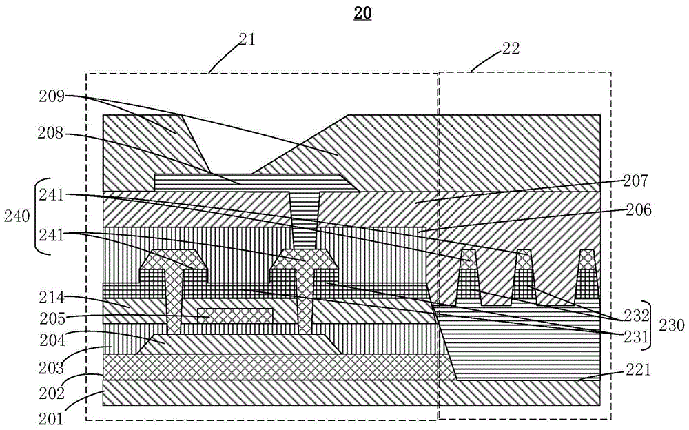
In this embodiment, the display panel 20 includes a display area 21 and a bending area 22 located outside the display area 21. The display panel 20 includes a source/drain metal layer 240, and in the bending region 22, the display panel 20 includes an organic photoresist layer 221, and a bending region interlayer dielectric layer 232 is disposed on a side of the organic photoresist layer 221 close to the source/drain metal layer 240.
In this embodiment, the source/drain metal layer 240 includes source/drain metal lines 241 arranged at intervals along a direction parallel to the surface of the display panel 20. In the bending region 22, the bending region interlayer dielectric layer 232 is located in the projection region of the source/drain metal line 241, and the thickness of the bending region interlayer dielectric layer 232 is a first predetermined value. The first preset value may be any value greater than 0, for example, the first preset value is greater than 0 and does not exceed 200 nm, and may be set according to specific situations. Preferably, the first predetermined value is greater than a loss thickness of the kink region interlayer dielectric layer 232 during the preparation of the source/drain metal line 241. The first preset value is greater than the loss thickness of the bending region interlayer dielectric layer 232 when the source/drain metal line 241 is prepared, and after the source/drain metal line 241 is prepared, the bending region interlayer dielectric layer 232 still keeps a certain thickness, so that the loss of the organic photoresist layer 221 when the source/drain metal line 241 is prepared can be avoided. In addition, the loss thickness of the organic photoresist layer 221 can be controlled by controlling the first predetermined value, so as to improve the bending resistance of the source/drain metal line 241.
In the present embodiment, in the display region 21, the source/drain metal layer 240 is disposed on a side close to the organic photoresist layer 221, and the display region first interlayer dielectric layer 231, the display region second interlayer dielectric layer 214, the gate metal layer 205 and the display region gate insulating layer 203 are sequentially disposed. The surface of the first interlayer dielectric layer 231 in the display region away from the source/drain metal layer 240 is flush with the surface of the interlayer dielectric layer 232 in the bending region away from the source/drain metal layer 240. Specifically, the first interlayer dielectric layer 230 is prepared through a single process, and the first interlayer dielectric layer 230 includes a display region first interlayer dielectric layer 231 and a bending region interlayer dielectric layer 232. The first interlayer dielectric layer 231 in the display area and the interlayer dielectric layer 232 in the bending area are prepared by one process, so that the process complexity is reduced, and the preparation efficiency is improved.
Furthermore, an active layer 204, a buffer layer 202 and a substrate 201 are sequentially disposed on a side of the gate insulating layer 203 of the display area away from the gate metal layer 205.
Further, in the projection region of the source/drain metal line 241, the thickness of the first interlayer dielectric layer 231 in the display region is a first preset value. The thickness of the first interlayer dielectric layer 231 in the display region between the projection regions of the source/drain metal lines 241 is a second predetermined value, wherein the first predetermined value is greater than the second predetermined value.
In this embodiment, the first interlayer dielectric layer 231 and the bending interlayer dielectric layer 232 in the display region form a film at a first predetermined temperature, and the second interlayer dielectric layer 214 in the display region forms a film at a second predetermined temperature, where the first predetermined temperature is lower than the second predetermined temperature. That is, the first interlayer dielectric layer 231 and the bending interlayer dielectric layer 232 in the display region are formed at a low temperature, the second interlayer dielectric layer 214 in the display region is formed at a high temperature, and the first interlayer dielectric layer 231 and the bending interlayer dielectric layer 232 in the display region are formed at a low temperature, so that the organic photoresist layer 221 is prevented from being damaged by the high temperature.
Being different from the prior art, the application provides a display panel, and this display panel includes display area and the bending region that is located the display area outside, and display panel includes source electrode/drain electrode metal level, and in the bending region, display panel includes organic photoresist layer, and the organic photoresist layer is close to one side of source electrode/drain electrode metal level and is equipped with bending region interlayer dielectric layer. According to the method, the bending region interlayer dielectric layer is arranged between the source/drain electrode metal layer and the organic photoresist layer, so that the loss of the organic photoresist layer in the process of dry etching of the source/drain electrode wiring can be reduced, and the breakage of the source/drain electrode wiring is avoided.
Referring to fig. 3-10, fig. 3 is a schematic flow chart illustrating an embodiment of a method for manufacturing a display panel according to an embodiment of the present disclosure; FIG. 4 is a schematic structural diagram of the display panel before S31 in FIG. 3; FIG. 5 is a schematic structural diagram of the display panel at S31 in FIG. 3; FIG. 6 is a schematic structural diagram of the display panel at S32 in FIG. 3; fig. 7 is a schematic structural diagram of the display panel before S33 in fig. 3, when the contact hole 243 is prepared; fig. 8 is a schematic structural diagram of the display panel at S33 in fig. 3; fig. 9 is a schematic structural view of the display panel when a passivation layer is prepared after S33 in fig. 3; fig. 10 is a schematic structural diagram of a display panel manufactured by the manufacturing method of the display panel in fig. 3. The display panel is the display panel 20 described above. Referring to fig. 3-10, the method for manufacturing a display panel specifically includes the following steps,
s31: preparing an organic photoresist layer in the bending region of the display panel.
As shown in fig. 4, in the present embodiment, a substrate 201 is prepared first, and a buffer layer 252 and an active layer 204 are prepared on the substrate 201 in sequence, and the buffer layer 202 is used to block impurities in the substrate 201 from diffusing into devices of a display panel. The substrate 201 may be a glass substrate or a plastic substrate, and preferably, the substrate 201 is a flexible substrate. The material of the substrate 201 may be PI (Polyimide), PET (polyethylene terephthalate), or the like, but is not limited in this application.
Further, on the side of the active layer 204 away from the buffer layer 252, a gate insulating layer 253 and a gate metal layer 205 are sequentially formed. In a specific embodiment, the gate metal layer 205 includes a first gate metal layer and a second gate metal layer, and the gate insulating layer 253 includes a first gate insulating layer and a second gate insulating layer. First, a first gate insulating layer is formed on the active layer 204, and a first gate metal layer is formed on the first gate insulating layer. The active layer 204 is then ion implanted using the first gate insulating layer as a mask. After the ion implantation is performed, a second gate insulating layer and a second gate metal layer are sequentially prepared on the first gate metal layer. And a capacitor is formed between the first gate metal layer and the second gate metal layer.
Further, a second interlayer dielectric layer 264 is prepared on the gate metal layer 205, and the material of the second interlayer dielectric layer 264 is silicon nitride, silicon oxide or a composite of the silicon nitride and the silicon oxide. In other embodiments, the material of the second interlayer dielectric layer 264 may be selected according to specific situations, which are not limited in this application.
In the present embodiment, as shown in fig. 5, the buffer layer 252, the gate insulating layer 253 and the second interlayer dielectric layer 264 are partially etched away in the bending region 22 by a mask to form an organic photoresist trench. The organic photoresist trench is filled with an organic photoresist to form an organic photoresist layer 221. The buffer layer 252, the gate insulating layer 253, and the second interlayer dielectric layer 264 are remained in the display region 21, and are respectively the display buffer layer 202, the display gate insulating layer 203, and the display second interlayer dielectric layer 214.
In other embodiments, the display buffer layer 202, the active layer 204, the display gate insulating layer 203, the gate metal layer 205, and the display second interlayer dielectric layer 214 may also be directly and sequentially prepared in the display region 21, and then the organic photoresist layer 221 is directly prepared in the bending region 22, which is not limited in this application.
S32: and preparing a bending region interlayer dielectric layer on the organic photoresist layer.
As shown in fig. 6, in the present embodiment, a first interlayer dielectric layer 230 is formed on the surfaces of the second interlayer dielectric layer 214 and the organic photoresist layer 221 in the display region. The first interlayer dielectric layer 230 includes a display region first interlayer dielectric layer 231 located in the display region 21 and a bending region interlayer dielectric layer 232 located in the bending region 22. The surface of the first interlayer dielectric layer 231 near the display region second interlayer dielectric layer 214 is flush with the surface of the bending region interlayer dielectric layer 232 near the organic photoresist layer 221. That is, the first interlayer dielectric layer 231 of the display region and the interlayer dielectric layer 232 of the bending region are prepared by one process. In other embodiments, the display region first interlayer dielectric layer 231 and the bending region interlayer dielectric layer 232 may be separately prepared, which is not limited in this application.
In this embodiment, a first interlayer dielectric layer 230 with a first predetermined thickness is formed on the surfaces of the second interlayer dielectric layer 214 and the organic photoresist layer 221 in the display region. In other embodiments, the bending region interlayer dielectric layer 232 with the first predetermined thickness may be formed on the organic photoresist layer 221. The first preset value may be any value greater than 0, for example, the first preset value is greater than 0 and does not exceed 200 nm, and may be set according to specific situations. Preferably, the first predetermined value is greater than a loss thickness of the kink region interlayer dielectric layer 232 during the preparation of the source/drain metal line 241. In other embodiments, if the display region first interlayer dielectric layer 231 and the bending region interlayer dielectric layer 232 are separately prepared, the thicknesses of the display region first interlayer dielectric layer 231 and the bending region interlayer dielectric layer 232 may be different. That is, the first interlayer dielectric layer 231 in the display area may not be the first preset value, and may be set according to specific situations. The first preset value is larger than the loss thickness of the bending region interlayer dielectric layer 232 when the source/drain metal line 241 is prepared, and after the source/drain metal line 241 is prepared, the bending region interlayer dielectric layer 232 still keeps a certain thickness, so that the loss of the organic photoresist layer 221 when the source/drain metal line 241 is prepared can be avoided. In addition, the loss thickness of the organic photoresist can be controlled by controlling the first preset value, so that the bending resistance of the source/drain metal line 241 is improved.
Further, the second interlayer dielectric layer 214 in the display region is prepared at a second predetermined temperature, and the first interlayer dielectric layer 230 is prepared at the first predetermined temperature. That is, the first interlayer dielectric layer 231 and the bending interlayer dielectric layer 232 in the display region are formed at a low temperature, the second interlayer dielectric layer 214 in the display region is formed at a high temperature, and the first interlayer dielectric layer 231 and the bending interlayer dielectric layer 232 in the display region are formed at a low temperature, so that the organic photoresist layer 221 is prevented from being damaged by the high temperature.
S33: and preparing a source electrode/drain electrode metal layer on the bending region interlayer dielectric layer, wherein the bending region interlayer dielectric layer is used for reducing the loss of the organic photoresist layer when the source electrode/drain electrode metal layer is prepared.
As shown in fig. 7, before the source/drain metal layer 240 is formed, a contact hole 243 is formed in the display region 21, and the contact hole 243 sequentially penetrates through the first interlayer dielectric layer 231 of the display region, the second interlayer dielectric layer 214 of the display region, and the gate insulating layer 203 of the display region, so that the active layer 204 is exposed and can be overlapped with the source/drain metal line 241.
As shown in fig. 8, in the present embodiment, the source/drain metal lines 241 are prepared by a dry etching process and arranged at intervals in a direction parallel to the surface of the display panel 20. And the thicknesses of the first interlayer dielectric layer 231 in the display region and the interlayer dielectric layer 232 in the bending region between the projection regions of the source/drain metal lines 241 are etched to a second preset value. The second preset value is larger than 0 and smaller than the first preset value. Preferably, the difference between the first predetermined value and the second predetermined value is not less than the loss thickness of the interlayer dielectric layer in the bending region when the source/drain metal line 241 is fabricated. In other embodiments, the source/drain metal line 241 may also be prepared by a wet etching process, or the thickness of the interlayer dielectric layer 232 in the kink region may be only etched to the second preset value, which is not limited in this application. Since the bending region interlayer dielectric layer 232 with the second predetermined thickness is reserved, the loss of the organic photoresist layer 221 is not caused when the source/drain metal line 241 is prepared.
Further, as shown in fig. 9, a passivation layer 206 is prepared. Specifically, a passivation layer hole 2061 is formed in a portion of the passivation layer 206 located in the display region 21, and the first interlayer dielectric layer 231 in the display region is reserved; and etching off the part of the passivation layer 206 in the bending region 22 by using the source/drain metal line 241 as a mask, and etching off the bending region interlayer dielectric layer 232 between the projection regions of the source/drain metal line 241 while etching off the part of the passivation layer 206 in the bending region 22. The bending region interlayer dielectric layer 232 between the projection regions of the source/drain metal lines 241 is etched, and the bending region interlayer dielectric layer 232 is not an integral body, so that the bending performance of the bending region 22 of the display panel 20 can be improved.
As shown in fig. 10, further, after preparing the passivation layer 206, a planarization layer 207, an anode layer 208, a pixel defining layer 209, and a support (not shown) are sequentially prepared.
Different from the prior art, the present application provides a method for manufacturing a display panel, where the display panel includes a display area and a bending area located outside the display area, and the method for manufacturing the display panel includes: preparing an organic photoresist layer in a bending area of the display panel; preparing a bending region interlayer dielectric layer on the organic photoresist layer; and preparing a source electrode/drain electrode metal layer on the bending region interlayer dielectric layer, wherein the bending region interlayer dielectric layer is used for reducing the loss of the organic photoresist layer when the source electrode/drain electrode metal layer is prepared. According to the method, the bending region interlayer dielectric layer is arranged between the source/drain electrode metal layer and the organic photoresist layer, so that the loss of the organic photoresist layer in the process of dry etching of the source/drain electrode wiring can be reduced, and the breakage of the source/drain electrode wiring is avoided.
It should be noted that, in the above display panel embodiment, only the above structure is described, and it is understood that, in addition to the above structure, the display panel of the embodiment of the present application may further include any other necessary structure as needed, and the specific structure is not limited herein.
In a specific implementation, each unit or structure may be implemented as an independent entity, or may be combined arbitrarily to be implemented as one or several entities, and the specific implementation of each unit or structure may refer to the foregoing method embodiment, which is not described herein again.
The display panel and the manufacturing method thereof provided by the embodiment of the present application are described in detail above, and the principle and the embodiment of the present application are explained herein by applying specific examples, and the description of the above embodiment is only used to help understanding the method and the core idea of the present application; meanwhile, for those skilled in the art, according to the idea of the present application, there may be variations in the specific embodiments and the application scope, and in summary, the content of the present specification should not be construed as a limitation to the present application.