CN110072959B - Adhesive film and adhesive substrate - Google Patents
Adhesive film and adhesive substrate Download PDFInfo
- Publication number
- CN110072959B CN110072959B CN201780077325.1A CN201780077325A CN110072959B CN 110072959 B CN110072959 B CN 110072959B CN 201780077325 A CN201780077325 A CN 201780077325A CN 110072959 B CN110072959 B CN 110072959B
- Authority
- CN
- China
- Prior art keywords
- substrate
- adhesive
- conversion layer
- light
- adhesive film
- Prior art date
- Legal status (The legal status is an assumption and is not a legal conclusion. Google has not performed a legal analysis and makes no representation as to the accuracy of the status listed.)
- Active
Links
Images


Classifications
-
- C—CHEMISTRY; METALLURGY
- C09—DYES; PAINTS; POLISHES; NATURAL RESINS; ADHESIVES; COMPOSITIONS NOT OTHERWISE PROVIDED FOR; APPLICATIONS OF MATERIALS NOT OTHERWISE PROVIDED FOR
- C09J—ADHESIVES; NON-MECHANICAL ASPECTS OF ADHESIVE PROCESSES IN GENERAL; ADHESIVE PROCESSES NOT PROVIDED FOR ELSEWHERE; USE OF MATERIALS AS ADHESIVES
- C09J7/00—Adhesives in the form of films or foils
- C09J7/20—Adhesives in the form of films or foils characterised by their carriers
- C09J7/22—Plastics; Metallised plastics
-
- C—CHEMISTRY; METALLURGY
- C09—DYES; PAINTS; POLISHES; NATURAL RESINS; ADHESIVES; COMPOSITIONS NOT OTHERWISE PROVIDED FOR; APPLICATIONS OF MATERIALS NOT OTHERWISE PROVIDED FOR
- C09J—ADHESIVES; NON-MECHANICAL ASPECTS OF ADHESIVE PROCESSES IN GENERAL; ADHESIVE PROCESSES NOT PROVIDED FOR ELSEWHERE; USE OF MATERIALS AS ADHESIVES
- C09J7/00—Adhesives in the form of films or foils
- C09J7/10—Adhesives in the form of films or foils without carriers
-
- C—CHEMISTRY; METALLURGY
- C08—ORGANIC MACROMOLECULAR COMPOUNDS; THEIR PREPARATION OR CHEMICAL WORKING-UP; COMPOSITIONS BASED THEREON
- C08J—WORKING-UP; GENERAL PROCESSES OF COMPOUNDING; AFTER-TREATMENT NOT COVERED BY SUBCLASSES C08B, C08C, C08F, C08G or C08H
- C08J5/00—Manufacture of articles or shaped materials containing macromolecular substances
- C08J5/18—Manufacture of films or sheets
-
- C—CHEMISTRY; METALLURGY
- C08—ORGANIC MACROMOLECULAR COMPOUNDS; THEIR PREPARATION OR CHEMICAL WORKING-UP; COMPOSITIONS BASED THEREON
- C08K—Use of inorganic or non-macromolecular organic substances as compounding ingredients
- C08K3/00—Use of inorganic substances as compounding ingredients
- C08K3/01—Use of inorganic substances as compounding ingredients characterized by their specific function
- C08K3/012—Additives activating the degradation of the macromolecular compounds
-
- C—CHEMISTRY; METALLURGY
- C08—ORGANIC MACROMOLECULAR COMPOUNDS; THEIR PREPARATION OR CHEMICAL WORKING-UP; COMPOSITIONS BASED THEREON
- C08K—Use of inorganic or non-macromolecular organic substances as compounding ingredients
- C08K3/00—Use of inorganic substances as compounding ingredients
- C08K3/02—Elements
- C08K3/04—Carbon
-
- C—CHEMISTRY; METALLURGY
- C08—ORGANIC MACROMOLECULAR COMPOUNDS; THEIR PREPARATION OR CHEMICAL WORKING-UP; COMPOSITIONS BASED THEREON
- C08K—Use of inorganic or non-macromolecular organic substances as compounding ingredients
- C08K3/00—Use of inorganic substances as compounding ingredients
- C08K3/18—Oxygen-containing compounds, e.g. metal carbonyls
- C08K3/20—Oxides; Hydroxides
- C08K3/22—Oxides; Hydroxides of metals
-
- C—CHEMISTRY; METALLURGY
- C08—ORGANIC MACROMOLECULAR COMPOUNDS; THEIR PREPARATION OR CHEMICAL WORKING-UP; COMPOSITIONS BASED THEREON
- C08K—Use of inorganic or non-macromolecular organic substances as compounding ingredients
- C08K3/00—Use of inorganic substances as compounding ingredients
- C08K3/34—Silicon-containing compounds
- C08K3/36—Silica
-
- C—CHEMISTRY; METALLURGY
- C09—DYES; PAINTS; POLISHES; NATURAL RESINS; ADHESIVES; COMPOSITIONS NOT OTHERWISE PROVIDED FOR; APPLICATIONS OF MATERIALS NOT OTHERWISE PROVIDED FOR
- C09J—ADHESIVES; NON-MECHANICAL ASPECTS OF ADHESIVE PROCESSES IN GENERAL; ADHESIVE PROCESSES NOT PROVIDED FOR ELSEWHERE; USE OF MATERIALS AS ADHESIVES
- C09J11/00—Features of adhesives not provided for in group C09J9/00, e.g. additives
- C09J11/02—Non-macromolecular additives
- C09J11/04—Non-macromolecular additives inorganic
-
- C—CHEMISTRY; METALLURGY
- C09—DYES; PAINTS; POLISHES; NATURAL RESINS; ADHESIVES; COMPOSITIONS NOT OTHERWISE PROVIDED FOR; APPLICATIONS OF MATERIALS NOT OTHERWISE PROVIDED FOR
- C09J—ADHESIVES; NON-MECHANICAL ASPECTS OF ADHESIVE PROCESSES IN GENERAL; ADHESIVE PROCESSES NOT PROVIDED FOR ELSEWHERE; USE OF MATERIALS AS ADHESIVES
- C09J133/00—Adhesives based on homopolymers or copolymers of compounds having one or more unsaturated aliphatic radicals, each having only one carbon-to-carbon double bond, and at least one being terminated by only one carboxyl radical, or of salts, anhydrides, esters, amides, imides, or nitriles thereof; Adhesives based on derivatives of such polymers
- C09J133/04—Homopolymers or copolymers of esters
- C09J133/06—Homopolymers or copolymers of esters of esters containing only carbon, hydrogen and oxygen, the oxygen atom being present only as part of the carboxyl radical
- C09J133/062—Copolymers with monomers not covered by C09J133/06
- C09J133/066—Copolymers with monomers not covered by C09J133/06 containing -OH groups
-
- C—CHEMISTRY; METALLURGY
- C09—DYES; PAINTS; POLISHES; NATURAL RESINS; ADHESIVES; COMPOSITIONS NOT OTHERWISE PROVIDED FOR; APPLICATIONS OF MATERIALS NOT OTHERWISE PROVIDED FOR
- C09J—ADHESIVES; NON-MECHANICAL ASPECTS OF ADHESIVE PROCESSES IN GENERAL; ADHESIVE PROCESSES NOT PROVIDED FOR ELSEWHERE; USE OF MATERIALS AS ADHESIVES
- C09J133/00—Adhesives based on homopolymers or copolymers of compounds having one or more unsaturated aliphatic radicals, each having only one carbon-to-carbon double bond, and at least one being terminated by only one carboxyl radical, or of salts, anhydrides, esters, amides, imides, or nitriles thereof; Adhesives based on derivatives of such polymers
- C09J133/04—Homopolymers or copolymers of esters
- C09J133/06—Homopolymers or copolymers of esters of esters containing only carbon, hydrogen and oxygen, the oxygen atom being present only as part of the carboxyl radical
- C09J133/08—Homopolymers or copolymers of acrylic acid esters
-
- C—CHEMISTRY; METALLURGY
- C09—DYES; PAINTS; POLISHES; NATURAL RESINS; ADHESIVES; COMPOSITIONS NOT OTHERWISE PROVIDED FOR; APPLICATIONS OF MATERIALS NOT OTHERWISE PROVIDED FOR
- C09J—ADHESIVES; NON-MECHANICAL ASPECTS OF ADHESIVE PROCESSES IN GENERAL; ADHESIVE PROCESSES NOT PROVIDED FOR ELSEWHERE; USE OF MATERIALS AS ADHESIVES
- C09J133/00—Adhesives based on homopolymers or copolymers of compounds having one or more unsaturated aliphatic radicals, each having only one carbon-to-carbon double bond, and at least one being terminated by only one carboxyl radical, or of salts, anhydrides, esters, amides, imides, or nitriles thereof; Adhesives based on derivatives of such polymers
- C09J133/04—Homopolymers or copolymers of esters
- C09J133/06—Homopolymers or copolymers of esters of esters containing only carbon, hydrogen and oxygen, the oxygen atom being present only as part of the carboxyl radical
- C09J133/10—Homopolymers or copolymers of methacrylic acid esters
- C09J133/12—Homopolymers or copolymers of methyl methacrylate
-
- C—CHEMISTRY; METALLURGY
- C09—DYES; PAINTS; POLISHES; NATURAL RESINS; ADHESIVES; COMPOSITIONS NOT OTHERWISE PROVIDED FOR; APPLICATIONS OF MATERIALS NOT OTHERWISE PROVIDED FOR
- C09J—ADHESIVES; NON-MECHANICAL ASPECTS OF ADHESIVE PROCESSES IN GENERAL; ADHESIVE PROCESSES NOT PROVIDED FOR ELSEWHERE; USE OF MATERIALS AS ADHESIVES
- C09J163/00—Adhesives based on epoxy resins; Adhesives based on derivatives of epoxy resins
-
- C—CHEMISTRY; METALLURGY
- C09—DYES; PAINTS; POLISHES; NATURAL RESINS; ADHESIVES; COMPOSITIONS NOT OTHERWISE PROVIDED FOR; APPLICATIONS OF MATERIALS NOT OTHERWISE PROVIDED FOR
- C09J—ADHESIVES; NON-MECHANICAL ASPECTS OF ADHESIVE PROCESSES IN GENERAL; ADHESIVE PROCESSES NOT PROVIDED FOR ELSEWHERE; USE OF MATERIALS AS ADHESIVES
- C09J179/00—Adhesives based on macromolecular compounds obtained by reactions forming in the main chain of the macromolecule a linkage containing nitrogen, with or without oxygen, or carbon only, not provided for in groups C09J161/00 - C09J177/00
- C09J179/04—Polycondensates having nitrogen-containing heterocyclic rings in the main chain; Polyhydrazides; Polyamide acids or similar polyimide precursors
-
- C—CHEMISTRY; METALLURGY
- C09—DYES; PAINTS; POLISHES; NATURAL RESINS; ADHESIVES; COMPOSITIONS NOT OTHERWISE PROVIDED FOR; APPLICATIONS OF MATERIALS NOT OTHERWISE PROVIDED FOR
- C09J—ADHESIVES; NON-MECHANICAL ASPECTS OF ADHESIVE PROCESSES IN GENERAL; ADHESIVE PROCESSES NOT PROVIDED FOR ELSEWHERE; USE OF MATERIALS AS ADHESIVES
- C09J7/00—Adhesives in the form of films or foils
- C09J7/40—Adhesives in the form of films or foils characterised by release liners
- C09J7/403—Adhesives in the form of films or foils characterised by release liners characterised by the structure of the release feature
-
- H—ELECTRICITY
- H01—ELECTRIC ELEMENTS
- H01L—SEMICONDUCTOR DEVICES NOT COVERED BY CLASS H10
- H01L21/00—Processes or apparatus adapted for the manufacture or treatment of semiconductor or solid state devices or of parts thereof
- H01L21/67—Apparatus specially adapted for handling semiconductor or electric solid state devices during manufacture or treatment thereof; Apparatus specially adapted for handling wafers during manufacture or treatment of semiconductor or electric solid state devices or components ; Apparatus not specifically provided for elsewhere
- H01L21/683—Apparatus specially adapted for handling semiconductor or electric solid state devices during manufacture or treatment thereof; Apparatus specially adapted for handling wafers during manufacture or treatment of semiconductor or electric solid state devices or components ; Apparatus not specifically provided for elsewhere for supporting or gripping
- H01L21/6835—Apparatus specially adapted for handling semiconductor or electric solid state devices during manufacture or treatment thereof; Apparatus specially adapted for handling wafers during manufacture or treatment of semiconductor or electric solid state devices or components ; Apparatus not specifically provided for elsewhere for supporting or gripping using temporarily an auxiliary support
-
- C—CHEMISTRY; METALLURGY
- C08—ORGANIC MACROMOLECULAR COMPOUNDS; THEIR PREPARATION OR CHEMICAL WORKING-UP; COMPOSITIONS BASED THEREON
- C08K—Use of inorganic or non-macromolecular organic substances as compounding ingredients
- C08K3/00—Use of inorganic substances as compounding ingredients
- C08K3/18—Oxygen-containing compounds, e.g. metal carbonyls
- C08K3/20—Oxides; Hydroxides
- C08K3/22—Oxides; Hydroxides of metals
- C08K2003/2227—Oxides; Hydroxides of metals of aluminium
-
- C—CHEMISTRY; METALLURGY
- C08—ORGANIC MACROMOLECULAR COMPOUNDS; THEIR PREPARATION OR CHEMICAL WORKING-UP; COMPOSITIONS BASED THEREON
- C08K—Use of inorganic or non-macromolecular organic substances as compounding ingredients
- C08K3/00—Use of inorganic substances as compounding ingredients
- C08K3/18—Oxygen-containing compounds, e.g. metal carbonyls
- C08K3/20—Oxides; Hydroxides
- C08K3/22—Oxides; Hydroxides of metals
- C08K2003/2237—Oxides; Hydroxides of metals of titanium
- C08K2003/2241—Titanium dioxide
-
- C—CHEMISTRY; METALLURGY
- C09—DYES; PAINTS; POLISHES; NATURAL RESINS; ADHESIVES; COMPOSITIONS NOT OTHERWISE PROVIDED FOR; APPLICATIONS OF MATERIALS NOT OTHERWISE PROVIDED FOR
- C09J—ADHESIVES; NON-MECHANICAL ASPECTS OF ADHESIVE PROCESSES IN GENERAL; ADHESIVE PROCESSES NOT PROVIDED FOR ELSEWHERE; USE OF MATERIALS AS ADHESIVES
- C09J2203/00—Applications of adhesives in processes or use of adhesives in the form of films or foils
- C09J2203/318—Applications of adhesives in processes or use of adhesives in the form of films or foils for the production of liquid crystal displays
-
- C—CHEMISTRY; METALLURGY
- C09—DYES; PAINTS; POLISHES; NATURAL RESINS; ADHESIVES; COMPOSITIONS NOT OTHERWISE PROVIDED FOR; APPLICATIONS OF MATERIALS NOT OTHERWISE PROVIDED FOR
- C09J—ADHESIVES; NON-MECHANICAL ASPECTS OF ADHESIVE PROCESSES IN GENERAL; ADHESIVE PROCESSES NOT PROVIDED FOR ELSEWHERE; USE OF MATERIALS AS ADHESIVES
- C09J2203/00—Applications of adhesives in processes or use of adhesives in the form of films or foils
- C09J2203/326—Applications of adhesives in processes or use of adhesives in the form of films or foils for bonding electronic components such as wafers, chips or semiconductors
-
- C—CHEMISTRY; METALLURGY
- C09—DYES; PAINTS; POLISHES; NATURAL RESINS; ADHESIVES; COMPOSITIONS NOT OTHERWISE PROVIDED FOR; APPLICATIONS OF MATERIALS NOT OTHERWISE PROVIDED FOR
- C09J—ADHESIVES; NON-MECHANICAL ASPECTS OF ADHESIVE PROCESSES IN GENERAL; ADHESIVE PROCESSES NOT PROVIDED FOR ELSEWHERE; USE OF MATERIALS AS ADHESIVES
- C09J2301/00—Additional features of adhesives in the form of films or foils
- C09J2301/20—Additional features of adhesives in the form of films or foils characterized by the structural features of the adhesive itself
- C09J2301/208—Additional features of adhesives in the form of films or foils characterized by the structural features of the adhesive itself the adhesive layer being constituted by at least two or more adjacent or superposed adhesive layers, e.g. multilayer adhesive
-
- C—CHEMISTRY; METALLURGY
- C09—DYES; PAINTS; POLISHES; NATURAL RESINS; ADHESIVES; COMPOSITIONS NOT OTHERWISE PROVIDED FOR; APPLICATIONS OF MATERIALS NOT OTHERWISE PROVIDED FOR
- C09J—ADHESIVES; NON-MECHANICAL ASPECTS OF ADHESIVE PROCESSES IN GENERAL; ADHESIVE PROCESSES NOT PROVIDED FOR ELSEWHERE; USE OF MATERIALS AS ADHESIVES
- C09J2301/00—Additional features of adhesives in the form of films or foils
- C09J2301/30—Additional features of adhesives in the form of films or foils characterized by the chemical, physicochemical or physical properties of the adhesive or the carrier
- C09J2301/302—Additional features of adhesives in the form of films or foils characterized by the chemical, physicochemical or physical properties of the adhesive or the carrier the adhesive being pressure-sensitive, i.e. tacky at temperatures inferior to 30°C
-
- C—CHEMISTRY; METALLURGY
- C09—DYES; PAINTS; POLISHES; NATURAL RESINS; ADHESIVES; COMPOSITIONS NOT OTHERWISE PROVIDED FOR; APPLICATIONS OF MATERIALS NOT OTHERWISE PROVIDED FOR
- C09J—ADHESIVES; NON-MECHANICAL ASPECTS OF ADHESIVE PROCESSES IN GENERAL; ADHESIVE PROCESSES NOT PROVIDED FOR ELSEWHERE; USE OF MATERIALS AS ADHESIVES
- C09J2301/00—Additional features of adhesives in the form of films or foils
- C09J2301/30—Additional features of adhesives in the form of films or foils characterized by the chemical, physicochemical or physical properties of the adhesive or the carrier
- C09J2301/312—Additional features of adhesives in the form of films or foils characterized by the chemical, physicochemical or physical properties of the adhesive or the carrier parameters being the characterizing feature
-
- C—CHEMISTRY; METALLURGY
- C09—DYES; PAINTS; POLISHES; NATURAL RESINS; ADHESIVES; COMPOSITIONS NOT OTHERWISE PROVIDED FOR; APPLICATIONS OF MATERIALS NOT OTHERWISE PROVIDED FOR
- C09J—ADHESIVES; NON-MECHANICAL ASPECTS OF ADHESIVE PROCESSES IN GENERAL; ADHESIVE PROCESSES NOT PROVIDED FOR ELSEWHERE; USE OF MATERIALS AS ADHESIVES
- C09J2301/00—Additional features of adhesives in the form of films or foils
- C09J2301/40—Additional features of adhesives in the form of films or foils characterized by the presence of essential components
- C09J2301/408—Additional features of adhesives in the form of films or foils characterized by the presence of essential components additives as essential feature of the adhesive layer
-
- C—CHEMISTRY; METALLURGY
- C09—DYES; PAINTS; POLISHES; NATURAL RESINS; ADHESIVES; COMPOSITIONS NOT OTHERWISE PROVIDED FOR; APPLICATIONS OF MATERIALS NOT OTHERWISE PROVIDED FOR
- C09J—ADHESIVES; NON-MECHANICAL ASPECTS OF ADHESIVE PROCESSES IN GENERAL; ADHESIVE PROCESSES NOT PROVIDED FOR ELSEWHERE; USE OF MATERIALS AS ADHESIVES
- C09J2301/00—Additional features of adhesives in the form of films or foils
- C09J2301/40—Additional features of adhesives in the form of films or foils characterized by the presence of essential components
- C09J2301/41—Additional features of adhesives in the form of films or foils characterized by the presence of essential components additives as essential feature of the carrier layer
-
- C—CHEMISTRY; METALLURGY
- C09—DYES; PAINTS; POLISHES; NATURAL RESINS; ADHESIVES; COMPOSITIONS NOT OTHERWISE PROVIDED FOR; APPLICATIONS OF MATERIALS NOT OTHERWISE PROVIDED FOR
- C09J—ADHESIVES; NON-MECHANICAL ASPECTS OF ADHESIVE PROCESSES IN GENERAL; ADHESIVE PROCESSES NOT PROVIDED FOR ELSEWHERE; USE OF MATERIALS AS ADHESIVES
- C09J2301/00—Additional features of adhesives in the form of films or foils
- C09J2301/40—Additional features of adhesives in the form of films or foils characterized by the presence of essential components
- C09J2301/416—Additional features of adhesives in the form of films or foils characterized by the presence of essential components use of irradiation
-
- C—CHEMISTRY; METALLURGY
- C09—DYES; PAINTS; POLISHES; NATURAL RESINS; ADHESIVES; COMPOSITIONS NOT OTHERWISE PROVIDED FOR; APPLICATIONS OF MATERIALS NOT OTHERWISE PROVIDED FOR
- C09J—ADHESIVES; NON-MECHANICAL ASPECTS OF ADHESIVE PROCESSES IN GENERAL; ADHESIVE PROCESSES NOT PROVIDED FOR ELSEWHERE; USE OF MATERIALS AS ADHESIVES
- C09J2301/00—Additional features of adhesives in the form of films or foils
- C09J2301/50—Additional features of adhesives in the form of films or foils characterized by process specific features
- C09J2301/502—Additional features of adhesives in the form of films or foils characterized by process specific features process for debonding adherents
-
- C—CHEMISTRY; METALLURGY
- C09—DYES; PAINTS; POLISHES; NATURAL RESINS; ADHESIVES; COMPOSITIONS NOT OTHERWISE PROVIDED FOR; APPLICATIONS OF MATERIALS NOT OTHERWISE PROVIDED FOR
- C09J—ADHESIVES; NON-MECHANICAL ASPECTS OF ADHESIVE PROCESSES IN GENERAL; ADHESIVE PROCESSES NOT PROVIDED FOR ELSEWHERE; USE OF MATERIALS AS ADHESIVES
- C09J2433/00—Presence of (meth)acrylic polymer
-
- H—ELECTRICITY
- H01—ELECTRIC ELEMENTS
- H01L—SEMICONDUCTOR DEVICES NOT COVERED BY CLASS H10
- H01L2221/00—Processes or apparatus adapted for the manufacture or treatment of semiconductor or solid state devices or of parts thereof covered by H01L21/00
- H01L2221/67—Apparatus for handling semiconductor or electric solid state devices during manufacture or treatment thereof; Apparatus for handling wafers during manufacture or treatment of semiconductor or electric solid state devices or components; Apparatus not specifically provided for elsewhere
- H01L2221/683—Apparatus for handling semiconductor or electric solid state devices during manufacture or treatment thereof; Apparatus for handling wafers during manufacture or treatment of semiconductor or electric solid state devices or components; Apparatus not specifically provided for elsewhere for supporting or gripping
- H01L2221/68304—Apparatus for handling semiconductor or electric solid state devices during manufacture or treatment thereof; Apparatus for handling wafers during manufacture or treatment of semiconductor or electric solid state devices or components; Apparatus not specifically provided for elsewhere for supporting or gripping using temporarily an auxiliary support
- H01L2221/68327—Apparatus for handling semiconductor or electric solid state devices during manufacture or treatment thereof; Apparatus for handling wafers during manufacture or treatment of semiconductor or electric solid state devices or components; Apparatus not specifically provided for elsewhere for supporting or gripping using temporarily an auxiliary support used during dicing or grinding
-
- H—ELECTRICITY
- H01—ELECTRIC ELEMENTS
- H01L—SEMICONDUCTOR DEVICES NOT COVERED BY CLASS H10
- H01L2221/00—Processes or apparatus adapted for the manufacture or treatment of semiconductor or solid state devices or of parts thereof covered by H01L21/00
- H01L2221/67—Apparatus for handling semiconductor or electric solid state devices during manufacture or treatment thereof; Apparatus for handling wafers during manufacture or treatment of semiconductor or electric solid state devices or components; Apparatus not specifically provided for elsewhere
- H01L2221/683—Apparatus for handling semiconductor or electric solid state devices during manufacture or treatment thereof; Apparatus for handling wafers during manufacture or treatment of semiconductor or electric solid state devices or components; Apparatus not specifically provided for elsewhere for supporting or gripping
- H01L2221/68304—Apparatus for handling semiconductor or electric solid state devices during manufacture or treatment thereof; Apparatus for handling wafers during manufacture or treatment of semiconductor or electric solid state devices or components; Apparatus not specifically provided for elsewhere for supporting or gripping using temporarily an auxiliary support
- H01L2221/6834—Apparatus for handling semiconductor or electric solid state devices during manufacture or treatment thereof; Apparatus for handling wafers during manufacture or treatment of semiconductor or electric solid state devices or components; Apparatus not specifically provided for elsewhere for supporting or gripping using temporarily an auxiliary support used to protect an active side of a device or wafer
-
- H—ELECTRICITY
- H01—ELECTRIC ELEMENTS
- H01L—SEMICONDUCTOR DEVICES NOT COVERED BY CLASS H10
- H01L2221/00—Processes or apparatus adapted for the manufacture or treatment of semiconductor or solid state devices or of parts thereof covered by H01L21/00
- H01L2221/67—Apparatus for handling semiconductor or electric solid state devices during manufacture or treatment thereof; Apparatus for handling wafers during manufacture or treatment of semiconductor or electric solid state devices or components; Apparatus not specifically provided for elsewhere
- H01L2221/683—Apparatus for handling semiconductor or electric solid state devices during manufacture or treatment thereof; Apparatus for handling wafers during manufacture or treatment of semiconductor or electric solid state devices or components; Apparatus not specifically provided for elsewhere for supporting or gripping
- H01L2221/68304—Apparatus for handling semiconductor or electric solid state devices during manufacture or treatment thereof; Apparatus for handling wafers during manufacture or treatment of semiconductor or electric solid state devices or components; Apparatus not specifically provided for elsewhere for supporting or gripping using temporarily an auxiliary support
- H01L2221/68381—Details of chemical or physical process used for separating the auxiliary support from a device or wafer
Landscapes
- Chemical & Material Sciences (AREA)
- Organic Chemistry (AREA)
- Chemical Kinetics & Catalysis (AREA)
- Polymers & Plastics (AREA)
- Medicinal Chemistry (AREA)
- Health & Medical Sciences (AREA)
- Engineering & Computer Science (AREA)
- Manufacturing & Machinery (AREA)
- Materials Engineering (AREA)
- Inorganic Chemistry (AREA)
- Computer Hardware Design (AREA)
- Microelectronics & Electronic Packaging (AREA)
- Power Engineering (AREA)
- General Physics & Mathematics (AREA)
- Condensed Matter Physics & Semiconductors (AREA)
- Physics & Mathematics (AREA)
- Adhesive Tapes (AREA)
- Laminated Bodies (AREA)
- Adhesives Or Adhesive Processes (AREA)
- Dicing (AREA)
Abstract
The present invention relates to an adhesive film comprising a photothermal conversion layer comprising a light absorber and a thermally decomposable resin; and an adhesive layer, wherein the thermally decomposable resin has a-COOH or-OH functional group and includes two acrylic resins having different weight average molecular weights, and an adhesive substrate including an adhesive film and a substrate to be treated. In the adhesive film and the adhesive substrate according to the present invention, it is possible to simplify the handling process of the substrate and reduce cost and time, and prevent damage to the substrate and circuits or elements formed on the substrate.
Description
The present invention relates to an adhesive film and an adhesive substrate, and more particularly, to an adhesive substrate including a substrate to be treated used in a treatment process of the substrate and an adhesive film disposed between the substrate to be treated and a carrier.
Background
In various fields, it is generally preferable to use a thin substrate or a flexible substrate. In the process of forming a thin substrate or using a flexible substrate, a process of separating the substrate from the shade support after the substrate is adhered to the hard support and then the processing of the substrate is completed is provided.
For example, in the field of quartz equipment, it is preferable to reduce the thickness of a quartz wafer to increase the oscillation frequency. In particular, in the semiconductor industry, in order to manufacture high-density semiconductors by a chip lamination technique and reduce the thickness of semiconductor packages, efforts are being made to further reduce the thickness of semiconductor wafers.
The reduction in thickness is performed by performing so-called back side grinding of the semiconductor wafer on the surface opposite to the surface including the patterned circuit. In order to reduce the thickness, a method is provided in which the rear side of the wafer is ground and transferred while the wafer is firmly fixed on the hard carrier by an adhesive, and then the wafer is separated from the hard carrier. The wafer is supported by using a hard carrier, thereby preventing breakage of the wafer when the rear side is ground and transferred and processing the wafer at a small thickness level.
Meanwhile, as another example, a flexible display capable of enhancing an aesthetic function and providing various functions in use has been developed, and in this case, it is preferable to use a flexible substrate. Flexible displays are expected to become the next generation of displays that replace portable computers, electronic newspapers or smart cards, and print media such as books, newspapers, magazines, etc. Such displays have various materials according to the enhancement of aesthetic functions, thinness, and weight requirements, and various flexible substrates are applied and used. For example, thin film metal plates, plastics, etc. may be used on the flexible substrate.
However, due to the bending property, the flexible substrate is difficult to be applied to a manufacturing apparatus of an existing display designed by targeting a glass or quartz substrate. For example, there is a limitation in that it is difficult to transfer the flexible substrate by a rail device or a robot or to receive the flexible substrate in a cassette.
Thus, the flexible substrate is adhered to a rigid carrier prior to forming the elements, the carrier supporting the flexible substrate while the elements are formed on the flexible substrate, and the carrier is peeled from the flexible substrate after the elements are formed on the substrate. Therefore, even if a flexible substrate is used, a flexible display in which elements are stably formed can be provided.
However, this method also includes applying an adhesive between the substrate and the hard carrier, curing the adhesive, and the like, and thus has a problem in that the process is complicated and the cost and time are increased. Further, in the process of separating the substrate from the hard substrate after the substrate is processed, there is a problem in that the wafer or the substrate itself is damaged, or the circuit of the wafer and the elements of the flexible substrate are damaged.
BRIEF SUMMARY OF THE PRESENT DISCLOSURE
An object of the present invention is to provide an adhesive film and an adhesive substrate such that a substrate fixed on a carrier can be easily peeled off from the carrier. Accordingly, when the substrate is separated from the carrier, damage and breakage of the substrate and elements or circuits formed on the substrate by physical force can be prevented.
Further, another object of the present invention is to provide an adhesive film and an adhesive substrate having excellent heat resistance and excellent light shielding effect to prevent damage to a substrate to be processed and elements or circuits formed on the substrate, in particular.
It is still another object of the present invention to provide an adhesive film and an adhesive substrate capable of reducing cost and time by fixing a substrate to be treated on a support and simplifying a peeling process.
It is still another object of the present invention to provide an adhesive substrate capable of simplifying a process and reducing time and cost by omitting a process of attaching an adhesive film to a substrate to be treated during the treatment of the substrate, by providing an adhesive substrate including a substrate to be treated.
Technical solution
The adhesive film of the present invention for solving the problems in the related art includes: a light-to-heat conversion layer including a light absorber and a thermally decomposable resin; and an adhesive layer, wherein the thermally decomposable resin has a-COOH or-OH functional group and includes two acrylic resins having different weight average molecular weights. Therefore, the photothermal conversion layer may have a film shape with a sufficient thickness, and the adhesive film may be easily bonded to the support when the photothermal conversion layer is used in a subsequent process of a substrate. Further, after the processing of the substrate is completed, the substrate is easily separated by laser irradiation to prevent damage to the substrate and circuits or elements formed on the substrate.
The light absorber may be carbon black. The carbon black absorbs the applied radiation energy to convert the radiation energy into thermal energy, and the generated thermal energy causes decomposition of the thermally decomposable resin, and thus the photothermal conversion layer can be divided into two parts.
The two acrylic resins may be a high molecular weight acrylic resin and a low molecular weight acrylic resin, and the molecular weight of the high molecular weight acrylic resin may be greater than that of the low molecular weight acrylic resin, the weight average molecular weight of the high molecular weight acrylic resin may be from 400,000g/mol to 15,000,000g/mol, and the weight average molecular weight of the low molecular weight acrylic resin may be from 50,000g/mol to 600,000 g/mol. The high molecular weight acrylic resin allows the photothermal conversion layer to have excellent heat resistance and the low molecular weight acrylic resin is used to improve the adhesion of the photothermal conversion layer and facilitate film formation.
The weight ratio of the high molecular weight acrylic resin to the low molecular weight acrylic resin may be from 1:4 to 4: 1. The high molecular weight acrylic resin and the low molecular weight acrylic resin are used in an appropriate ratio to form a photothermal conversion layer having excellent lamination properties and film-forming properties while having excellent heat resistance.
The two acrylic resins may include monomers selected from the group consisting of: methyl Methacrylate (MMA), hydroxyethyl methacrylate (HEMA), Ethyl Acrylate (EA), Butyl Acrylate (BA), Acrylonitrile (AN), and combinations thereof.
The acid value of the-COOH or-OH functional group may be 1mgKOH/g or more. Therefore, the adhesive film can be easily bonded to the carrier when used in the subsequent treatment process of the substrate.
The light-to-heat conversion layer may further include an inorganic filler. The inorganic filler may prevent re-adhesion after the photothermal conversion layer is divided.
The inorganic filler may be selected from SiO2、Al2O3、TiO2And combinations thereof.
The light-to-heat conversion layer may further include a dispersant. The dispersing agent can improve the dispersion of the light absorbing agent and the inorganic filler.
The thickness of the photothermal conversion layer may be 1 μm to 15 μm. Thereby, it is possible to minimize residue of the photothermal conversion layer, prevent damage of the substrate by the laser, and facilitate separation of the substrate and the support.
The adhesive film may further include a first liner and a second liner, wherein the first liner, the adhesive layer, the light-to-heat conversion layer, and the second liner are laminated in this order. That is, the adhesive film according to the present invention is in the form of a film, and the use process of the adhesive film can be more simplified by removing and using the first liner and the second liner in later use.
Meanwhile, a method of treating a substrate using the adhesive film of the present invention includes providing an adhesive film according to the present invention; attaching the photothermal conversion layer of the adhesive film to a support and attaching the adhesive layer to a substrate to be treated; forming a processed substrate by processing a substrate to be processed; dividing the photothermal conversion layer by irradiating laser light from the support side to the photothermal conversion layer and separating the support from the treated substrate; and removing the adhesive layer from the treated substrate by using a removal tape or a removal solution.
The treatment of the substrate to be treated may include grinding the opposite surface of the substrate to be treated in which the adhesive is not adhered.
The substrate to be processed may be a flexible substrate, and the processing of the substrate to be processed may include forming an element layer on the substrate to be processed.
Meanwhile, the adhesive substrate of the present invention includes the above adhesive film; and a substrate to be treated disposed on the adhesive layer of the adhesive film. That is, the adhesive substrate of the present invention may have a structure in which the photothermal conversion layer, the adhesive layer, and the substrate to be treated are sequentially laminated. Therefore, in the processing of the substrate, the attachment of the adhesive film to the substrate to be processed may be omitted to simplify the process and reduce time and cost.
The adhesive substrate may further include a gasket disposed on the photothermal conversion layer of the adhesive film. The adhesive substrate according to the present invention includes a substrate to be treated and can be used by removing only one liner and attaching the adhesive substrate to a carrier when using a later substrate treating process, thereby further simplifying the substrate treating process.
Meanwhile, a method of treating a substrate using the adhesive substrate of the present invention includes providing an adhesive substrate according to the present invention; attaching the light-to-heat conversion layer of the adhesive substrate to a support; forming a processed substrate by processing a substrate to be processed; dividing the photothermal conversion layer by irradiating laser light from the support side to the photothermal conversion layer and separating the support from the treated substrate; and removing the adhesive layer from the treated substrate by using a removal tape or a removal solution.
Advantageous effects
The adhesive film according to the present invention can easily separate a substrate fixed on a support from the support, and has excellent heat resistance and excellent light-shielding effect. Therefore, when the substrate is separated from the carrier, damage and breakage to the substrate and elements or circuits formed on the substrate can be prevented. Further, according to the present invention, the process of fixing the substrate to be processed to the carrier can be simplified, thereby reducing costs and time.
Drawings
Fig. 1 is a cross-sectional view of an adhesive film according to the present invention.
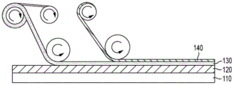
Fig. 2 is a diagram illustrating a manufacturing process of an adhesive film according to the present invention.
Fig. 3A to 3C are diagrams illustrating a process of treating a substrate using an adhesive film according to the present invention.
Fig. 4 is a cross-sectional view of an adhesive substrate according to the present invention.
Fig. 5A to 5C are diagrams illustrating a process of treating a substrate using an adhesive substrate according to the present invention.
Fig. 6 is a graph showing the heat resistance test results.
Fig. 7 is a graph showing the results of the adhesion property test.
Best mode
Various advantages and features of the present invention and methods of accomplishing the same will become apparent from the following description of exemplary embodiments with reference to the accompanying drawings. However, the present invention is not limited to the following exemplary embodiments, but may be implemented in various different forms. The exemplary embodiments are provided only to complete the present invention and to fully provide those skilled in the art with the scope of the present invention, which will be defined by the appended claims.
Shapes, sizes, ratios, angles, numbers, etc., shown in the drawings for describing exemplary embodiments of the present invention are only examples, and the present invention is not limited thereto. Like reference numerals refer to like elements throughout the specification. Further, in the following description, when it is determined that the gist of the present invention may be unnecessarily obscured, a detailed description of known related art will be omitted.
In this specification, when the terms "including", "having", and the like are used, other details than the above-described details may be added in addition to the use of the expression "only". Any reference to the singular may include the plural unless specifically stated otherwise.
Components are to be construed as including ordinary error ranges even if not explicitly stated.
When terms such as "upper", "above", "below", and "next" are used to describe a positional relationship between two parts, one or more parts may be located between the two parts unless these terms are used with the terms "immediately" or "directly".
The features of the exemplary embodiments of the present invention may be partially or completely connected or combined with each other, and various interlocking and driving may be technically performed.
Hereinafter, exemplary embodiments of the present invention will be described with reference to the accompanying drawings. The following exemplary embodiments will be provided as examples in order to fully convey the spirit of the present invention to those skilled in the art. Therefore, the present invention is not limited to the exemplary embodiments to be described below, and may be implemented in various different ways.
Fig. 1 is a cross-sectional view of an exemplary adhesive film according to an exemplary embodiment of the present invention. Referring to fig. 1, the adhesive film according to an exemplary embodiment of the present invention includes a first liner 110, an adhesive layer 120, a light-to-heat conversion layer 130, and a second liner 140 sequentially laminated.
The adhesive film of the present invention has a film shape, and may be configured by laminating the adhesive layer 120 formed in a film shape and the photothermal conversion layer 130 formed in a film shape. In a later process of treating the substrate to be treated, the adhesive layer 120 is adhered to the substrate to be treated, and the photothermal conversion layer 130 is adhered to the hard support.
More specifically, the photothermal conversion layer 130 is divided by irradiating radiant energy such as laser light so that the substrate or elements or circuits on the substrate can be separated from the support without being damaged.
The light-to-heat conversion layer 130 includes a light absorber and a thermally decomposable resin. Radiant energy applied to the light-to-heat conversion layer 130 in the form of, for example, laser light, is absorbed by the light absorber and converted into thermal energy. The generated thermal energy rapidly increases the temperature of the photothermal conversion layer 130, and the temperature reaches the thermal decomposition temperature of the thermally decomposable resin (organic component) in the photothermal conversion layer 130 to cause thermal decomposition of the resin. The gas generated by the thermal decomposition forms a void layer (such as a space) in the light-to-heat conversion layer 130, and the light-to-heat conversion layer 130 is divided into two parts to separate the support and the substrate from each other.
The light absorber can absorb radiant energy and convert the absorbed radiant energy into thermal energy. In addition, the light absorber serves to block light to prevent the substrate to be processed from being damaged by laser light or the like.
Although the light absorber varies depending on the wavelength of the laser light, examples of the light absorber that can be used include carbon black, graphite powder, particulate metal powder (e.g., iron, aluminum, copper, nickel, cobalt, manganese, chromium, zinc, and tellurium), metal oxide powder (e.g., black titanium oxide), and dyes and pigments (e.g., aromatic diamino-based metal complexes, aliphatic diamine-based metal complexes, aromatic dithiol-based metal complexes, hydroxythiophenol-based metal complexes, squarate-based compounds, cyanine-based dyes, methine-based dyes, naphthoquinone-based dyes, and anthraquinone-based dyes). The light absorber can be in the form of a film, including a vapor deposited metal film.
Among these light absorbers, carbon black is particularly useful, and because it significantly reduces the force required to separate the substrate from the support after irradiation and accelerates the separation.
The particle size of the light absorber in the light-to-heat conversion layer 130 may be about 20nm to about 2000nm, preferably about 50nm to about 1000nm, and more preferably about 100nm to about 350 nm. When the particle diameter of the light absorber is less than about 20nm, it is difficult to disperse the light absorber, and as the particle diameter becomes smaller, a large amount may not be loaded due to a high surface area and there is a limitation in the loading amount. Further, when the particle diameter of the light absorber exceeds about 2000nm, the laser blocking performance is lowered, and the splitting performance of the laser light to the photo-thermal conversion layer 130 is lowered. Further, as the particle diameter of the light absorber increases, the film forming property decreases, the dispersion stability after dispersion decreases, and the time until the liquid is prepared and coated needs to be shortened.
The light absorber is contained in the light-to-heat conversion layer 130 in an amount of about 5 wt% to about 80 wt%, preferably about 10 wt% to about 60 wt%, and more preferably about 20 wt% to about 50 wt%, based on the total weight of the light-to-heat conversion layer 130. When the content of the light absorber is less than about 5% by weight, separation by laser is difficult. In addition, when the content of the light absorber is more than about 80 wt%, a portion of the light-to-heat conversion layer 130 divided by the laser remains on the surface of the adhesive layer 120 after the light-to-heat conversion layer 130 is divided by the laser, and in this case, the adhesiveness is too low due to the high carbon content. In this case, in the process of removing the adhesive layer 120 by the removal tape later, there is a problem in that the adhesive layer 120 is difficult to remove because the adhesive layer 120 does not adhere well to the removal tape. In addition, as the content of the light absorber increases, the adhesion on the surface of the light-to-heat conversion layer 130 is too low, and thus it is difficult to laminate with the support and the dispersion of the light absorber is not uniform.
The thermally decomposable resin in the light-to-heat conversion layer 130 includes an acrylic resin. Preferably, the acrylic resin comprises monomers selected from the group consisting of: methyl Methacrylate (MMA), hydroxyethyl methacrylate (HEMA), Ethyl Acrylate (EA), Butyl Acrylate (BA), Acrylonitrile (AN), and combinations thereof. Preferably, the acrylic resin may be selected from a combination of three or more of the following: methyl Methacrylate (MMA), hydroxyethyl methacrylate (HEMA), Ethyl Acrylate (EA), Butyl Acrylate (BA), Acrylonitrile (AN). The acrylic resin may have a suitable molecular weight, Tg, heat resistance, and functional group.
The content of the acrylic resin may be about 5 to about 80 wt%, preferably about 15 to about 60 wt%, and more preferably about 40 to about 60 wt%, based on the total weight of the light-to-heat conversion layer 130. When the content of the acrylic resin is less than about 5 wt%, film formation is reduced, and it is difficult to adjust the thickness of the light-to-heat conversion layer 130, and the adhesion of the surface of the light-to-heat conversion layer 130 becomes too low and thus it is difficult to laminate with the support. Further, when the content of the acrylic resin is more than about 80% by weight, a physical force is required to partition the photothermal conversion layer 130 after laser irradiation, and it is difficult to separate the substrate from the support, and damage to the substrate to be processed and elements or circuits formed on the substrate may occur.
The acrylic resin preferably includes two acrylic resins having different weight average molecular weights, and more preferably has a high molecular weight acrylic resin and a low molecular weight acrylic resin. The high molecular weight acrylic resin allows the light-to-heat conversion layer 130 to have excellent heat resistance, and the low molecular weight acrylic resin serves to improve the adhesion of the light-to-heat conversion layer 130 and facilitate film formation.
At this time, the glass transition temperature Tg of the high molecular weight acrylic resin may be 0 ℃ to 10 ℃, and the Tg of the low molecular weight acrylic resin may be-10 ℃ to 0 ℃. When the Tg of the high molecular weight acrylic resin is higher than 10 ℃ and the Tg of the low molecular weight acrylic resin is higher than 0 ℃, the heat resistance of the light-to-heat conversion layer 130 may be improved, but the surface adhesion may be reduced. When the surface of the light-to-heat conversion layer 130 has low adhesion, release failure may occur when the adhesive layer 140 is peeled off using a removal tape. On the other hand, when the Tg of the high molecular weight acrylic resin is lower than 0 ℃ and the Tg of the low molecular weight acrylic resin is lower than-10 ℃, the adhesive property may be improved, but the heat resistance may be lowered.
The high molecular weight acrylic resin has a weight average molecular weight of from about 400,000g/mol to about 15,000,000g/mol, preferably from about 500,000g/mol to about 1,200,000g/mol, and more preferably from about 700,000g/mol to about 1,000,000 g/mol. When the weight average molecular weight of the high molecular weight acrylic resin is less than about 400,000g/mol, the heat resistance of the light-to-heat conversion layer 130 is deteriorated, and when the weight average molecular weight of the high molecular weight acrylic resin is more than about 15,000,000g/mol, it is not easy to coat the light-to-heat conversion layer 130 and mix the liquid.
The weight average molecular weight of the low molecular weight acrylic resin may be from about 50,000g/mol to about 600,000g/mol, preferably from about 100,000g/mol to about 500,000g/mol, and more preferably from about 400,000g/mol to about 500,000 g/mol. When the weight average molecular weight of the low molecular weight acrylic resin is less than about 50,000g/mol, the heat resistance of the light-to-heat conversion layer 130 is deteriorated, and when the weight average molecular weight of the low molecular weight acrylic resin is greater than about 600,000g/mol, the lamination performance of the light-to-heat conversion layer 130 is deteriorated.
The weight ratio of the low molecular weight acrylic resin to the high molecular weight acrylic resin may be from about 1:4 to about 4:1, preferably from about 1:3 to about 3:1, and more preferably from about 1:2 to about 2: 1. When the content of the low molecular weight acrylic resin is significantly less than that of the high molecular weight acrylic resin, the lamination property of the light-to-heat conversion layer 130 is deteriorated. In addition, when the content of the high molecular weight acrylic resin is significantly less than that of the low molecular weight acrylic resin, heat resistance of the photothermal conversion layer 130 is deteriorated and adhesion on the divided surfaces of the photothermal conversion layer 130 is strong after laser irradiation, and thus physically large force is required for separation.
The thermally decomposable resin has a functional group of-COOH or-OH. Preferably, the thermally decomposable resin comprises an acrylic resin having a-COOH or-OH functional group. The photothermal conversion layer 130 including the thermally decomposable resin having a functional group of-COOH or-OH is not a pressure sensitive adhesive type. The photothermal conversion layer 130 has a functional group of — COOH or — OH bonded to the support by hydrogen bonding, and may be hydrogen bonded to, for example, a silanol group on the glass surface of the support made of glass. In this case, the hydrogen bond provides initial adhesion for the adhesion between the adhesive layer and the support, and the adhesion between the light-to-heat conversion layer 130 and the support is greatly increased due to heat generated in a process after the bonding process.
The acid value of the-COOH or-OH functional group may be about 1mgKOH/g or more, preferably about 5mgKOH/g or more. The lamination property of the photothermal conversion layer 130 is based on the COOH or-OH functional group, and when the acid value of the COOH or-OH functional group is less than about 1mgKOH/g, the lamination property is deteriorated. The upper limit of the acid number of the COOH or-OH function is not a problem. However, due to the chemical structure, the acid value of the COOH or-OH functional group is preferably from about 1mgKOH/g to about 50mgKOH/g, more preferably from about 1mgKOH/g to about 30mgKOH/g, and most preferably from about 10mgKOH/g to about 20 mgKOH/g.
The light-to-heat conversion layer 130 may further include an inorganic filler. The inorganic filler plays a role of preventing re-adhesion of the light-to-heat conversion layer 130 after the light-to-heat conversion layer 130 is divided due to formation of a void layer caused by thermal decomposition of the thermally decomposable resin. Therefore, after processing the substrate, when the photothermal conversion layer 130 is divided by irradiating laser light, the physical force required to separate the substrate from the support may be further reduced.
The inorganic filler may be selected from SiO2、Al2O3、TiO2And combinations thereof. In particular, in TiO2In the case of (2), there is an additional light-shielding effect on the substrate to be treated.
The particle size of the inorganic filler in the light-to-heat conversion layer 130 may be about 20nm to about 2000nm, preferably about 50nm to about 1000nm, and more preferably about 100nm to about 350 nm. When the particle diameter of the inorganic filler is less than about 20nm, the dispersion of the inorganic filler is not easy in manufacturing a film, and there is a limit to the amount of the inorganic filler to be loaded. Also, when the particle diameter of the inorganic filler is greater than about 2000nm, the film forming property is lowered and dispersion durability after dispersion is deteriorated.
The content of the inorganic filler in the light-to-heat conversion layer 130 may be about 4 wt% to about 60 wt%, preferably about 5 wt% to about 50 wt%, and more preferably about 5 wt% to about 30 wt%, based on the total weight of the light-to-heat conversion layer 130. When the content of the inorganic filler is less than about 4 wt%, the photothermal conversion layer 130 may be re-bonded again with the lapse of time because the adhesion of the separation surface is great after the separation process by laser irradiation. Further, when the content of the inorganic filler is more than about 60 wt%, the adhesion of the light-to-heat conversion layer 130 is too low, and thus it is difficult to laminate the light-to-heat conversion layer 130 on the support, the film forming property is reduced, and the dispersion is not uniform.
The light-to-heat conversion layer 130 may further include a dispersant. The content of the dispersant may be about 0.1 wt% to about 10 wt%, preferably about 0.1 wt% to about 7 wt%, and more preferably about 0.1 wt% to about 5 wt%, based on the total weight of the light-to-heat conversion layer 130. When the content of the dispersing agent is less than about 0.1 wt%, the dispersibility of the light absorber and the inorganic filler in the light-to-heat conversion layer 130 may be deteriorated, and the dispersion durability after dispersion may also be reduced. In addition, when the content of the dispersant is more than about 10 wt%, the heat resistance of the light-to-heat conversion layer 130 is deteriorated, the added additive is decomposed at high temperature and the weight loss increases.
The light-to-heat conversion layer 130 may be formed in a film shape as follows. A light absorber such as carbon black is added to a solvent such as Methyl Ethyl Ketone (MEK) or Ethyl Acetate (EA), and at this time, a dispersant and an inorganic filler may be added together and then dispersed by ultrasonic treatment. Two acrylic resins having different weight average molecular weights were stirred at room temperature for 30 minutes by a stirrer, and then a solution in which a light absorbing agent was dispersed was added to the stirred mixture, and the mixture was stirred again under the same conditions. Thereafter, a solvent is added to adjust viscosity and solid content to a favorable coating state, and the solvent is coated on peeled polyethylene terephthalate (PET) having an appropriate thickness by a coater having a comma-shaped roll head, a slot die, or a lip die, and then dried at a temperature of about 90 ℃ to about 130 ℃ for 2 minutes or more to form a film-type photothermal conversion layer.
The thickness of the light-to-heat conversion layer 130 is about 1 μm to about 15 μm, preferably about 2 μm to about 10 μm, and more preferably about 3 μm to about 6 μm. When the thickness of the light-to-heat conversion layer 130 is less than about 1 μm, a portion of the adhesive layer 120 may remain on the substrate to be treated during the separation of the light-to-heat conversion layer 130, and the laser blocking property of the light absorber may be deteriorated. Further, when the thickness of the light-to-heat conversion layer 130 exceeds about 15 μm, a physically large force is required to separate the light-to-heat conversion layer 130 after laser irradiation.
Such a photothermal conversion layer 130 is formed in a film shape. When the photothermal conversion layer 130 is directly coated on the support in a liquid form, the viscosity is low, the thickness is less than about 1 μm, and the thickness may not be formed to be sufficiently large. Therefore, it is difficult to sufficiently use a light absorber capable of blocking laser light, and to prevent damage of the laser light to the substrate to be processed. The photothermal conversion layer 130 according to the present invention is formed in a film shape, and thus its thickness is easily adjusted, and it is more advantageous to protect a substrate to be processed and a circuit or an element formed thereon. In addition, the adhesion of such a photothermal conversion layer 130 to a support may be 150gf/25mm to 1600gf/25 mm.
The adhesive layer 120 serves to fix the substrate to be treated to the support through the light-to-heat conversion layer 130. The adhesive layer 120 may be formed to directly contact the light-to-heat conversion layer 130.
After the substrate and the support are separated by the decomposition of the photothermal conversion layer 130, the substrate having the adhesive layer 120 thereon is obtained. Therefore, the adhesive layer 120 needs to be easily separated from the base by peeling or the like, and the adhesive strength of the adhesive layer 120 is high enough to fix the base sheet on the support but low enough to be separated from the base sheet. Such an adhesive layer 120 has a film shape and is not a photo-curing adhesive.
The adhesive layer 120 may be an acrylic adhesive layer. Preferably, the adhesive layer 120 may include 2-ethylhexanol (2-EHA), Acrylic Acid (AA), Glycidyl Methacrylate (GMA), and an isocyanate-based curing agent. In this case, the isocyanate-based curing agent may include a curing agent selected from the group consisting of: toluene Diisocyanate (TDI), methylene diphenyl diisocyanate (MDI), Hexamethylene Diisocyanate (HDI), isophorone diisocyanate (IPDI), Xylene Diisocyanate (XDI), and combinations thereof.
The adhesive layer 120 has a thickness of about 5 μm to about 100 μm, preferably about 5 μm to about 70 μm, and more preferably about 10 μm to about 60 μm. When the thickness of the adhesive layer 120 is less than about 5 μm, delamination may occur due to low adhesion when deformation of the device is severe. In addition, when the adhesive layer 120 is removed after finishing the treatment of the substrate to be treated, the adhesive layer may be torn and residues may remain. In addition, when the thickness of the adhesive layer 120 is greater than about 100 μm, the solvent may remain because the drying efficiency is reduced when the adhesive layer 120 is formed, and the cohesive force of the adhesive layer 120 may be reduced and thus the residue may remain.
The first and second spacers 110 and 140 serve to support and protect the adhesive layer 120 and the light-to-heat conversion layer 130, respectively. When the adhesive film is used, the first liner 110 and the second liner 140 are removed.
The first and second spacers 110 and 140 may be silicon-coated polyethylene terephthalate (PET), but are not limited thereto, and any material capable of supporting and protecting the adhesive layer 120 and the light-to-heat conversion layer 130 is sufficient.
Fig. 2 is a diagram illustrating a manufacturing process of an adhesive film according to an exemplary embodiment of the present invention. Referring to fig. 2, the film-shaped photothermal conversion layer 130 is laminated on the film-shaped adhesive layer 120 formed on the first liner 110 by a roll-to-roll method. Thereafter, similarly, the second gasket 140 may be laminated on the photothermal conversion layer 130 by a roll-to-roll method.
However, the method of manufacturing the adhesive film of the present invention is not limited thereto, and any method of laminating the film-shaped adhesive layer 120 and the film-shaped photothermal conversion layer 130 in contact with each other is sufficient.
In the case of using a liquid adhesive material and a liquid photothermal conversion material between a substrate to be treated and a support, a process for forming a photothermal conversion layer by applying and curing the photothermal conversion material on the support and a process for forming an adhesive layer by applying and curing an adhesive material on the substrate to be treated are required, respectively. Thereafter, a process of bonding the adhesive layer and the photothermal conversion layer in a vacuum is required. That is, when a liquid material is used, coating time, curing time, and bonding time are required.
On the other hand, in the case of using the film-type adhesive film according to the present invention, a process of removing the first liner, attaching the adhesive layer to the substrate to be treated, removing the second liner, and attaching the photothermal conversion layer to the support is sufficient. Therefore, the present invention can significantly reduce the required process time and reduce the cost required for a coating process, a curing process, a vacuum process, etc.
Fig. 3A to 3C are diagrams illustrating a process of treating a substrate using an adhesive film according to the present invention.
Referring to fig. 3A, in the adhesive film of the present invention, the second gasket is removed, the light-to-heat conversion layer 130 is attached to the support 300, the first gasket is removed, and the adhesive layer 120 is attached to the substrate to be treated 200. In this case, the process is preferably performed at about 40 ℃ to about 80 ℃, so that the adhesion between the light-to-heat conversion layer 130 and the support 300 is increased.
The carrier 300 is a material capable of transmitting radiant energy, such as a laser used in the present invention, and is required to maintain the substrate to be processed 200 in a flat state and prevent the substrate to be processed 200 from being damaged during processing and transportation. The carrier 300 is preferably rigid and transmissive.
The transmittance of the support 300 is not limited unless it prevents radiant energy from being transmitted into the light-to-heat conversion layer 130 so as to enable decomposition of the light-to-heat conversion layer 130. However, the transmittance may be, for example, about 50% or more.
In order to prevent the substrate to be treated from being deformed during the treatment, it is preferable that the carrier 300 has a sufficiently high rigidity, and the bending strength of the carrier 300 is preferably 2 × 10⁻³(Pa·m3) Or larger, and more preferably 3 × 10⁻²(Pa·m3) Or larger.
Further, it is preferable that the carrier 300 has sufficient heat resistance to prevent damage due to heat history that may occur during the process performed on the substrate to be treated, and the heat distortion temperature of the carrier 300 is preferably 550 ℃ or more, or more preferably 700 ℃ or more.
The carrier 300 may be, for example, glass. In addition, in order to improve adhesive strength with an adjacent layer such as the light-to-heat conversion layer 130, the support 300 may be surface-treated with a binder or the like, if necessary.
Thereafter, the substrate to be treated 200 and the support 300 are fixed to each other with the adhesive film including the photothermal conversion layer 130 and the adhesive layer 120 interposed therebetween, and then the substrate to be treated 200 is treated.
The substrate to be processed 200 is a substrate fixed and processed to the carrier 300 and then separated from the carrier 300, and may be, for example, a wafer or a substrate for a flexible display.
As an example, the substrate to be processed 200 may include a semiconductor wafer such as silicon and gallium arsenide, a quartz wafer, sapphire, or glass. The circuit surface of the substrate to be treated 200 may be adhered to the adhesive layer 120. Thereafter, the surface of the substrate to be treated 200, which is not adhered to the adhesive layer 120, may be ground by a grinder or the like to be processed into a thin substrate.
As another example, the substrate to be processed 200 may be an epoxy molded wafer. The molding surface of the substrate to be processed 200 may be adhered to the adhesive layer 120, and thereafter, the substrate to be processed 200 may be processed into a complete substrate by performing a predetermined process for connecting a circuit to the surface of the substrate to be processed 200, which is not adhered to the adhesive layer 120.
Meanwhile, as yet another example, the substrate to be processed 200 may be a plastic substrate, a metal thin film, or the like as a flexible substrate. For example, the substrate to be treated 200 may be PI. However, the substrate to be processed 200 is not limited thereto, and as a material having a flexible property, a material that can be used as a substrate of a flexible display is sufficient.
For example, "processing" may include a process of forming an element layer on the substrate to be processed 200. Although not shown, the element layer may be composed of a plurality of thin film layers and an electric element, and more particularly, the element layer may include a thin film transistor including a gate electrode, a semiconductor layer, a source electrode, and a drain electrode.
The flexible display may be any one selected from an organic light emitting diode display, a liquid crystal display, and an electrophoretic display. However, the present invention is not limited thereto, and the flexible display may include all flexible displays using a flexible substrate.
Referring to fig. 3B, after a desired processing level, separation of the carrier 300 and the processed substrate 210 is performed by irradiating the laser 400. The laser light 400 is irradiated from the carrier 300 side.
The light absorber of the light-to-heat conversion layer 130 absorbs radiant energy by the laser 400 to convert the radiant energy into thermal energy. The generated thermal energy rapidly increases the temperature of the light-to-heat conversion layer 130, and the temperature causes decomposition of the thermally decomposable resin in the light-to-heat conversion layer 130. The gas generated by the thermal decomposition forms a void layer in the light-to-heat conversion layer 130, and the light-to-heat conversion layer 130 is divided into two parts to separate the support 300 and the treated substrate 210 from each other.
The thermally decomposable resin in the light-heat conversion layer 130 is decomposed by irradiation of the laser light 400 to form cracks inside the layer, thereby separating the light-heat conversion layer itself. The gas generated by the decomposition of the resin is eventually introduced between the two layers to separate the two layers from each other. Therefore, in order to facilitate the introduction of the gas, it is preferable to irradiate the laser light 400 into the light-to-heat conversion layer 130 from the edge portion of the light-to-heat conversion layer 130.
In order to use the laser light 400 from the edge portion of the photothermal conversion layer 130, a method of applying the laser light 400 while linearly reciprocating from the edge portion, or alternatively, a method of spirally irradiating the laser light 400 from the edge portion toward the center like a phonograph may be used.
The laser light 400 is generally a laser light having a wavelength of about 300 to about 11,000nm and preferably about 300 to about 2,000nm, and the laser light 400 includes, as specific examples, a YAG laser light emitting light having a wavelength of 1064nm, a second-harmonic generation YAG laser light having a wavelength of 532nm, and a semiconductor laser light having a wavelength of 780 to 1,300 nm.
Referring to fig. 3C, after removing the carrier 300, the adhesive layer 120 on the processed substrate 210 is removed. In order to remove the adhesive layer 120, it is preferable to use a removal tape 500 having stronger adhesiveness to the adhesive layer 120 than the adhesiveness between the treated substrate 210 and the adhesive layer 120. Such a removal tape 500 may be adhered to the adhesive layer 120 and then peeled off together with the adhesive layer 120 to remove the adhesive layer 120 from the treated substrate 210. Although not shown in the drawings, a portion of the light-to-heat conversion layer 130 may remain after the light-to-heat conversion layer 130 is divided on the adhesive layer 120.
Meanwhile, although not shown in the drawings, after removing the carrier 300, the adhesive layer 120 on the handle substrate 210 may be removed using a removing solution. Preferably, the adhesive layer 120 in which a portion of the photothermal conversion layer remains may be immersed in a removing solution to remove the adhesive layer 120. Preferably, the adhesive layer 120 may be immersed in the removal solution for about 10 seconds to 60 seconds. In addition, the removal solution may include trans-1, 2-dichloroethylene and a hydrofluoroether.
When the size or area of the processed substrate 210 is relatively large, it may be difficult to remove the adhesive layer 120 with the removal tape 500 at one time. However, when the removing solution is used, it is advantageous to remove the adhesive layer 120 having a large area. In addition, additional external physical force is not required, and the adhesive layer 120 can be removed in a short time without residue.
The method of treating a substrate according to the present invention is environmentally friendly because a solvent is not required when treating a substrate by using a previously prepared adhesive film. Further, in the case of using a previously prepared adhesive film, exposure of the support and the substrate to heat, UV, or the like can be reduced when the substrate is treated, thereby preventing additional damage.
Further, since a process of directly coating and curing the adhesive material or the photothermal conversion material on the support or the substrate to be treated can be omitted, the process can be simplified, and the processing cost and time can be reduced. Further, it is advantageous to form the adhesive layer and the photothermal conversion layer in a uniform thickness, and the process can be used even in the treatment of a large-area substrate.
Next, an adhesive substrate according to the present invention will be described with reference to fig. 4. The duplicated description of the above adhesive film may be omitted, and like reference numerals denote like constituent elements. Fig. 4 is a cross-sectional view of an adhesive substrate according to the present invention.
Referring to fig. 4, the adhesive substrate according to an exemplary embodiment of the present invention includes a gasket 150, a light-to-heat conversion layer 130, an adhesive layer 120, and a substrate to be treated 600, which are sequentially laminated. The adhesive layer 120 and the light-to-heat conversion layer 130 may be laminated on the substrate 600 to be treated. The photothermal conversion layer 130 adheres to the hard support during the processing of the substrate 600 to be processed later.
The adhesive layer 120 and the light-to-heat conversion layer 130 of the adhesive substrate are the same as those of the adhesive film described above. That is, the adhesive substrate according to the present invention may include the above adhesive film and a substrate to be treated. However, the spacer 150 may be provided only on the light-to-heat conversion layer 130 in the adhesive substrate.
The substrate to be processed 600 may be a substrate for a flexible display.
For example, the substrate to be processed 600 may be used as a plastic substrate, a metal thin film, or the like as a flexible substrate. However, the substrate 600 to be processed is not limited thereto, and as a material having a flexible property, a material that can be used as a substrate of a flexible display is sufficient. Preferably, the substrate 600 to be treated may be a PI film.
The substrate 600 to be processed may be processed into a substrate on which an element layer is formed. The element layer may be composed of a plurality of thin film layers and an electric element, and more specifically, the element layer may include a thin film transistor including a gate electrode, a semiconductor layer, a source electrode, and a drain electrode. For example, a thin film transistor and an organic layer are formed on the substrate 600 to be processed, and an encapsulation layer is formed on the thin film transistor and the organic layer to manufacture a processed substrate.
The flexible display may be any one selected from an organic light emitting diode display, a liquid crystal display, and an electrophoretic display. However, the present invention is not limited thereto, and the flexible display may include all flexible displays using a flexible substrate.
The gasket 150 serves to support and protect the light-to-heat conversion layer 130. When the light-to-heat conversion layer 130 is attached to the support to process the substrate 600 to be processed, the liner 150 is removed. The spacer 150 may be silicone-coated polyethylene terephthalate (PET), but is not limited thereto, and a material capable of supporting and protecting the light-to-heat conversion layer 130 is sufficient.
The thin film type light-to-heat conversion layer 130 is laminated on the thin film type adhesive layer 120 formed on the substrate 600 to be processed by a roll-to-roll method, and then, the gasket 150 may be laminated on the light-to-heat conversion layer 130 in the same manner by a roll-to-roll method to form an adhesive substrate.
However, the manufacturing process of the adhesive substrate of the present invention is not limited thereto, and any method of laminating the adhesive layer 120 and the film-type photothermal conversion layer 130 on the substrate 600 to be treated so as to be in contact with each other is sufficient.
The adhesive substrate of the present invention uses the film-type photothermal conversion layer 130, thereby significantly reducing the required process time, and reducing the cost and the like required for the application process, the curing process, the vacuum process, and the like, as compared to the case of using a liquid material. In addition, since the adhesive substrate of the present invention includes the substrate to be treated 600, a step of adhering an adhesive film to the substrate to be treated during the treatment of the substrate is omitted, thereby simplifying the process and reducing time and cost.
Fig. 5A to 5C are diagrams illustrating a process of treating a substrate using an adhesive substrate according to the present invention.
Referring to fig. 5A, in the adhesive substrate according to the present invention, the gasket is removed and the light-to-heat conversion layer 130 is attached to the support 300. In this case, the process is preferably performed at about 40 ℃ to about 80 ℃, so that the adhesion between the light-to-heat conversion layer 130 and the support 300 is increased.
The carrier 300 is a material capable of transmitting radiant energy, such as a laser used in the present invention, and is required to maintain the substrate 600 to be processed in a flat state and prevent the substrate 600 to be processed from being damaged during processing and transportation. The carrier 300 is preferably rigid and transmissive.
The transmittance of the support 300 is not limited unless it prevents radiant energy from being transmitted into the light-to-heat conversion layer 130 so as to enable decomposition of the light-to-heat conversion layer 130. However, the transmittance may be, for example, about 50% or more.
Furthermore, in order to prevent the substrate to be treated from being deformed during the treatmentIt is preferable that the carrier 300 has a sufficiently high rigidity and the bending strength of the carrier 300 is preferably 2 × 10⁻³(Pa·m3) Or larger, and more preferably 3 × 10⁻²(Pa·m3) Or larger.
Further, it is preferable that the carrier 300 has sufficient heat resistance to prevent damage due to heat history that may occur during the process performed on the substrate to be treated, and the heat distortion temperature of the carrier 300 is preferably 550 ℃ or more, or more preferably 700 ℃ or more.
The carrier 300 may be, for example, glass. In addition, in order to improve adhesive strength with an adjacent layer such as the light-to-heat conversion layer 130, the support 300 may be surface-treated with a binder or the like, if necessary.
Thereafter, the substrate 600 to be treated and the support 300 are fixed to each other with the adhesive film including the photothermal conversion layer 130 and the adhesive layer 120 interposed therebetween, and then the substrate 600 to be treated is treated. The substrate 600 to be processed is a substrate that is fixed and processed to the carrier 300 and then separated from the carrier 300.
The substrate to be processed 600 is a substrate for a flexible display, and may be processed into a substrate having an element layer formed on the substrate to be processed 600.
Referring to fig. 5B, after a desired processing level, separation of the carrier 300 and the processed substrate 610 is performed by irradiating the laser 400. The laser light 400 is irradiated from the carrier 300 side.
The light absorber of the light-to-heat conversion layer 130 absorbs radiant energy by the laser 400 to convert the radiant energy into thermal energy. The generated thermal energy rapidly increases the temperature of the light-to-heat conversion layer 130, and the temperature causes decomposition of the thermally decomposable resin in the light-to-heat conversion layer 130. The gas generated by the thermal decomposition forms a void layer in the light-to-heat conversion layer 130, and the light-to-heat conversion layer 130 is divided into two parts to separate the support 300 and the treated substrate 610 from each other.
The thermally decomposable resin in the light-heat conversion layer 130 is decomposed by irradiation of the laser light 400 to form cracks inside the layer, thereby separating the light-heat conversion layer itself. The gas generated by the decomposition of the resin is eventually introduced between the two layers to separate the two layers from each other. Therefore, in order to facilitate the introduction of the gas, it is preferable to irradiate the laser light 400 into the light-to-heat conversion layer 130 from the edge portion of the light-to-heat conversion layer 130.
In order to use the laser light 400 from the edge portion of the photothermal conversion layer 130, a method of applying the laser light 400 while linearly reciprocating from the edge portion or, alternatively, a method of spirally irradiating the laser light 400 from the edge portion toward the center like a phonograph may also be used.
The laser light 400 is generally a laser light having a wavelength of about 300 to about 11,000nm and preferably about 300 to about 2,000nm, and the laser light 400 includes, as specific examples, a YAG laser light emitting light having a wavelength of 1064nm, a second-harmonic generation YAG laser light having a wavelength of 532nm, and a semiconductor laser light having a wavelength of 780 to 1,300 nm.
Referring to fig. 5C, after removing the carrier 300, the adhesive layer 120 on the processed substrate 610 is removed. The adhesive layer 120 may be removed using a removal solution 700. Although not shown to be removed in the drawings, a portion of the photothermal conversion layer may remain after the photothermal conversion layer is divided on the adhesive layer 120. The adhesive layer 120 in which a portion of the photothermal conversion layer remains may be immersed in the removal solution 700 to remove the adhesive layer 120.
Preferably, the adhesive layer 120 may be removed by immersing the adhesive layer 120 in the removing solution 700 contained in the container 800 for about 10 seconds to 60 seconds. Such a removal solution 700 may include trans-1, 2-dichloroethylene and a hydrofluoroether.
In particular, when the processed substrate 610 has a large size or area, or when the processed substrate 610 is made of a thin and brittle material, it is advantageous to use the removing solution 700 when removing the adhesive layer 120. The use of the removing solution 700 does not require additional external physical force and can remove the adhesive layer 120 without residue in a short time.
Meanwhile, although not shown in the drawings, in order to remove the adhesive layer 120, a removal tape having stronger adhesiveness to the adhesive layer 120 than that between the treated substrate 610 and the adhesive layer 120 may also be used. When the size or area of the adhesive layer 120 or the treated substrate 610 is small, the adhesive layer 120 can be easily removed by using such a removal tape.
The method of treating a substrate according to the present invention is environmentally friendly and can prevent additional damage to the substrate. Furthermore, the process is simplified, thereby reducing processing costs and time.
Hereinafter, the present invention will be described in more detail by experimental examples, but the following experimental examples are only for verifying the present invention and the present invention is not limited thereto. That is, the embodiments of the present invention may be modified into various forms, and the scope of the present invention should not be construed as being limited by the experimental embodiments described below.
Example 1
6 wt% of carbon black (Cancarb Corporation) having a particle size of 240nm, 4 wt% of titanium dioxide (Huntsman) having a particle size of 240nm, and 1 wt% of a dispersant (BYK Chemie Japan Co., Ltd.) were added to 75 wt% of methyl ethyl ketone (MEK, Samchun Chemical Co., Ltd.) and dispersed by using an ultrasonic disperser for 30 minutes to prepare a solution in which a light absorbing agent was dispersed. 7% by weight of a high molecular weight acrylic polymer elastomer other than PSA having a weight average molecular weight of 1,000,000g/mol and a COOH/OH functional group of 10mgKOH/g or more, and 7% by weight of a low molecular weight acrylic polymer elastomer other than PSA having a weight average molecular weight of 500,000g/mol and a COOH/OH functional group of 5mgKOH/g or more, were mixed with each other and stirred with a stirrer for 30 minutes to prepare a thermally decomposable resin. The thermally decomposable resin is added to the solution in which the light absorbing agent is dispersed, and then stirred for another 20 minutes. Thereafter, Methyl Ethyl Ketone (MEK) is added so that the mixture has a viscosity suitable for coating of 200CPS to 5,000 CPS. The completed mixture was coated on a peeled polyethylene terephthalate (PET) (SG-31) having a thickness of 5 μm by a coater having a comma-shaped roll head, and then dried at a temperature of 110 to 130 ℃ for 2 minutes to form a film-type photothermal conversion layer.
The photothermal conversion layer prepared by this method includes 24 wt% of carbon black, 16 wt% of titanium dioxide, 4 wt% of a dispersant, 28 wt% of a high molecular weight acrylic polymer elastomer, and 28 wt% of a low molecular weight acrylic polymer elastomer, based on the total weight of the photothermal conversion layer.
The adhesive layer (3M company, ATT4025) formed on the previously prepared first gasket and the photothermal conversion layer formed on the second gasket were laminated through a roll-to-roll process to prepare a final adhesive film.
Thereafter, the second liner is first removed to bond the support to the photothermal conversion layer, and then the first liner is removed to bond the substrate to be treated and the adhesive layer, so that a laminate of a glass plate, an adhesive film, and a wafer is formed. The lamination of the adhesive film to the support and the substrate to be treated took about 3 minutes and all the bonding process was carried out on a hot plate at 70 ℃.
A circular glass plate (Corning) of 203mm (diameter) × 0.7mm was used as a transmission carrier, and a circular silicon wafer of 203mm (diameter) × 750 μm (thickness) was used as a substrate to be treated.
Thereafter, the laminate of the glass plate, the adhesive film and the wafer was placed on a grinding apparatus, and grinding was performed by bringing a rotating grinding wheel into contact with the laminate while supplying water. Grinding was performed to provide a wafer thickness of 50 μm.
After completion of the polishing, laser irradiation was performed using a YAG laser (wavelength: 1,064nm) having a laser output of 15W, a laser diameter and a scanning pitch of 100 μm, and a laser irradiation speed of 1.0 m/s. The laser light is irradiated onto the laminate and the entire surface of the laminate by linearly reciprocating in a tangential direction from the edge portion of the laminate. Thereafter, the glass plate is easily separated from the ground wafer, and a wafer having an adhesive layer is obtained thereon.
To release the adhesive layer from the wafer, a pressure-sensitive removal tape (3M; SCOTCH)TM#3305) was attached to the surface of the adhesive layer at a temperature of 40 ℃ and peeled off in the 180 ° direction, so as to obtain a silicon wafer having a thickness of 50 μm without wafer damage.
Examples 2 to 8
Laminated films including film-type photothermal conversion layers according to examples 2 to 8 were prepared in the same manner as in example 1, except for the contents of the respective components. The component contents of the photothermal conversion layer in each example are shown in table 1 below.
[ Table 1]


Subsequently, the support and the photothermal conversion layer are bonded to each other and the substrate to be treated and the adhesive layer are bonded to each other to form a laminate of a glass plate, an adhesive film and a wafer. Thereafter, in the same manner as in example 1, lapping of the wafer was performed, and laser light was irradiated onto the laminate to separate the carrier. Thereafter, the adhesive layer was peeled off using a pressure-sensitive removal tape. This process was performed in the same manner as in example 1.
In the laminates according to examples 2 to 8, when the glass plate is easily separated from the ground wafer, the carrier can be easily separated, and the wafer having the adhesive layer thereon can be obtained without being damaged. In addition, in the case of peeling the adhesive layer with a removal tape, it was confirmed that the wafer was not damaged.
Comparative example 1
A liquid photothermal conversion material (3M LTHC ink) was coated on a support (dow corning glass (8 inches)) by spin coating. After coating, the photothermal conversion material was thermally cured at a temperature of 150 ℃ to 180 ℃ for 2 hours to prepare a support coated with the photothermal conversion material having a thickness of about 0.9 μm.
The adhesive material (3M; LC-5320) was coated on the substrate to be treated (bare mirror wafer, 8 inches, 750 μ M) by spin coating. The amount of binder material required for one application is at least 2g and at most 10 g. Spin coating is achieved by adjusting the spin speed in two steps, and rotating at 500RPM in the first step and 1200 RPM in the second stepThe RPM rotates. Forming an adhesive layer by spin coating on a substrate to be treated, and then at 10-5To 10-9(Torr) the support coated with the photothermal conversion material and the substrate to be treated coated with the bonding material were bonded to each other under vacuum. Thereafter, the intensity was 1200mJ/cm2The adhesive material is irradiated with UV and photo-cured to prepare a substrate to be treated coated with the adhesive material.
It took about 125 minutes to prepare a laminate by forming the photothermal conversion material and the bonding material between the support and the substrate to be treated.
Comparative example 2
The experiment was performed in the same manner as in example except that, in a state where an adhesive having lower adhesiveness than that of the wafer was in contact with the wafer without using any photothermal conversion layer, a double-sided pressure sensitive removal tape (SCOTCH) was usedTM#9415 high adhesion/low adhesion) instead of the adhesive layer, a laminate composed of a silicon wafer, a pressure-sensitive removal tape, and a glass substrate was prepared. The silicon wafer cannot be peeled off.
Experimental example 1 Heat resistance test
The heat resistance of the film samples in example 1, examples 6 to 8, and comparative example 1 was evaluated using a thermogravimetric analyzer (TGA). 10mg of each sample was divided and the weight loss of the sample was measured under a nitrogen atmosphere at specific temperatures (200 ℃ and 250 ℃) and over a period of time (1 hour). The results are shown in table 2 below.
[ Table 2 ]]

Referring to table 2 above, similar weight loss was observed at 200 ℃ in the examples and comparative example 1, but the weight loss was significantly different at 250 ℃. Therefore, it can be confirmed that example 1 and examples 6 to 8 have more excellent heat resistance than comparative example 1.
Further, the laminate prepared according to example 1 and the laminate prepared according to comparative example 1 were aged at 300 ℃ for 1 hour in a nitrogen atmosphere, respectively. Results referring to fig. 6, after the bonding process, neither the laminate prepared according to comparative example 1 at room temperature nor the laminate prepared according to example 1 was damaged, but after aging at 300 ℃ for 1 hour, it was visually confirmed that damage occurred in the laminate prepared according to comparative example 1.
Therefore, it was confirmed that the embodiment using the film-type adhesive film has excellent heat resistance as in the present invention.
Experimental example 2 shadingPropertiesTest of
To evaluate the light-shielding property, the film samples in examples 1 to 5 and comparative example 1 were laminated between two glass slides. The prepared laminate was placed in a sensor portion of a laser pointer (NOVA II from OPHIR Photonics Corporation), and then irradiated with a laser at a laser output of 20W using a YAG laser (SS16-716, wavelength: 1,064nm, laser diameter: 0.4mm, frequency: 25KHz, irradiation speed: 1100mm/s, caliber: 0.05 mm).
Therefore, the laminates prepared according to comparative example 1 had a light transmittance of 19% measured by light of 3.7W, and the laminates prepared according to examples 1 to 5 had a light transmittance of 1% measured by light of 0.2W, respectively.
Therefore, it can be confirmed that the light-shielding effect of the example using the film-type adhesive film is more excellent than that of comparative example 1 like the present invention.
EXAMPLE 3 adhesion test
After the photothermal conversion layers of the adhesive films according to examples 2 to 5 were bonded to the glass plate, the adhesion between the glass plate and the photothermal conversion layer was measured after bonding and after aging at 220 ℃ for 1 hour, respectively.
Further, after the adhesive layer of the adhesive film according to examples 2 to 5 was bonded to the wafer, the adhesiveness between the wafer and the adhesive layer after bonding and after aging at 220 ℃ for 1 hour was measured, respectively.
The results are shown in table 3 below.
[ Table 3]

2000gf/25mm refers to the adhesiveness between the removal tape for peeling off the adhesive film and the adhesive film. Since the adhesive film is soft, the adhesiveness cannot be measured by directly stretching the adhesive film, and the adhesiveness is measured when another substrate is bonded and peeled on the upper portion of the adhesive film. At this time, since the adhesiveness between the adhesive film and the glass plate was too high, the adhesive film was not separated, and when another substrate (removal tape) bonded to the upper portion and the adhesive film were separated from each other, 2000gf/25mm was measured. Therefore, it is expected that the adhesion between the adhesive film and the glass plate is actually more than 2000gf/25 mm.
Referring to table 3, example 2, in which the acrylic resin content was high, had the highest adhesion after bonding. However, it was confirmed that when the heat treatment was performed, the adhesion was high in all the examples, and the adhesive film and the glass plate were not separated from each other before the laser irradiation, and the adhesion between the glass plate and the adhesive film was excellent during the process.
Meanwhile, the initial adhesion between the adhesive layer and the wafer was 400gf/25mm or more, but was reduced to about 180gf/25mm upon application of constant heat. Therefore, the adhesive film and the wafer are easily peeled off after the treatment due to the decrease in adhesiveness by heat, and a residue may not be left.
Experimental example 4 optimization of the content of carbon Black and acrylic resin
Laminate films according to examples 9 to 27 were prepared in the same manner as in example 1 except for the contents of the respective components. In addition, in examples 25 to 27, alumina (Denka) was used instead of titanium dioxide. In examples 9 to 27, all the film-type photothermal conversion layers can be formed, and a laminated film including the photothermal conversion layer can be prepared.
Next, the adhesive property of the laminated films according to examples 9 to 27, the debonding property after laser irradiation, and the peeling property of the glass plate of the photothermal conversion layer were tested.
When the prepared adhesive film was adhered to a glass plate having a width of 1 inch at 70 ℃ using a roll, a bonding performance test was performed, PET was attached to the adhesive film bonded to the glass plate, and then the adhesive film containing PET was peeled from the glass plate using UTM and the adhesiveness was measured (peeling speed: 300mm/min, peeling angle: 180), and the bonded state was observed with the naked eye. The results were classified according to the following criteria.
Very good: good adhesion to the front surface of the glass sheet,
Δ: voids were observed over the entire surface of the glass sheet,
x: the bond does not perform partially or completely well.
When the prepared adhesive film was bonded to a glass plate at 70 ℃, a debonding performance test after laser irradiation was performed, and then the glass plate bonded to the adhesive film was bonded to a wafer again at 40 ℃, and thereafter, debonding was performed by laser irradiation to confirm debonding. The results were classified according to the following criteria.
Very good: can be easily removed without any external stimulus
O: it is necessary to apply weak force to separate the photothermal conversion layer and the glass plate,
Δ: debonding by applying strength and lift (without workability)
X: without debonding (without processability)
The peel performance test was carried out when the glass plate was debonded after laser irradiation, using a pressure-sensitive removal tape (3M; SCOTCH) at 40 ℃TM#3305) the adhesive layer left on the wafer was removed, and then the residue was inspected with the naked eye. The results were classified according to the following criteria.
Very good: can be removed without any residue
O: a small amount of residue was found along the edges of the glass sheet,
Δ: a small amount of residue was found outside the edge,
x: there are many parts that do not peel integrally.
The component contents of the photothermal conversion layer and the experimental results in each example are shown in table 4 below, and each value represents wt%.
[ Table 4 ]]

Referring to table 4, in examples 9 to 27, the film-type photothermal conversion layer may be formed. Specifically, it was confirmed that when the content of the acrylic resin (sum of the contents of the high molecular weight acrylic polymer elastomer and the low molecular weight acrylic polymer elastomer) was 40% by weight or more and the total content of the filler (sum of the contents of carbon black, titanium dioxide and alumina) was 60% by weight or less, the adhesive property, the peeling property and the like were excellent.
Experimental example 5 optimization of acrylic resin
A laminated film including the film-type photothermal conversion layers according to comparative examples 3 and 4 and example 28 was prepared in the same manner as in example 1, except for the contents of the respective components. The component contents of the photothermal conversion layer in comparative examples 3 and 4 and example 28 are shown in table 5 below.
[ Table 5 ]]
| Comparative example 3 | Comparative example 4 | Example 28 | |
| High molecular weight acrylic polymer elastomers | 49.2 weight% | 0% by weight | 24.6% by weight |
| Low molecular weight acrylic polymer elastomers | 0% by weight | 49.2% by weight | 24.6% by weight |
| Carbon black | 32.8% by weight | 32.8% by weight | 32.8% by weight |
| Titanium dioxide | 16.4% by weight | 16.4% by weight | 16.4% by weight |
| Dispersing agent | 1.6% by weight | 1.6% by weight | 1.6% by weight |
Subsequently, the adhesion property and heat resistance of the glass plate of the photothermal conversion layer of the laminated film according to comparative examples 3 and 4 and example 28 were tested.
When the prepared adhesive film was adhered to a glass plate having a width of 1 inch at 70 ℃ using a roll, a bonding performance test was performed, and then the bonding state was observed with the naked eye, and PET was attached to the adhesive film bonded to the upper portion of the glass plate, and then the adhesive film containing the bonded PET was peeled from the glass plate using UTM (peeling speed: 300mm/min, peeling angle: 180) and the peel strength was measured.
The results of the observation of the voids by the naked eye are shown in fig. 7. Referring to fig. 7, it can be confirmed that when only the high molecular weight polymer elastomer is used, the voidability thereof is poor. Therefore, it was confirmed that the adhesive performance of example 28 was significantly superior to that of comparative example 3.
Meanwhile, as a result of measuring the peel strength by UTM, comparative example 3 had an adhesion of 120gf/25mm, comparative example 4 had an adhesion of 1730gf/25mm, and example 28 had an adhesion of 1600gf/25 mm.
That is, when only a high molecular weight polymer elastomer is used, the adhesiveness of the adhesive film to the support is very low, and thus it is difficult to adhere the adhesive film to the support, and thus defects may occur in the process. Therefore, it can be confirmed that the release performance of example 28 is significantly superior to that of comparative example 3.
When a certain period of time (1 hour) has elapsed at a specific temperature (200 ℃ and 250 ℃) under a nitrogen atmosphere
When the weight loss of the prepared adhesive film sample was measured, a heat resistance test was performed. The results are shown in table 6 below.
[ Table 6 ]]

Referring to table 6, in comparative example 4 using only a low molecular weight acrylic polymer elastomer, it was confirmed that the weight loss was very large and the heat resistance was poor. Therefore, it was confirmed that the heat resistance of example 28 was significantly superior to that of comparative example 4.
Therefore, it was confirmed that when an adhesive film including two acrylic resins having different weight average molecular weights as in the present invention was used, the adhesive property, the peeling property and the heat resistance were completely excellent.
Example 29
In the same manner as in example 1, a film-type photothermal conversion layer comprising: 44% by weight of an acrylic polymer elastomer (22% by weight of a high molecular weight acrylic polymer elastomer and 22% by weight of a low molecular weight acrylic polymer elastomer), 44% by weight of carbon black, 10.5% by weight of titanium dioxide and 1.5% by weight of a dispersant.
The photothermal conversion layer formed on the second liner was laminated on the adhesive layer (3M company, ATT4025) formed on the previously prepared first liner by a roll-to-roll process to prepare an adhesive film, and the first liner was removed, and a polyimide film was laminated on the adhesive layer to prepare a final adhesive substrate.
EXAMPLE 6 chemical resistance test
The adhesive substrate according to example 29 was tested for chemical resistance. The adhesive substrate was immersed in the chemical material under the test conditions shown in table 7 below, the weight change after immersion was measured, and the damage on the surface was visually inspected. The results are shown in table 7 below.
[ Table 7 ]]


In general, when an element layer is formed on a substrate to be processed, a chemical material is used in a silicon etching process or the like. Therefore, in order to stably perform the treatment process of the substrate, the adhesive film needs to have chemical resistance.
Referring to table 7, it can be confirmed that the adhesive substrate according to the present invention has chemical resistance in most chemical materials. In particular, in the case of the aging process, it was confirmed that there was no problem in all the chemicals tested, and the adhesive substrate had excellent chemical resistance.
Experimental example 7 peeling Performance test of removing solution
The adhesive substrate according to example 29 was irradiated with laser light to separate the support, and then the peeling property of the adhesive layer was tested. When the adhesive layer was removed using a removing solution (3M; Novec 73DE), a peel performance test was performed, and then the residue was visually confirmed. The results were classified according to the following criteria.
Very good: can be removed without any residue
O: a small amount of residue was found along the edges of the glass sheet,
Δ: a small amount of residue was found outside the edge,
x: there are many parts that do not peel integrally.
The results of the peel performance test are shown in table 8 below.
[ Table 8 ]]

Referring to table 8 above, the removal performance of the adhesive layer by the removal solution is very excellent. When the removing solution was used, the adhesive layer was completely removed regardless of the heat treatment of the sample. The use of such a removal solution to remove the adhesive layer is particularly suitable for flexible displays with large screens, since no external physical force is required.
As above, the exemplary embodiments of the present invention have been described, but only as examples, and it will be understood by those skilled in the art that various modifications and equivalents may be made. It is therefore to be understood that the scope of the invention encompasses not only the following claims, but also their equivalents.
Description of the reference numerals and symbols
110: a first liner; 120: an adhesive layer; 130: a photothermal conversion layer; 140: a second liner; 150: a liner; 200: a substrate to be treated; 210: a treated substrate; 300: a carrier; 400: laser; 500: removing the tape; 600: a substrate to be treated; 610: a treated substrate; 700: removing the solution; 800: container with a lid
Claims (14)
1. An adhesive film, comprising:
a light-to-heat conversion layer comprising a light absorber and a thermally decomposable resin having a-COOH or-OH functional group;
a layer of an adhesive agent, wherein the adhesive agent,
a first removable liner; and
a second removable liner;
wherein the thermally decomposable resin comprises two acrylic resins having different weight average molecular weights; and is
Wherein the first removable liner, the adhesive layer, the light-to-heat conversion layer, and the second removable liner are laminated in this order in direct contact.
2. The adhesive film of claim 1, wherein the light absorber is carbon black.
3. The adhesive film according to claim 1, wherein the two kinds of acrylic resins are a high molecular weight acrylic resin and a low molecular weight acrylic resin, and a molecular weight of the high molecular weight acrylic resin is larger than a molecular weight of the low molecular weight acrylic resin,
the high molecular weight acrylic resin has a weight average molecular weight of 400,000 to 15,000,000g/mol, and the low molecular weight acrylic resin has a weight average molecular weight of 50,000 to 600,000 g/mol.
4. The adhesive film of claim 3, wherein the weight ratio of the high molecular weight acrylic resin to the low molecular weight acrylic resin is from 1:4 to 4: 1.
5. The adhesive film of claim 1, wherein the two acrylic resins comprise monomers selected from the group consisting of: methyl Methacrylate (MMA), hydroxyethyl methacrylate (HEMA), Ethyl Acrylate (EA), Butyl Acrylate (BA), Acrylonitrile (AN), and combinations thereof.
6. The adhesive film according to claim 1, wherein the acid value of the-COOH or-OH functional group is 1mgKOH/g or higher.
7. The adhesive film of claim 1, wherein the light-to-heat conversion layer further comprises an inorganic filler.
8. The adhesive film of claim 7, wherein the inorganic filler is selected from SiO2、Al2O3、TiO2And combinations thereof.
9. The adhesive film according to claim 1, wherein the photothermal conversion layer further comprises a dispersant.
10. The adhesive film according to claim 1, wherein the thickness of the photothermal conversion layer is 1 μ ι η to 15 μ ι η.
11. A method for treating a substrate, the method comprising:
providing an adhesive film according to any one of claims 1 to 10;
removing the first removable liner and then attaching the adhesive layer to the substrate;
removing the second removable liner and then attaching the light-to-heat conversion layer of the adhesive film to a support;
forming a processed substrate by processing the substrate;
dividing the photothermal conversion layer by irradiating laser light from a support side to the photothermal conversion layer and separating the support from the treated substrate; and
removing the adhesive layer from the treated substrate by using a removal tape or a removal solution.
12. The method for treating a substrate according to claim 11, wherein the treating of the substrate comprises abrading an opposite surface of the substrate to which the adhesive is not adhered.
13. The method for treating a substrate according to claim 11, wherein the removal solution comprises trans-1, 2-dichloroethylene and a hydrofluoroether.
14. A method for forming the adhesive film according to any one of claims 1 to 10, the method comprising:
providing an adhesive layer formed on a first liner;
providing a light-to-heat conversion layer formed on the second spacer;
laminating the adhesive layer formed on the first gasket to the photothermal conversion layer formed on the second gasket.
Applications Claiming Priority (3)
| Application Number | Priority Date | Filing Date | Title |
|---|---|---|---|
| KR1020160171410A KR102652732B1 (en) | 2016-12-15 | 2016-12-15 | Adhesive film |
| KR10-2016-0171410 | 2016-12-15 | ||
| PCT/IB2017/057947 WO2018109711A1 (en) | 2016-12-15 | 2017-12-14 | Adhesive film and adhesive substrate |
Publications (2)
| Publication Number | Publication Date |
|---|---|
| CN110072959A CN110072959A (en) | 2019-07-30 |
| CN110072959B true CN110072959B (en) | 2021-03-09 |
Family
ID=62558276
Family Applications (1)
| Application Number | Title | Priority Date | Filing Date |
|---|---|---|---|
| CN201780077325.1A Active CN110072959B (en) | 2016-12-15 | 2017-12-14 | Adhesive film and adhesive substrate |
Country Status (6)
| Country | Link |
|---|---|
| US (1) | US11434393B2 (en) |
| JP (1) | JP7107623B2 (en) |
| KR (1) | KR102652732B1 (en) |
| CN (1) | CN110072959B (en) |
| TW (1) | TWI764962B (en) |
| WO (1) | WO2018109711A1 (en) |
Families Citing this family (5)
| Publication number | Priority date | Publication date | Assignee | Title |
|---|---|---|---|---|
| KR20210046382A (en) * | 2019-10-18 | 2021-04-28 | 쓰리엠 이노베이티브 프로퍼티즈 컴파니 | Adhesive film |
| KR20210046381A (en) * | 2019-10-18 | 2021-04-28 | 쓰리엠 이노베이티브 프로퍼티즈 컴파니 | Adhesive film |
| KR102615472B1 (en) * | 2021-03-23 | 2023-12-19 | 삼성에스디아이 주식회사 | Adhesive film, optical member comprising the same and optical display apparatus comprising the same |
| WO2023032165A1 (en) * | 2021-09-03 | 2023-03-09 | 昭和電工マテリアルズ株式会社 | Film for temporary fixing, laminate for temporary fixing, and method for producing semiconductor device |
| KR20230099586A (en) | 2021-12-27 | 2023-07-04 | 광운대학교 산학협력단 | Web server-based video content production system and method for holographic stereogram photo printing |
Citations (1)
| Publication number | Priority date | Publication date | Assignee | Title |
|---|---|---|---|---|
| WO2010025047A2 (en) * | 2008-08-29 | 2010-03-04 | 3M Innovative Properties Company | Layered body and method for manufacturing thin substrate using the layered body |
Family Cites Families (26)
| Publication number | Priority date | Publication date | Assignee | Title |
|---|---|---|---|---|
| JPH0249087A (en) * | 1988-08-11 | 1990-02-19 | Toray Ind Inc | Adhesive composition |
| US6036809A (en) | 1999-02-16 | 2000-03-14 | International Business Machines Corporation | Process for releasing a thin-film structure from a substrate |
| JP4565804B2 (en) * | 2002-06-03 | 2010-10-20 | スリーエム イノベイティブ プロパティズ カンパニー | Laminate including ground substrate, method for producing the same, method for producing ultrathin substrate using laminate, and apparatus therefor |
| US7534498B2 (en) * | 2002-06-03 | 2009-05-19 | 3M Innovative Properties Company | Laminate body, method, and apparatus for manufacturing ultrathin substrate using the laminate body |
| CN1703773B (en) * | 2002-06-03 | 2011-11-16 | 3M创新有限公司 | Laminate body, method, and apparatus for manufacturing ultrathin substrate using the laminate body |
| JP4362570B2 (en) * | 2002-12-27 | 2009-11-11 | 綜研化学株式会社 | Double-sided adhesive tape and touch panel using the same |
| JP2004339285A (en) * | 2003-05-13 | 2004-12-02 | Nippon Shokubai Co Ltd | Pressure-sensitive adhesive composition |
| JP4405246B2 (en) * | 2003-11-27 | 2010-01-27 | スリーエム イノベイティブ プロパティズ カンパニー | Manufacturing method of semiconductor chip |
| KR100686342B1 (en) | 2003-11-29 | 2007-02-22 | 삼성에스디아이 주식회사 | Thermal Transfer Element with LTHC having gradient concentration |
| FR2893750B1 (en) | 2005-11-22 | 2008-03-14 | Commissariat Energie Atomique | METHOD FOR MANUFACTURING SCREEN TYPE FLEXIBLE ELECTRONIC DEVICE COMPRISING A PLURALITY OF THIN FILM COMPONENTS |
| US20090017323A1 (en) | 2007-07-13 | 2009-01-15 | 3M Innovative Properties Company | Layered body and method for manufacturing thin substrate using the layered body |
| JP5351432B2 (en) * | 2008-04-10 | 2013-11-27 | リンテック株式会社 | Double-sided pressure-sensitive adhesive sheet and method for producing the same |
| JP5257314B2 (en) * | 2009-09-29 | 2013-08-07 | 大日本印刷株式会社 | LAMINATE, PREPARATION SUPPORT, LAMINATE MANUFACTURING METHOD, AND DEVICE MANUFACTURING METHOD |
| EP2708585B1 (en) * | 2011-05-10 | 2018-01-03 | Dexerials Corporation | Method for producing a double-sided adhesive tape |
| JP5821309B2 (en) * | 2011-06-14 | 2015-11-24 | 住友化学株式会社 | Light diffusing adhesive sheet, polarizing plate and liquid crystal display panel |
| US20130084459A1 (en) * | 2011-09-30 | 2013-04-04 | 3M Innovative Properties Company | Low peel adhesive |
| JP2013129688A (en) * | 2011-12-20 | 2013-07-04 | Ricoh Co Ltd | Inkjet ink composition, recording method, and recorded matter |
| JP5554367B2 (en) | 2012-04-27 | 2014-07-23 | 富士フイルム株式会社 | Resin composition for laser engraving, flexographic printing plate precursor for laser engraving and method for producing the same, and flexographic printing plate and method for making the same |
| KR20140029987A (en) | 2012-08-31 | 2014-03-11 | 삼성디스플레이 주식회사 | Carrier substrate, manufacturing method thereof and manufacturing method of the flexible display device using the same |
| WO2014137801A1 (en) * | 2013-03-03 | 2014-09-12 | John Moore | Temporary adhesive with tunable adhesion force sufficient for processing thin solid materials |
| KR20140122677A (en) | 2013-04-09 | 2014-10-20 | 주식회사 엘지화학 | Polyimide-based film and mehtod for preparing same |
| US20150030884A1 (en) | 2013-07-24 | 2015-01-29 | Samsung Sdi Co., Ltd. | Method for evaluating dispersion of material for light to heat conversion in thermal transfer film and thermal transfer film using the same |
| KR101532756B1 (en) | 2014-03-28 | 2015-07-01 | 주식회사 이녹스 | Thermosetting temporary-bonding-film for semiconductor wafer, laminated body comprising the same and method for debonding laminated body |
| US9362256B2 (en) | 2014-10-08 | 2016-06-07 | Dyi-chung Hu | Bonding process for a chip bonding to a thin film substrate |
| JP6664167B2 (en) * | 2014-11-28 | 2020-03-13 | 日東電工株式会社 | Adhesive sheet |
| JP6460525B2 (en) | 2015-01-30 | 2019-01-30 | 藤森工業株式会社 | Adhesive resin layer, adhesive resin film, laminate and method for producing laminate |
-
2016
- 2016-12-15 KR KR1020160171410A patent/KR102652732B1/en active IP Right Grant
-
2017
- 2017-12-14 JP JP2019531941A patent/JP7107623B2/en active Active
- 2017-12-14 TW TW106144037A patent/TWI764962B/en active
- 2017-12-14 US US16/468,355 patent/US11434393B2/en active Active
- 2017-12-14 WO PCT/IB2017/057947 patent/WO2018109711A1/en active Application Filing
- 2017-12-14 CN CN201780077325.1A patent/CN110072959B/en active Active
Patent Citations (2)
| Publication number | Priority date | Publication date | Assignee | Title |
|---|---|---|---|---|
| WO2010025047A2 (en) * | 2008-08-29 | 2010-03-04 | 3M Innovative Properties Company | Layered body and method for manufacturing thin substrate using the layered body |
| TW201016466A (en) * | 2008-08-29 | 2010-05-01 | 3M Innovative Properties Co | Layered body and method for manufacturing thin substrate using the layered body |
Also Published As
| Publication number | Publication date |
|---|---|
| US20200010735A1 (en) | 2020-01-09 |
| KR20180069322A (en) | 2018-06-25 |
| TW201835202A (en) | 2018-10-01 |
| CN110072959A (en) | 2019-07-30 |
| WO2018109711A1 (en) | 2018-06-21 |
| KR102652732B1 (en) | 2024-03-28 |
| US11434393B2 (en) | 2022-09-06 |
| JP2020514433A (en) | 2020-05-21 |
| JP7107623B2 (en) | 2022-07-27 |
| TWI764962B (en) | 2022-05-21 |
Similar Documents
| Publication | Publication Date | Title |
|---|---|---|
| CN110072959B (en) | Adhesive film and adhesive substrate | |
| TWI522245B (en) | Method of producing semiconductor device | |
| TWI651207B (en) | Composite film for forming a protective film | |
| US20070004171A1 (en) | Method of supporting microelectronic wafer during backside processing using carrier having radiation absorbing film thereon | |
| TW200952058A (en) | Adhesive sheet for grinding back surface of semiconductor wafer and method for grinding back surface of semiconductor wafer using the same | |
| TWI702643B (en) | Plates for semiconductor processing | |
| TW201905995A (en) | Tangent ribbon integrated adhesive sheet | |
| TW201906962A (en) | Cut-in ribbon integrated back protective film | |
| WO2018181475A1 (en) | Mask-integrated surface protective tape with release liner | |
| CN108271381B (en) | Semiconductor processing sheet | |
| WO2014142151A1 (en) | Composite sheet for protective film formation, method for producing composite sheet for protective film formation, and method for producing chip with protective film | |
| US20230029583A1 (en) | Adhesive film | |
| CN114846101B (en) | Adhesive film | |
| US20220372339A1 (en) | Adhesive film | |
| CN113692352A (en) | Method for producing third laminate, method for producing fourth laminate, method for producing semiconductor device with back surface protective film, and third laminate | |
| TWI839508B (en) | Method for manufacturing a third laminate, method for manufacturing a fourth laminate, method for manufacturing a semiconductor device with an inner surface protective film, and method for manufacturing a third laminate | |
| TWI666237B (en) | Film for forming protective film | |
| TWI664229B (en) | Film for forming protective film |
Legal Events
| Date | Code | Title | Description |
|---|---|---|---|
| PB01 | Publication | ||
| PB01 | Publication | ||
| SE01 | Entry into force of request for substantive examination | ||
| SE01 | Entry into force of request for substantive examination | ||
| GR01 | Patent grant | ||
| GR01 | Patent grant |