CN109219875B - 电子组件和用于接合该电子组件的方法 - Google Patents
电子组件和用于接合该电子组件的方法 Download PDFInfo
- Publication number
- CN109219875B CN109219875B CN201780030565.6A CN201780030565A CN109219875B CN 109219875 B CN109219875 B CN 109219875B CN 201780030565 A CN201780030565 A CN 201780030565A CN 109219875 B CN109219875 B CN 109219875B
- Authority
- CN
- China
- Prior art keywords
- circuit carrier
- component
- assembly
- contact region
- joining
- Prior art date
- Legal status (The legal status is an assumption and is not a legal conclusion. Google has not performed a legal analysis and makes no representation as to the accuracy of the status listed.)
- Active
Links
Images


Classifications
-
- H—ELECTRICITY
- H01—ELECTRIC ELEMENTS
- H01L—SEMICONDUCTOR DEVICES NOT COVERED BY CLASS H10
- H01L23/00—Details of semiconductor or other solid state devices
- H01L23/02—Containers; Seals
- H01L23/04—Containers; Seals characterised by the shape of the container or parts, e.g. caps, walls
- H01L23/043—Containers; Seals characterised by the shape of the container or parts, e.g. caps, walls the container being a hollow construction and having a conductive base as a mounting as well as a lead for the semiconductor body
- H01L23/051—Containers; Seals characterised by the shape of the container or parts, e.g. caps, walls the container being a hollow construction and having a conductive base as a mounting as well as a lead for the semiconductor body another lead being formed by a cover plate parallel to the base plate, e.g. sandwich type
-
- H—ELECTRICITY
- H05—ELECTRIC TECHNIQUES NOT OTHERWISE PROVIDED FOR
- H05K—PRINTED CIRCUITS; CASINGS OR CONSTRUCTIONAL DETAILS OF ELECTRIC APPARATUS; MANUFACTURE OF ASSEMBLAGES OF ELECTRICAL COMPONENTS
- H05K1/00—Printed circuits
- H05K1/18—Printed circuits structurally associated with non-printed electric components
- H05K1/181—Printed circuits structurally associated with non-printed electric components associated with surface mounted components
-
- H—ELECTRICITY
- H01—ELECTRIC ELEMENTS
- H01L—SEMICONDUCTOR DEVICES NOT COVERED BY CLASS H10
- H01L24/00—Arrangements for connecting or disconnecting semiconductor or solid-state bodies; Methods or apparatus related thereto
- H01L24/01—Means for bonding being attached to, or being formed on, the surface to be connected, e.g. chip-to-package, die-attach, "first-level" interconnects; Manufacturing methods related thereto
- H01L24/26—Layer connectors, e.g. plate connectors, solder or adhesive layers; Manufacturing methods related thereto
- H01L24/31—Structure, shape, material or disposition of the layer connectors after the connecting process
- H01L24/33—Structure, shape, material or disposition of the layer connectors after the connecting process of a plurality of layer connectors
-
- H—ELECTRICITY
- H01—ELECTRIC ELEMENTS
- H01L—SEMICONDUCTOR DEVICES NOT COVERED BY CLASS H10
- H01L24/00—Arrangements for connecting or disconnecting semiconductor or solid-state bodies; Methods or apparatus related thereto
- H01L24/80—Methods for connecting semiconductor or other solid state bodies using means for bonding being attached to, or being formed on, the surface to be connected
- H01L24/83—Methods for connecting semiconductor or other solid state bodies using means for bonding being attached to, or being formed on, the surface to be connected using a layer connector
-
- H—ELECTRICITY
- H05—ELECTRIC TECHNIQUES NOT OTHERWISE PROVIDED FOR
- H05K—PRINTED CIRCUITS; CASINGS OR CONSTRUCTIONAL DETAILS OF ELECTRIC APPARATUS; MANUFACTURE OF ASSEMBLAGES OF ELECTRICAL COMPONENTS
- H05K1/00—Printed circuits
- H05K1/02—Details
- H05K1/0296—Conductive pattern lay-out details not covered by sub groups H05K1/02 - H05K1/0295
- H05K1/0298—Multilayer circuits
-
- H—ELECTRICITY
- H05—ELECTRIC TECHNIQUES NOT OTHERWISE PROVIDED FOR
- H05K—PRINTED CIRCUITS; CASINGS OR CONSTRUCTIONAL DETAILS OF ELECTRIC APPARATUS; MANUFACTURE OF ASSEMBLAGES OF ELECTRICAL COMPONENTS
- H05K3/00—Apparatus or processes for manufacturing printed circuits
- H05K3/30—Assembling printed circuits with electric components, e.g. with resistor
- H05K3/32—Assembling printed circuits with electric components, e.g. with resistor electrically connecting electric components or wires to printed circuits
- H05K3/321—Assembling printed circuits with electric components, e.g. with resistor electrically connecting electric components or wires to printed circuits by conductive adhesives
-
- H—ELECTRICITY
- H05—ELECTRIC TECHNIQUES NOT OTHERWISE PROVIDED FOR
- H05K—PRINTED CIRCUITS; CASINGS OR CONSTRUCTIONAL DETAILS OF ELECTRIC APPARATUS; MANUFACTURE OF ASSEMBLAGES OF ELECTRICAL COMPONENTS
- H05K3/00—Apparatus or processes for manufacturing printed circuits
- H05K3/46—Manufacturing multilayer circuits
-
- H—ELECTRICITY
- H01—ELECTRIC ELEMENTS
- H01L—SEMICONDUCTOR DEVICES NOT COVERED BY CLASS H10
- H01L2224/00—Indexing scheme for arrangements for connecting or disconnecting semiconductor or solid-state bodies and methods related thereto as covered by H01L24/00
- H01L2224/01—Means for bonding being attached to, or being formed on, the surface to be connected, e.g. chip-to-package, die-attach, "first-level" interconnects; Manufacturing methods related thereto
- H01L2224/02—Bonding areas; Manufacturing methods related thereto
- H01L2224/04—Structure, shape, material or disposition of the bonding areas prior to the connecting process
- H01L2224/04026—Bonding areas specifically adapted for layer connectors
-
- H—ELECTRICITY
- H01—ELECTRIC ELEMENTS
- H01L—SEMICONDUCTOR DEVICES NOT COVERED BY CLASS H10
- H01L2224/00—Indexing scheme for arrangements for connecting or disconnecting semiconductor or solid-state bodies and methods related thereto as covered by H01L24/00
- H01L2224/01—Means for bonding being attached to, or being formed on, the surface to be connected, e.g. chip-to-package, die-attach, "first-level" interconnects; Manufacturing methods related thereto
- H01L2224/02—Bonding areas; Manufacturing methods related thereto
- H01L2224/04—Structure, shape, material or disposition of the bonding areas prior to the connecting process
- H01L2224/06—Structure, shape, material or disposition of the bonding areas prior to the connecting process of a plurality of bonding areas
- H01L2224/061—Disposition
- H01L2224/0618—Disposition being disposed on at least two different sides of the body, e.g. dual array
- H01L2224/06181—On opposite sides of the body
-
- H—ELECTRICITY
- H01—ELECTRIC ELEMENTS
- H01L—SEMICONDUCTOR DEVICES NOT COVERED BY CLASS H10
- H01L2224/00—Indexing scheme for arrangements for connecting or disconnecting semiconductor or solid-state bodies and methods related thereto as covered by H01L24/00
- H01L2224/01—Means for bonding being attached to, or being formed on, the surface to be connected, e.g. chip-to-package, die-attach, "first-level" interconnects; Manufacturing methods related thereto
- H01L2224/26—Layer connectors, e.g. plate connectors, solder or adhesive layers; Manufacturing methods related thereto
- H01L2224/28—Structure, shape, material or disposition of the layer connectors prior to the connecting process
- H01L2224/29—Structure, shape, material or disposition of the layer connectors prior to the connecting process of an individual layer connector
- H01L2224/29001—Core members of the layer connector
- H01L2224/29099—Material
- H01L2224/291—Material with a principal constituent of the material being a metal or a metalloid, e.g. boron [B], silicon [Si], germanium [Ge], arsenic [As], antimony [Sb], tellurium [Te] and polonium [Po], and alloys thereof
-
- H—ELECTRICITY
- H01—ELECTRIC ELEMENTS
- H01L—SEMICONDUCTOR DEVICES NOT COVERED BY CLASS H10
- H01L2224/00—Indexing scheme for arrangements for connecting or disconnecting semiconductor or solid-state bodies and methods related thereto as covered by H01L24/00
- H01L2224/01—Means for bonding being attached to, or being formed on, the surface to be connected, e.g. chip-to-package, die-attach, "first-level" interconnects; Manufacturing methods related thereto
- H01L2224/26—Layer connectors, e.g. plate connectors, solder or adhesive layers; Manufacturing methods related thereto
- H01L2224/28—Structure, shape, material or disposition of the layer connectors prior to the connecting process
- H01L2224/29—Structure, shape, material or disposition of the layer connectors prior to the connecting process of an individual layer connector
- H01L2224/29001—Core members of the layer connector
- H01L2224/29099—Material
- H01L2224/2919—Material with a principal constituent of the material being a polymer, e.g. polyester, phenolic based polymer, epoxy
-
- H—ELECTRICITY
- H01—ELECTRIC ELEMENTS
- H01L—SEMICONDUCTOR DEVICES NOT COVERED BY CLASS H10
- H01L2224/00—Indexing scheme for arrangements for connecting or disconnecting semiconductor or solid-state bodies and methods related thereto as covered by H01L24/00
- H01L2224/01—Means for bonding being attached to, or being formed on, the surface to be connected, e.g. chip-to-package, die-attach, "first-level" interconnects; Manufacturing methods related thereto
- H01L2224/26—Layer connectors, e.g. plate connectors, solder or adhesive layers; Manufacturing methods related thereto
- H01L2224/31—Structure, shape, material or disposition of the layer connectors after the connecting process
- H01L2224/32—Structure, shape, material or disposition of the layer connectors after the connecting process of an individual layer connector
- H01L2224/321—Disposition
- H01L2224/32151—Disposition the layer connector connecting between a semiconductor or solid-state body and an item not being a semiconductor or solid-state body, e.g. chip-to-substrate, chip-to-passive
- H01L2224/32221—Disposition the layer connector connecting between a semiconductor or solid-state body and an item not being a semiconductor or solid-state body, e.g. chip-to-substrate, chip-to-passive the body and the item being stacked
- H01L2224/32225—Disposition the layer connector connecting between a semiconductor or solid-state body and an item not being a semiconductor or solid-state body, e.g. chip-to-substrate, chip-to-passive the body and the item being stacked the item being non-metallic, e.g. insulating substrate with or without metallisation
-
- H—ELECTRICITY
- H01—ELECTRIC ELEMENTS
- H01L—SEMICONDUCTOR DEVICES NOT COVERED BY CLASS H10
- H01L2224/00—Indexing scheme for arrangements for connecting or disconnecting semiconductor or solid-state bodies and methods related thereto as covered by H01L24/00
- H01L2224/01—Means for bonding being attached to, or being formed on, the surface to be connected, e.g. chip-to-package, die-attach, "first-level" interconnects; Manufacturing methods related thereto
- H01L2224/26—Layer connectors, e.g. plate connectors, solder or adhesive layers; Manufacturing methods related thereto
- H01L2224/31—Structure, shape, material or disposition of the layer connectors after the connecting process
- H01L2224/33—Structure, shape, material or disposition of the layer connectors after the connecting process of a plurality of layer connectors
- H01L2224/331—Disposition
- H01L2224/3318—Disposition being disposed on at least two different sides of the body, e.g. dual array
- H01L2224/33181—On opposite sides of the body
-
- H—ELECTRICITY
- H01—ELECTRIC ELEMENTS
- H01L—SEMICONDUCTOR DEVICES NOT COVERED BY CLASS H10
- H01L2224/00—Indexing scheme for arrangements for connecting or disconnecting semiconductor or solid-state bodies and methods related thereto as covered by H01L24/00
- H01L2224/80—Methods for connecting semiconductor or other solid state bodies using means for bonding being attached to, or being formed on, the surface to be connected
- H01L2224/83—Methods for connecting semiconductor or other solid state bodies using means for bonding being attached to, or being formed on, the surface to be connected using a layer connector
- H01L2224/8319—Arrangement of the layer connectors prior to mounting
- H01L2224/83192—Arrangement of the layer connectors prior to mounting wherein the layer connectors are disposed only on another item or body to be connected to the semiconductor or solid-state body
-
- H—ELECTRICITY
- H01—ELECTRIC ELEMENTS
- H01L—SEMICONDUCTOR DEVICES NOT COVERED BY CLASS H10
- H01L2224/00—Indexing scheme for arrangements for connecting or disconnecting semiconductor or solid-state bodies and methods related thereto as covered by H01L24/00
- H01L2224/80—Methods for connecting semiconductor or other solid state bodies using means for bonding being attached to, or being formed on, the surface to be connected
- H01L2224/83—Methods for connecting semiconductor or other solid state bodies using means for bonding being attached to, or being formed on, the surface to be connected using a layer connector
- H01L2224/838—Bonding techniques
- H01L2224/8384—Sintering
-
- H—ELECTRICITY
- H01—ELECTRIC ELEMENTS
- H01L—SEMICONDUCTOR DEVICES NOT COVERED BY CLASS H10
- H01L2924/00—Indexing scheme for arrangements or methods for connecting or disconnecting semiconductor or solid-state bodies as covered by H01L24/00
- H01L2924/15—Details of package parts other than the semiconductor or other solid state devices to be connected
- H01L2924/151—Die mounting substrate
- H01L2924/1515—Shape
- H01L2924/15153—Shape the die mounting substrate comprising a recess for hosting the device
-
- H—ELECTRICITY
- H01—ELECTRIC ELEMENTS
- H01L—SEMICONDUCTOR DEVICES NOT COVERED BY CLASS H10
- H01L2924/00—Indexing scheme for arrangements or methods for connecting or disconnecting semiconductor or solid-state bodies as covered by H01L24/00
- H01L2924/15—Details of package parts other than the semiconductor or other solid state devices to be connected
- H01L2924/161—Cap
- H01L2924/162—Disposition
- H01L2924/16251—Connecting to an item not being a semiconductor or solid-state body, e.g. cap-to-substrate
-
- H—ELECTRICITY
- H01—ELECTRIC ELEMENTS
- H01L—SEMICONDUCTOR DEVICES NOT COVERED BY CLASS H10
- H01L2924/00—Indexing scheme for arrangements or methods for connecting or disconnecting semiconductor or solid-state bodies as covered by H01L24/00
- H01L2924/15—Details of package parts other than the semiconductor or other solid state devices to be connected
- H01L2924/161—Cap
- H01L2924/163—Connection portion, e.g. seal
- H01L2924/164—Material
- H01L2924/1659—Material with a principal constituent of the material being a polymer, e.g. polyester, phenolic based polymer, epoxy
Landscapes
- Engineering & Computer Science (AREA)
- Microelectronics & Electronic Packaging (AREA)
- Computer Hardware Design (AREA)
- Power Engineering (AREA)
- Manufacturing & Machinery (AREA)
- Physics & Mathematics (AREA)
- Condensed Matter Physics & Semiconductors (AREA)
- General Physics & Mathematics (AREA)
- Combinations Of Printed Boards (AREA)
- Structures For Mounting Electric Components On Printed Circuit Boards (AREA)
Abstract
本发明涉及一种电子组件,其具有构造空穴(15)的第一电路载体(11)和第二电路载体(13)。在空穴(15)中布置构件(16),其中,为构件在第一电路载体(11)中设置接触区域(21)。该接触区域根据本发明可挠曲地、尤其弹性地构造,由此通过接触区域(21)的变形能够吸收公差。由此即使存在接合配合件的多重公差的情况下也能有利地实现组件的可靠的接合。
Description
本发明涉及一种电子组件,所述组件具有以下部件:
带有用于电子构件的第一装配侧的第一电路载体,
带有用于电子构件的第二装配侧的第二电路载体,其中,第二电路载体利用第二装配侧面向第一电路载体的第一装配侧地与第一电路载体相连接,
至少一个电子构件,所述电子构件不仅与第一装配侧还与第二装配侧相连接。
此外,本发明还涉及一种用于接合这种电子组件的方法。
上述类型的组件例如由文献DE 10 2014 206 601 A1已知。在该公开文献中所述的构件涉及电力电子构件,所述电力电子构件在其顶侧和底侧具有接触面。该构件利用底侧与陶瓷衬底导电连接。呈罩壳形式的第二电路载体实现了在构件的顶侧上的接触(触点接通),其中,该电路载体具有传导路径,所述传导路径实现了在第一电路载体上的、也即在另一个平面上的接触。因此,罩壳状的电路载体适用于构造空穴,两个电路载体之间的构件能够固持在所述空穴中,从而建立不同的布线平面。在此,基于在不同平面上以及在不同构件上接触的需要,形成了静态超定(ueberbestimmtes)的系统,从而必须为可靠的接触确保公差补偿。
针对在类似设计的构件中的公差补偿,根据文献DE 10 2014 206 608 A1 给出解决方案。罩壳状的电路载体根据该公开文献由多个可塑性变形的层构成,其中,在所述层之间还设置了用于布线和接触的层。该电路载体还可以在构件装配在第一电路载体之后安装,并且在接触部钎焊过程中被加载接合力。电路载体在此变形,其中,同时补偿公差。为钎焊所需的热量同时供应用于使电路载体的材料硬化,其中,还能够同时形成用于构件的密封的空穴。
此外,由文献US 2011/0127663A1还已知,构件还能够在通过罩壳构成的空穴中相对于外部环境被密封。罩壳借助密封件固定在用于构件的衬底上,从而使空穴相对于环境全封闭地密封。此外在构件与罩壳之间设置热连接材料,从而能够吸收在构件中形成的热量。
正如所示,应在电路载体中集成越多的功能,上述技术方案就越复杂。同时,可靠的接触基于所述系统的静态超定性而出现问题。
因此,本发明所要解决的技术问题在于,由此改进一种其中该构件应固持并且电连接在两个电路载体之间的电子组件,从而一方面实现构件的可靠接触并且另一方面实现部件的成本低廉的制造和装配。
该技术问题根据本发明通过上述电子组件由此解决,即,第一电路载体在构造在第一电路载体与构件之间的接触区域中无论是与围绕该接触区域的第一电路载体相比还是与第二电路载体相比,都沿垂直于第一装配侧的方向可挠曲地实施。根据本发明,通过挠曲的实施方式可以实现的是,所涉及的接合配合件的尺寸公差和位置公差,也即两个电路载体、该构件和由接合辅材、例如焊料或烧结材料构成的沉积物的尺寸公差和位置公差,可通过使接触区域在接合时沿接合方向和由此垂直于第一装配侧并且优选垂直于第二装配侧挠曲而补偿。在此,在电学和/或热学方面实现多个构件的连接或一个构件与第一和/或第二电路载体的连接。当以下提及一个电路载体或两个电路载体时,如果没有说明表达的是第一电路载体还是第二电路载体,那么由此始终是指第一电路载体和第二电路载体或者这两个电路载体中的任一个。
通过挠曲的接触区域(也即在第一电路载体上必要时借助接合辅材安装构件的区域)对公差的补偿之所以非常重要,是因为电子组件基于大量待构造的连接而是静态超定的。因此,在接合配合件中大小不同地出现的公差必须通过接合配合件的至少一部分的挠曲被补偿。挠曲性有利地最简单地实现在第一电路载体中。组件可以简单地接合,其中,接合点有利地可靠地构造。
根据本发明的第一有利的设计方式规定,接合区域位于一个配合件上,该配合件利用配合、尤其利用具有过盈的配合安置在第一电路载体中的留空部中,其中,配合件能够垂直于第一装配侧在留空部中移动。装配区域的可挠曲性在该方案中如下有利地实现,即,具有过盈的配合一方面导致配合件在第一电路载体中的固定,其中,该配合件另一方面还能够垂直于第一装配侧运动,以便补偿公差。通过间隙配合或过渡配合,备选地确保了配合件的极易的可移动性。该结构方式有利地在构造中是简单的,其中,电子组件在接合之后通过配合件在留空部中的滑动基本上不受力地存在,以使电连接有利地不受负载。
根据本发明的另一种设计方式规定,接触区域无论与围绕接触区域的第一电路载体相比还是与第二电路载体相比,都沿垂直于第一装配侧的方向弹性地实施。“弹性”换言之则意味着,该接触区域至少在部分区域中、尤其在该接触区域的边缘区域中与其余的第一电路载体和第二电路载体相比以更小的弹性模量构造,由此通过材料性质、所谓固有地形成所述接触区域的可挠曲性。这有利地形成了可逆的公差补偿,该公差补偿可以在例如用于更换构件的修复焊接之后再次使用。
根据所述弹性接触区域的一种设计方式可以规定,接触区域由覆层组成,所述覆层的材料具有与其余的第一电路载体的材料相比更大的弹性。弹性的覆层例如可以由聚硅氧烷制成。该覆层能够有利地简单地作为薄膜至少部分敷设在第一电路载体的接触区域中,并且构成用于构件的衬底,该构件也可以在所述衬底上被接触。有利地,电路载体能够简单地构造,因为弹性覆层的敷设需要仅一个额外的装配步骤。
作为备选,还可以在接触区域中使第一电路载体的材料与围绕该接触区域的电路载体相比减薄。由此意味着,电路载体在该区域中的材料厚度具有与在电路载体的围绕该接触区域的区域中相比较小的厚度。通过该方式,在接触区域中形成更大的弹性,这能够有利地通过简便实施的制备步骤例如利用铣削或刻蚀实现。
减薄的区域可以有利地构造,其方式在于,减薄的区域的材料被层压入第一电路载体中并且在接触区域中敞露。作为用于所述结构的半成品例如可以考虑层压式的印刷电路板,其中,层压的多个层中的一个通过敞露而作为减薄的区域被使用。在此可以有利地成本低廉地制造成品,因为技术上广泛拓展的半成品被用于第一电路载体的制造。该材料有利地可以是聚酰亚胺。可以使用本身已知的用于制造所谓刚挠印刷电路板的制造技术,所述刚挠印刷电路板具有挠性的部分区域和与挠性的部分区域相比呈刚性的部分区域。根据本发明,挠性的部分区域作为用于构件的接触区域使用。
根据本发明的另一种设计方式可以规定,接触区域的边缘通过凹空部被削弱。接触区域的边缘的削弱导致,接触区域作为整体挠曲,其方式在于,当接触区域沿垂直于第一装配侧的装配方向移动时,通过凹空部被机械削弱的边缘发生弹性变形。凹空部可以有利地例如通过铣削或刻蚀制造,因此有利地提供简单且可靠的制备方法。
根据本发明的一种特殊的设计方式可以规定,凹空部通过贯穿第一电路载体的缝隙形成,其中,在缝隙之间设置连接条,所述连接条将接触区域与其余的第一电路载体相连接。连接条通过该方式构成弯曲梁,所述弯曲梁能够作为弹性区域使用。该连接条在其端部上分别与接触区域和其余的第一电路载体相连接。由于缝隙贯穿电路载体,换言之在电路载体中形成贯穿孔,因此分别实现了仅向弯曲梁的端部处的力导入。
有利地,连接条具有分岔和/或具有带有在第一装配侧的平面中的至少一个方向变换的走向。由此可以有利地影响通过连接条构造的弯曲梁的抗弯曲性,并且能够根据接触区域的几何形状调整连接条。
本发明的另一特殊的设计方式规定,凹空部由凹槽构成。该凹槽并未完全贯穿(断开)电路载体,而是仅引入到第一电路载体的第一装配侧和/或第一电路载体的与第一装配侧背离的对侧中。凹槽由此削弱了电路载体的横截面,并且通过该方式形成弹性的区域,所述弹性的区域尤其可以布置在接触区域的边缘处。特别有利的是,设置多个平行延伸的凹槽,其中,凹槽交替地引入到第一装配侧和相对置的对侧中。由此形成了类似于波纹管(Faltenbalg)的极具弹性的结构。尤其在纤维增强的印刷电路板的情况下,与其余的第一电路载体相比提高了弹性,其中在所述纤维增强的印刷电路板中通过凹槽实现增强纤维的贯穿。
本发明的另一种设计方式规定,第一电路载体在第一装配侧中和/或第二电路载体在第二装配侧中具有凹陷,构件处于所述凹陷中。由此可以将构件有利地引入到向外封闭的空穴中,所述空穴在凹陷的区域中通过第一电路载体和第二电路载体构成。该空穴还可以被电绝缘材料填充。
此外还可以有利地规定,构件与第一装配侧和/或第二装配侧材料接合地相连。在此,例如能够使用钎焊连接或烧结连接或甚至粘合连接。所述连接可以用于电流的传递或甚至用于热量的传递。
此外还可以有利地规定,构件与第一装配侧和/或第二装配侧摩擦配合地相连。在此充分利用了在接触区域中的可挠曲性、尤其弹性,以便在摩擦配合的连接部上施加力。该连接适用于电流和/或热能的传递。有利地,由此简化了用于电子组件的装配过程,因为可以在摩擦配合的连接中省去接合辅材。
此外,上述技术问题根据本发明还通过一种用于接合电子组件的方法解决。该方法的特征在于,将构件装载至第一电路载体或第二电路载体。随后将第一电路载体与第二电路载体接合。在此,构造所述构件与第一电路载体和/或第二电路载体之间的连接。这时形成如上所述的电子组件,其中具有上述优点。
根据所述方法的一种设计方式可以规定,第一电路载体、第二电路载体和构件之间的至少一部分连接部通过烧结和/或通过钎焊构造。由此能够有利地提供非常可靠的连接,利用所述连接能够传递电流和/或热能。
此外还可以有利地规定,在第一电路载体与第二电路载体连接时将接合力F施加在可挠曲的接触区域上。借助接合力可以使接触区域在其可挠曲性的范围内沿垂直于第一装配侧的接合方向运动,以便例如克服基于接合配合件的尺寸公差造成的间隙。而且还可以通过该方式增大在构造的电连接部上的接合力,这例如在构造烧结连接时是有利的。
以下借助附图描述本发明的其他细节。相同的或相对应的附图元件分别设置相同的附图标记,并且仅就各个附图之间存在的差异多次阐述。在附图中:
图1以示意性剖视图示出根据本发明的电子组件的一种实施例,
图2至6示出根据本发明的组件的其他实施方式,其中,分别仅示出接触区域的横截面或俯视图,并且其中,接触区域在组件的构造方面可以遵循图1的规定,并且
图7和8分别以完成状态和示意形横截面示出根据本发明的方法的实施例。
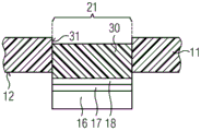
根据图1示出第一电路载体11,第一电路载体带有由印刷电路板材料、例如基于环氧化物的系统、例如FR4制成的第一装配侧12,并示出第二电路载体13,第二电路载体带有由陶瓷、例如Al2O3、Si3N4或AlN制成的第二装配侧14。两个电路载体11、13构成空穴15,两个构件16安装在所述空穴中。构件16通过钎焊连接17分别与第一装配侧12和第二装配侧14相连接。为此,两个装配侧12、14提供用于进行电接触的接触路径18。此外,第一电路载体11通过粘合连接部19与第二电路载体13导电连接,由此将空穴15向外密封。
空穴15通过第一电路载体11中的凹陷20构成。在该凹陷内部埋设了构件16。此外,还为构件16设置了接触区域21,所述接触区域在装配侧12 上承载接触路径18。此外,接触区域21与电路载体11的其他部分相比还通过更大的弹性可挠曲地构造,这根据图1通过印刷电路板的材料的减薄部实现。由此在电路载体11的与该装配侧相对置的一侧上形成凹陷,所述凹陷定义接触区域21。如图1所示,在装配时例如将质量块22安装在接触区域 21,所述质量块为辅助接合而将重力G施加在第一电路载体11上。
如图2所示,第一电路载体11构造了由多个层23组成的层压板,所述层被层压入电路载体的材料24中。其中一个层23构成减薄的接触区域21,接触路径18连同构件16布置在该接触区域上。此外,减薄部还可以设置有遮挡部25,以便向外保护将该区域。
根据图3,接触区域21通过装配侧12中的缝隙26相对于其余的电路载体11分隔开。在缝隙之间构造有连接条27,所述连接条发挥弯曲梁的作用,从而由此形成极具弹性的区域。连接条此外还将装配区域21与其余的电路载体11相连。装配区域21具有未示出的用于装配的构件。缝隙26构造为电路载体11中的贯穿孔,从而当通过两个电路载体11、13构成的空穴应该向外被密封时,能够通过未示出的方式类似于图2地设置遮挡部25。
而且还可以将根据图3的结构安置在根据图1或2减薄的装配区域21 中,以便实现弹性的额外提高。这也适用于根据图4的结构,该结构将在以下予以说明。
在图4中示出,接触区域21在边缘处被凹槽28包镶,所述凹槽交替地设置在电路载体11的第一装配侧12和与该装配侧12相对置的对侧29中。由此形成了一种结构,该结构与波纹管或扩音器膜的边缘结构相类似并且具有极低的抗弯曲性。因此接触区域21易于垂直于接合方向运动。
在图5中,配合件30作为接触区域21安置在留空部31中,其中,接触区域21的挠曲性在该实施例中由此确保,即,配合件30在留空部31中垂直于第一装配侧12的定向是可动的。在此,必须克服在由于配合件的过盈所形成的压配合或过渡配合中因摩擦所致形成的阻力。
最后,在图6中,接触区域21通过由聚硅氧烷膜制成的弹性覆层32构成,所述覆层在凹陷中安置在电路载体11上并且固定在电路载体上(例如通过未示出的粘接)并且构成第一装配侧11。覆层与电路载体11的例如通过印刷电路板材料构成的其余部分相比更具弹性。
在图7中示出用于电子组件的装配过程。图中清晰示出,要么基于有意的制备过程所期望的,要么基于接合配合件的尺寸公差——尤其两个电路载体11、13、构件16和烧结模制件33的尺寸公差,在组件的预装配状态下保留接合缝隙34:根据在哪个电路载体11、13上预装配构件16,与相关的烧结模制件33相对置地形成接合缝隙(然而也可以考虑其他结构方式)。
为了弥合该接合缝隙,可以在烧结过程中向第一电路载体11施加接合力F,从而使弹性的接触区域21根据虚线所示的弯曲线35变形,由此关闭接合缝隙34。同时还通过接合力F形成足以借助烧结模制件33构造烧结连接的压力(显然也必须保持相应的接合温度)。
在图8中示出,当接合力F施加在构件复合件上时,弹性实施的装配侧 12如何在构件16(或能够取代所示钎焊连接所布置的烧结模制件,如图7所示)过盈时变形。在随后的钎焊过程中,通过覆层32的弹性变形将接合力F 至少部分地传递至构造的钎焊连接部,从而能够可靠地构造钎焊连接部。
Claims (13)
1.一种电子组件,其具有
-带有用于电子构件的第一装配侧(12)的第一电路载体(11),
-带有用于电子构件的第二装配侧(14)的第二电路载体(13),其中,第二电路载体(13)利用第二装配侧(14)面向第一电路载体(11)的第一装配侧(12)地与第一电路载体相连接,
-至少一个电子构件(16),所述电子构件不仅与第一装配侧(12)还与第二装配侧(14)相连接,
其特征在于,在第一电路载体(11)与构件(16)之间构造的接触区域(21)中的第一电路载体(11)
-与围绕接触区域(21)的第一电路载体(11)相比并且
-与第二电路载体(13)相比
沿垂直于第一装配侧(12)的方向可挠曲地实施,
其中,接触区域(21)的边缘通过凹空部被削弱,凹空部由凹槽(28)形成,其中,设有多个平行延伸的凹槽(28),其中,所述凹槽交替地引入到第一电路载体(11)的第一装配侧(12)和与第一装配侧(12)背离的对侧(29)中。
2.根据权利要求1所述的组件,其特征在于,接触区域(21)由覆层(32)组成,所述覆层的材料具有与其余的第一电路载体(11)的材料相比更大的弹性。
3.根据权利要求2所述的组件,其特征在于,弹性的覆层(32)由聚硅氧烷制成。
4.根据权利要求1所述的组件,其特征在于,在接触区域(21)中第一电路载体(11)的材料与围绕该接触区域的电路载体相比减薄。
5.根据权利要求4所述的组件,其特征在于,减薄的区域的材料被层压入第一电路载体(11)中并且在接触区域(21)中敞露。
6.根据权利要求5所述的组件,其特征在于,减薄的区域的材料是聚酰亚胺。
7.根据权利要求1所述的组件,其特征在于,第一电路载体(11)在第一装配侧(12)中和/或第二电路载体(13)在第二装配侧(14)中具有凹陷(20),构件(16)处于所述凹陷中。
8.根据权利要求7所述的组件,其特征在于,第一电路载体(11)和第二电路载体(13)构成向外封闭的空穴(15)。
9.根据权利要求1所述的组件,其特征在于,构件(16)与第一装配侧(12)和/或第二装配侧(14)材料接合地相连。
10.根据权利要求9所述的组件,其特征在于,构件(16)与第一装配侧(12)和/或第二装配侧(14)摩擦配合地相连。
11.一种用于接合根据上述权利要求中任一项所述的电子组件的方法,其特征在于,
-将构件(16)装载至第一电路载体(11)或第二电路载体(13),
-随后将第一电路载体(11)与第二电路载体(13)相接合,并且
-构造所述构件与第一电路载体(11)和/或第二电路载体(13)之间的连接。
12.根据权利要求11所述的方法,其特征在于,第一电路载体(11)、第二电路载体(13)和构件(16)之间的至少一部分连接通过烧结和/或通过钎焊和/或通过可导电的传导粘合剂构造。
13.根据权利要求11或12所述的方法,其特征在于,在第一电路载体(11)与第二电路载体(13)连接时将接合力F施加在可挠曲的接触区域(21)上。
Applications Claiming Priority (3)
| Application Number | Priority Date | Filing Date | Title |
|---|---|---|---|
| EP16170185.9 | 2016-05-18 | ||
| EP16170185.9A EP3246941A1 (de) | 2016-05-18 | 2016-05-18 | Elektronische baugruppe mit einem zwischen zwei schaltungsträgern angeordneten bauelement und verfahren zum fügen einer solchen baugruppe |
| PCT/EP2017/060361 WO2017198447A1 (de) | 2016-05-18 | 2017-05-02 | Elektronische baugruppe mit einem zwischen zwei schaltungsträgern angeordneten bauelement und verfahren zum fügen einer solchen baugruppe |
Publications (2)
| Publication Number | Publication Date |
|---|---|
| CN109219875A CN109219875A (zh) | 2019-01-15 |
| CN109219875B true CN109219875B (zh) | 2020-06-19 |
Family
ID=56068705
Family Applications (1)
| Application Number | Title | Priority Date | Filing Date |
|---|---|---|---|
| CN201780030565.6A Active CN109219875B (zh) | 2016-05-18 | 2017-05-02 | 电子组件和用于接合该电子组件的方法 |
Country Status (5)
| Country | Link |
|---|---|
| US (1) | US10420220B2 (zh) |
| EP (2) | EP3246941A1 (zh) |
| JP (1) | JP6823669B2 (zh) |
| CN (1) | CN109219875B (zh) |
| WO (1) | WO2017198447A1 (zh) |
Families Citing this family (2)
| Publication number | Priority date | Publication date | Assignee | Title |
|---|---|---|---|---|
| EP3246941A1 (de) | 2016-05-18 | 2017-11-22 | Siemens Aktiengesellschaft | Elektronische baugruppe mit einem zwischen zwei schaltungsträgern angeordneten bauelement und verfahren zum fügen einer solchen baugruppe |
| DE102017211330A1 (de) * | 2017-07-04 | 2019-01-10 | Siemens Aktiengesellschaft | Toleranzausgleichselement für Schaltbilder |
Citations (4)
| Publication number | Priority date | Publication date | Assignee | Title |
|---|---|---|---|---|
| US8033014B2 (en) * | 2008-07-07 | 2011-10-11 | Unimicron Technology Corp. | Method of making a molded interconnect device |
| DE102014206608A1 (de) * | 2014-04-04 | 2015-10-08 | Siemens Aktiengesellschaft | Verfahren zum Montieren eines elektrischen Bauelements, bei der eine Haube zum Einsatz kommt, und zur Anwendung in diesem Verfahren geeignete Haube |
| CN105529277A (zh) * | 2014-10-20 | 2016-04-27 | 英飞凌科技股份有限公司 | 用于将电路载体与载体板焊接的方法 |
| CN105575936A (zh) * | 2014-10-30 | 2016-05-11 | 英飞凌科技股份有限公司 | 电路载体和制造方法及制造和运行电路装置的方法 |
Family Cites Families (7)
| Publication number | Priority date | Publication date | Assignee | Title |
|---|---|---|---|---|
| US4563725A (en) * | 1983-01-06 | 1986-01-07 | Welwyn Electronics Limited | Electrical assembly |
| US5904499A (en) * | 1994-12-22 | 1999-05-18 | Pace; Benedict G | Package for power semiconductor chips |
| US7906376B2 (en) | 2008-06-30 | 2011-03-15 | Intel Corporation | Magnetic particle-based composite materials for semiconductor packages |
| JP5637156B2 (ja) * | 2012-02-22 | 2014-12-10 | トヨタ自動車株式会社 | 半導体モジュール |
| US9355997B2 (en) * | 2014-03-12 | 2016-05-31 | Invensas Corporation | Integrated circuit assemblies with reinforcement frames, and methods of manufacture |
| DE102014206601A1 (de) | 2014-04-04 | 2015-10-08 | Siemens Aktiengesellschaft | Verfahren zum Montieren eines elektrischen Bauelements, bei der eine Haube zum Einsatz kommt, und zur Anwendung in diesem Verfahren geeignete Haube |
| EP3246941A1 (de) | 2016-05-18 | 2017-11-22 | Siemens Aktiengesellschaft | Elektronische baugruppe mit einem zwischen zwei schaltungsträgern angeordneten bauelement und verfahren zum fügen einer solchen baugruppe |
-
2016
- 2016-05-18 EP EP16170185.9A patent/EP3246941A1/de not_active Withdrawn
-
2017
- 2017-05-02 EP EP17720498.9A patent/EP3443589B1/de active Active
- 2017-05-02 JP JP2018560067A patent/JP6823669B2/ja active Active
- 2017-05-02 WO PCT/EP2017/060361 patent/WO2017198447A1/de unknown
- 2017-05-02 CN CN201780030565.6A patent/CN109219875B/zh active Active
- 2017-05-02 US US16/301,064 patent/US10420220B2/en active Active
Patent Citations (4)
| Publication number | Priority date | Publication date | Assignee | Title |
|---|---|---|---|---|
| US8033014B2 (en) * | 2008-07-07 | 2011-10-11 | Unimicron Technology Corp. | Method of making a molded interconnect device |
| DE102014206608A1 (de) * | 2014-04-04 | 2015-10-08 | Siemens Aktiengesellschaft | Verfahren zum Montieren eines elektrischen Bauelements, bei der eine Haube zum Einsatz kommt, und zur Anwendung in diesem Verfahren geeignete Haube |
| CN105529277A (zh) * | 2014-10-20 | 2016-04-27 | 英飞凌科技股份有限公司 | 用于将电路载体与载体板焊接的方法 |
| CN105575936A (zh) * | 2014-10-30 | 2016-05-11 | 英飞凌科技股份有限公司 | 电路载体和制造方法及制造和运行电路装置的方法 |
Also Published As
| Publication number | Publication date |
|---|---|
| EP3246941A1 (de) | 2017-11-22 |
| JP6823669B2 (ja) | 2021-02-03 |
| CN109219875A (zh) | 2019-01-15 |
| EP3443589B1 (de) | 2021-09-29 |
| US10420220B2 (en) | 2019-09-17 |
| EP3443589A1 (de) | 2019-02-20 |
| JP2019515512A (ja) | 2019-06-06 |
| US20190191566A1 (en) | 2019-06-20 |
| WO2017198447A1 (de) | 2017-11-23 |
Similar Documents
| Publication | Publication Date | Title |
|---|---|---|
| JP6929321B2 (ja) | 電気素子および電気素子の製造方法 | |
| KR100849592B1 (ko) | 파워 모듈 구조 및 이것을 이용한 솔리드 스테이트 릴레이 | |
| CA2616793C (en) | Bending-type rigid printed wiring board and process for producing the same | |
| US10576912B2 (en) | Circuit assembly and electrical junction box | |
| CN108091486B (zh) | 电子部件 | |
| KR20120032514A (ko) | 적어도 2 개의 인쇄회로기판 영역들로 구성되는 인쇄회로기판을 제조하는 방법, 및 인쇄회로기판 | |
| JP2006073763A (ja) | 多層基板の製造方法 | |
| US9480172B2 (en) | Method for producing a printed circuit board consisting of at least two printed circuit board regions, and printed circuit board | |
| US20170339783A1 (en) | SemiFlexible Printed Circuit Board With Embedded Component | |
| CN109219875B (zh) | 电子组件和用于接合该电子组件的方法 | |
| JP2014531009A (ja) | 挿入される回路支持体と囲繞側回路支持体との間に複数のはんだ付けブリッジ若しくは常温接点を備えた変速機制御モジュール | |
| KR20140107270A (ko) | 자동차용 제어 장치 및 자동차용 제어 장치의 제조 방법 | |
| JP4848252B2 (ja) | 端子要素を備えたパワー半導体モジュール | |
| JP5587152B2 (ja) | 電気接続箱 | |
| US8053884B2 (en) | Power semiconductor module with sealing device for sealing to a substrate carrier and method for manufacturing it | |
| KR20190098218A (ko) | 가요성 회로 상의 접촉 표면을 금속 접촉부와 접촉시키는 방법, 크림핑 부품, 가요성 회로와 금속 접촉부의 연결부, 및 제어 장치 | |
| WO2016129278A1 (ja) | フレキシブル基板、フレキシブル基板付き部品、及びフレキシブル基板付き部品の製造方法 | |
| JP6101112B2 (ja) | 表面実装コネクタ | |
| CN107211531A (zh) | 电子部件以及用于生产电子部件的方法 | |
| US20130128480A1 (en) | Circuit arrangement for electronic and/or electrical components | |
| JP4549406B2 (ja) | 電子部品搭載構造及び車載用センサー | |
| JP2017060037A (ja) | 撮像装置 | |
| JP2017050479A (ja) | プリント基板積層体 | |
| CN113892171A (zh) | 电子模块和电子组件 | |
| JP2013026280A (ja) | 素子内蔵配線基板、及びその製造方法 |
Legal Events
| Date | Code | Title | Description |
|---|---|---|---|
| PB01 | Publication | ||
| PB01 | Publication | ||
| SE01 | Entry into force of request for substantive examination | ||
| SE01 | Entry into force of request for substantive examination | ||
| GR01 | Patent grant | ||
| GR01 | Patent grant |