CN108880552B - A kind of SAR-ADC against single event effect - Google Patents
A kind of SAR-ADC against single event effect Download PDFInfo
- Publication number
- CN108880552B CN108880552B CN201810729951.0A CN201810729951A CN108880552B CN 108880552 B CN108880552 B CN 108880552B CN 201810729951 A CN201810729951 A CN 201810729951A CN 108880552 B CN108880552 B CN 108880552B
- Authority
- CN
- China
- Prior art keywords
- comparator
- copy
- dac
- sar
- reinforced
- Prior art date
- Legal status (The legal status is an assumption and is not a legal conclusion. Google has not performed a legal analysis and makes no representation as to the accuracy of the status listed.)
- Active
Links
Images


Classifications
-
- H—ELECTRICITY
- H03—ELECTRONIC CIRCUITRY
- H03M—CODING; DECODING; CODE CONVERSION IN GENERAL
- H03M1/00—Analogue/digital conversion; Digital/analogue conversion
- H03M1/12—Analogue/digital converters
- H03M1/34—Analogue value compared with reference values
- H03M1/38—Analogue value compared with reference values sequentially only, e.g. successive approximation type
Landscapes
- Engineering & Computer Science (AREA)
- Theoretical Computer Science (AREA)
- Analogue/Digital Conversion (AREA)
Abstract
本发明提供一种抗单粒子效应的SAR‑ADC,包括控制逻辑、加固的SAR算法模块、比较器、比较器副本、权电容数模转换器DAC、权电容数模转换器的复制DAC副本、时钟处理模块及数据处理模块。本发明对现有的抗单粒子效应的权电容式SAR‑ADC的设计进行改进,可以在具有更好的可靠性的基础上提高电路的面积及功耗,可应用于航空航天,医疗器械等具有较强辐射环境下的数据转化,通过对易受单粒子影响的电路结构进行冗余提高系统或器件工作的可靠性。
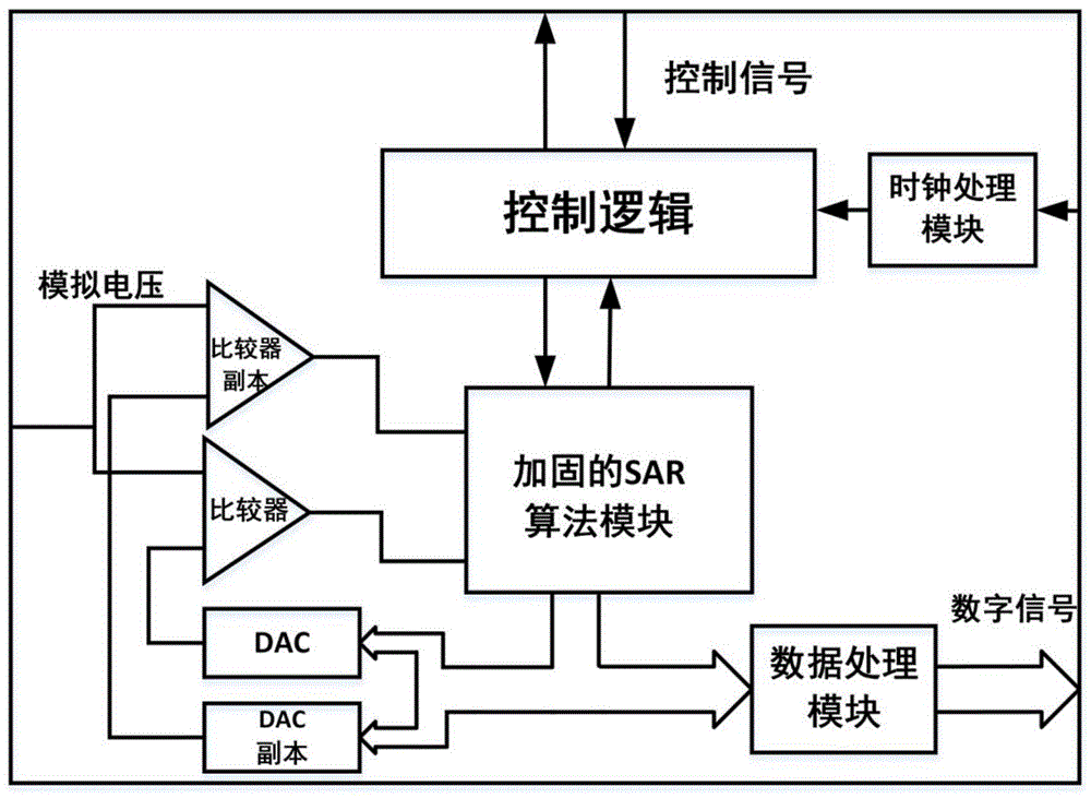
The present invention provides a single event effect-resistant SAR-ADC, comprising control logic, a reinforced SAR algorithm module, a comparator, a copy of the comparator, a DAC of a weight-capacitance digital-to-analog converter, a copy of a DAC copy of the weight-capacitance digital-to-analog converter, Clock processing module and data processing module. The invention improves the design of the existing weighted capacitive SAR-ADC against single event effect, can improve the area and power consumption of the circuit on the basis of better reliability, and can be applied to aerospace, medical equipment, etc. With data conversion in a strong radiation environment, the reliability of the system or device operation is improved by redundancy of the circuit structure that is easily affected by single particles.
Description
技术领域technical field
本发明涉及一种抗单粒子效应的SAR-ADC,属于集成电路技术领域。The invention relates to an anti-single event effect SAR-ADC, which belongs to the technical field of integrated circuits.
背景技术Background technique
ADC是连接模拟系统和数字系统的关键器件,被广泛应用于各种领域。在航天及医疗等具有辐射的工作环境中,存在较多的高能粒子,这些粒子打击到ADC中的一些器件时会产生额外的电子空穴对,从而造成单粒子效应。ADC is a key device that connects analog and digital systems, and is widely used in various fields. In the working environment with radiation such as aerospace and medical treatment, there are many high-energy particles. When these particles hit some devices in the ADC, additional electron-hole pairs will be generated, resulting in the single event effect.
SAR是逐次逼近的简写,SAR-ADC是通过逐次逼近的方法使输出数字信号去逼近输入模拟电压的电压值。由于其高的转换精度和较低的功耗,是大多数应用中的首选器件。其中权电容式的SAR-ADC是SAR-ADC中的一种常用结构。现有一些针对SAR-ADC的单粒子效应加固技术。主要有radiation-hardened by design,这种加固技术主要是在集成电路制造工艺中通过改变布局布线的方式来提高芯片的抗辐射能力;其次是被动固化,这种方法是在电路设计时加入一些无源元件以牺牲性能的方式来提高芯片的抗辐射能力;以及在设计中固化,主要是对电路采取冗余技术以牺牲面积的方式来提高芯片的抗辐射能力。SAR is the abbreviation of successive approximation. SAR-ADC makes the output digital signal approximate the voltage value of the input analog voltage by the method of successive approximation. It is the device of choice in most applications due to its high conversion accuracy and low power consumption. Among them, the weighted capacitive SAR-ADC is a common structure in SAR-ADC. There are some single event effect hardening techniques for SAR-ADC. There are mainly radiation-hardened by design, this kind of reinforcement technology is mainly to improve the radiation resistance of the chip by changing the layout and wiring method in the integrated circuit manufacturing process; followed by passive curing, this method is to add some non-ferrous metals in the circuit design. The source components improve the radiation resistance of the chip by sacrificing performance; and solidified in the design, mainly adopting redundancy technology for the circuit to improve the radiation resistance of the chip by sacrificing the area.
现有的权电容式SAR-ADC的结构如附图1所示,其中权电容式模转换器DAC的原理图如附图5所示,电容C0的值一般很小,大约为10~几十法拉,在辐射环境下极容易受单粒子效应影响使其储存的电荷量发生变化从而使输出的转换结果偏大或者偏小。The structure of the existing weighted capacitive SAR-ADC is shown in Figure 1, and the schematic diagram of the weighted capacitive mode converter DAC is shown in Figure 5. The value of the capacitor C0 is generally small, about 10 to tens of tens of Farah is easily affected by the single event effect in the radiation environment, so that the amount of stored charge changes, so that the output conversion result is larger or smaller.
现有的加固技术主要有在电路上使用两个或多个ADC,即对整个ADC进行冗余,使电路的面积成倍地增长,同时也加大了系统的功耗。The existing reinforcement technology mainly includes using two or more ADCs on the circuit, that is, redundancy of the entire ADC, which doubles the area of the circuit and increases the power consumption of the system at the same time.
发明内容SUMMARY OF THE INVENTION
针对现有技术的不足,本发明提供一种抗单粒子效应的SAR-ADC,在保持与现有技术相当的可靠性的前提下,同时减少权电容式SAR-ADC的面积,通过对最敏感的权电容DAC进行冗余,提高小电容受到辐射影响时的抵抗力从而达到提高芯片可靠性的目的。In view of the deficiencies of the prior art, the present invention provides a single event effect-resistant SAR-ADC, which reduces the area of the capacitive SAR-ADC while maintaining the same reliability as the prior art. The weight of the capacitor DAC is redundant to improve the resistance of small capacitors when they are affected by radiation, so as to achieve the purpose of improving chip reliability.
为达到上述目的,本发明的技术方案是这样实现的:In order to achieve the above object, the technical scheme of the present invention is achieved in this way:
一种抗单粒子效应的SAR-ADC,包括控制逻辑、加固的SAR算法模块、比较器、比较器副本、权电容数模转换器DAC、权电容数模转换器的复制DAC副本、时钟处理模块及数据处理模块,An anti-single event effect SAR-ADC, comprising control logic, a reinforced SAR algorithm module, a comparator, a copy of the comparator, a weight-capacitance digital-to-analog converter DAC, a copy of the weight-capacitance digital-to-analog converter DAC, and a clock processing module and data processing module,
所述控制逻辑接收用户输入的控制信号并根据输入的控制信号调整工作状态,同时接收加固的SAR算法模块的反馈信号用于判断目前的状态,所述控制逻辑向用户输出中断信号,便于用户控制,同时输出控制信号至加固的SAR算法模块;The control logic receives the control signal input by the user and adjusts the working state according to the input control signal, and at the same time receives the feedback signal of the reinforced SAR algorithm module for judging the current state, the control logic outputs the interrupt signal to the user, which is convenient for the user to control , and output the control signal to the reinforced SAR algorithm module at the same time;
所述加固的SAR算法模块接收控制逻辑的控制信号,并输出反馈信号给控制逻辑;同时加固的SAR算法模块接收控制信号后根据比较器和比较器副本的输入将转换后的数字数据传输出至权电容数模转换器DAC和权电容数模转换器的复制DAC副本以及数据处理模块;The reinforced SAR algorithm module receives the control signal of the control logic, and outputs a feedback signal to the control logic; at the same time, the reinforced SAR algorithm module receives the control signal and transmits the converted digital data according to the input of the comparator and the copy of the comparator. Weight-capacitance digital-to-analog converter DAC and weight-capacitance digital-to-analog converter replica DAC copy and data processing module;
所述电容数模转换器DAC及DAC副本接收加固的SAR算法模块输出的数字数据后转化为模拟电压并分别传输出至所述比较器和比较器副本;The capacitance digital-to-analog converter DAC and the DAC copy receive the digital data output by the reinforced SAR algorithm module and convert it into an analog voltage and transmit it to the comparator and the comparator copy respectively;
所述比较器和比较器副本的一个输入分别接收权电容数模转换器DAC及DAC副本的转换结果,另一个输入同时输入相同的模拟电压,并将比较后的结果传输出至加固的SAR算法模块;One input of the comparator and the copy of the comparator receives the conversion results of the weighted capacitance digital-to-analog converter DAC and the copy of the DAC respectively, and the other input simultaneously inputs the same analog voltage, and transmits the compared result to the hardened SAR algorithm module;
所述数据处理模块接收加固的SAR算法模块输出的数字数据,并通过通信协议为用户输出不同协议类型的数字信号;The data processing module receives the digital data output by the reinforced SAR algorithm module, and outputs digital signals of different protocol types for the user through the communication protocol;
所述时钟处理模块接收外部输入时钟并将其进行倍频处理后输出至控制逻辑。The clock processing module receives the external input clock, performs frequency multiplication processing and outputs it to the control logic.
优选地,所述加固的SAR算法模块接收比较器和比较器副本的输出并对其进行比较,实现对DAC和DAC副本是否受单粒子效应影响的判断。Preferably, the hardened SAR algorithm module receives and compares the outputs of the comparators and the replicas of the comparators, so as to determine whether the DACs and the replicas of the DACs are affected by single event effects.
优选地,所述电容数模转换器DAC采用双模冗余处理,所述比较器根据电容数模转换器DAC的冗余进行相应的双模冗余处理。Preferably, the capacitance digital-to-analog converter DAC adopts dual-mode redundancy processing, and the comparator performs corresponding dual-mode redundancy processing according to the redundancy of the capacitance digital-to-analog converter DAC.
有益效果:本发明提供一种抗单粒子效应的SAR-ADC,对现有的抗单粒子效应的权电容式SAR-ADC的设计进行改进,可以在具有更好的可靠性的基础上提高电路的面积及功耗,可应用于航空航天,医疗器械等具有较强辐射环境下的数据转化,通过对易受单粒子影响的电路结构进行冗余提高系统或器件工作的可靠性。Beneficial effects: The present invention provides a single-event effect-resistant SAR-ADC, improves the design of the existing single-event effect-resistant weighted capacitive SAR-ADC, and can improve the circuit on the basis of better reliability. The area and power consumption can be applied to data conversion in aerospace, medical equipment and other environments with strong radiation, and the reliability of system or device operation can be improved by redundancy of circuit structures that are easily affected by single particles.
附图说明Description of drawings
图1是现有SAR-ADC的标准结构;Figure 1 is the standard structure of the existing SAR-ADC;
图2是本发明的加固SAR-ADC的总体框架图;Fig. 2 is the overall frame diagram of the reinforcement SAR-ADC of the present invention;
图3是本发明的加固结构的框架。;Figure 3 is a frame of the reinforcement structure of the present invention. ;
图4是权电容式DAC的一般结构。Figure 4 shows the general structure of a capacitive DAC.
图5是本发明所设计的加固的SAR算法模块中对比较器和比较器副本的输入信号的判同方法;Fig. 5 is the identification method to the input signal of comparator and comparator replica in the reinforced SAR algorithm module designed by the present invention;
图6是用于控制数模转换器DAC中电容充放电的开关原理图。FIG. 6 is a schematic diagram of a switch used to control charging and discharging of a capacitor in a digital-to-analog converter DAC.
具体实施方式Detailed ways
为了使本技术领域的人员更好地理解本申请中的技术方案,下面对本申请实施例中的技术方案进行清楚、完整地描述,显然,所描述的实施例仅仅是本申请一部分实施例,而不是全部的实施例。基于本申请中的实施例,本领域普通技术人员在没有做出创造性劳动前提下所获得的所有其他实施例,都应当属于本申请保护的范围。In order to make those skilled in the art better understand the technical solutions in the present application, the technical solutions in the embodiments of the present application will be described clearly and completely below. Obviously, the described embodiments are only a part of the embodiments of the present application, and Not all examples. Based on the embodiments in the present application, all other embodiments obtained by those of ordinary skill in the art without creative work shall fall within the scope of protection of the present application.
一种抗单粒子效应的SAR-ADC,包括控制逻辑、加固的SAR算法模块、比较器、比较器副本、权电容数模转换器DAC、权电容数模转换器的复制DAC副本、时钟处理模块及数据处理模块,An anti-single event effect SAR-ADC, comprising control logic, a reinforced SAR algorithm module, a comparator, a copy of the comparator, a weight-capacitance digital-to-analog converter DAC, a copy of the weight-capacitance digital-to-analog converter DAC, and a clock processing module and data processing module,
所述控制逻辑接收用户输入的控制信号并根据输入的控制信号调整工作状态,同时接收加固的SAR算法模块的反馈信号用于判断目前的状态,所述控制逻辑向用户输出中断信号,便于用户控制,同时输出控制信号至加固的SAR算法模块;The control logic receives the control signal input by the user and adjusts the working state according to the input control signal, and simultaneously receives the feedback signal of the reinforced SAR algorithm module for judging the current state. The control logic outputs an interrupt signal to the user, which is convenient for the user to control , and output the control signal to the reinforced SAR algorithm module at the same time;
所述加固的SAR算法模块接收控制逻辑的控制信号,并输出反馈信号给控制逻辑;同时加固的SAR算法模块接收控制信号后根据比较器的输入将转换后的数字数据传输出至权电容数模转换器DAC和权电容数模转换器的复制DAC副本以及数据处理模块;The reinforced SAR algorithm module receives the control signal of the control logic, and outputs a feedback signal to the control logic; at the same time, the reinforced SAR algorithm module transmits the converted digital data to the weighted capacitance digital-analog according to the input of the comparator after receiving the control signal. Replica DAC copy of converter DAC and weight capacitance digital-to-analog converter and data processing module;
所述电容数模转换器DAC及DAC副本接收加固的SAR算法模块输出的数字数据后转化为模拟电压并分别传输出至所述比较器和比较器副本;The capacitance digital-to-analog converter DAC and the DAC copy receive the digital data output by the reinforced SAR algorithm module and convert it into an analog voltage and transmit it to the comparator and the comparator copy respectively;
所述比较器和比较器副本的一个输入分别接收权电容数模转换器DAC及DAC副本的转换结果,另一个输入同时输入相同的模拟电压,并将比较后的结果传输出至加固的SAR算法模块;One input of the comparator and the copy of the comparator receives the conversion results of the weighted capacitance digital-to-analog converter DAC and the copy of the DAC respectively, and the other input simultaneously inputs the same analog voltage, and transmits the compared result to the hardened SAR algorithm module;
所述数据处理模块接收加固的SAR算法模块输出的数字数据,并通过通信协议为用户输出不同协议类型的数字信号;The data processing module receives the digital data output by the reinforced SAR algorithm module, and outputs digital signals of different protocol types for the user through the communication protocol;
所述时钟处理模块接收外部输入时钟并将其进行倍频处理后输出至控制逻辑。The clock processing module receives the external input clock, performs frequency multiplication processing and outputs it to the control logic.
优选地,所述加固的SAR算法模块将比较器和比较器副本的输出进行比较,实现对DAC和DAC副本是否受单粒子效应影响的判断,其比较原理如图5所示,其中a为比较器的输出结果,b为比较器副本的输出结果,当a=b时算法继续运行,当a!=b时等待输入a=b,同时对所述加固的SAR算法模块中的关键触发器采用三模冗余技术进行处理。Preferably, the reinforced SAR algorithm module compares the outputs of the comparator and the replica of the comparator to determine whether the DAC and the replica of the DAC are affected by the single event effect. The comparison principle is shown in Figure 5, where a is the comparison The output result of the comparator, b is the output result of the copy of the comparator, when a=b, the algorithm continues to run, when a! When =b, wait for a=b to be input, and at the same time, use three-mode redundancy technology to process the key triggers in the reinforced SAR algorithm module.
优选地,所述电容数模转换器DAC采用双模冗余处理,所述比较器根据电容数模转换器DAC的冗余进行相应的双模冗余处理。本发明中,所述DAC副本为模转换器DAC的复制,综合考虑面积和可靠性,对DAC进行双模冗余提高其容错性能,在面积允许的情况下可采取也可采用三模冗余,此时,比较器根据电容数模转换器DAC的冗余进行相应的三模冗余处理。Preferably, the capacitance digital-to-analog converter DAC adopts dual-mode redundancy processing, and the comparator performs corresponding dual-mode redundancy processing according to the redundancy of the capacitance digital-to-analog converter DAC. In the present invention, the DAC copy is the copy of the analog converter DAC. Considering the area and reliability comprehensively, dual-mode redundancy is performed on the DAC to improve its fault-tolerant performance, and triple-mode redundancy can be adopted when the area allows. , at this time, the comparator performs corresponding three-mode redundancy processing according to the redundancy of the capacitance digital-to-analog converter DAC.
优选地,所述电容数模转换器DAC采用双模冗余处理,所述比较器根据电容数模转换器DAC的冗余进行相应的双模冗余处理。Preferably, the capacitance digital-to-analog converter DAC adopts dual-mode redundancy processing, and the comparator performs corresponding dual-mode redundancy processing according to the redundancy of the capacitance digital-to-analog converter DAC.
本发明中,对权电容数模转换器DAC进行了冗余处理,冗余后形成权电容数模转换器DAC和权电容数模转换器的复制DAC副本,两个DAC的输入一致,当仅其中一个DAC受到单粒子效应影响时两个DAC输出不一致。由于对权电容数模转换器DAC进行了冗余处理,所以需要对比较器进行相同的冗余处理以配合权电容数模转换器DAC的冗余。而在本发明中,由于对比较器进行了冗余处理,在SAR算法模块的算法与比较器的中间需要对输入进行判同,其结构如图5所示,同时对SAR算法模块中的部分D触发器进行了三模冗余处理。In the present invention, redundant processing is performed on the weight-capacitance digital-to-analog converter DAC. The outputs of the two DACs are inconsistent when one of the DACs is affected by the single event effect. Since redundant processing is performed on the weighted capacitance digital-to-analog converter DAC, the comparator needs to be subjected to the same redundant processing to match the redundancy of the weighted capacitance digital-to-analog converter DAC. In the present invention, due to redundant processing of the comparator, the input needs to be identified between the algorithm of the SAR algorithm module and the comparator. Its structure is shown in Figure 5. The D flip-flop is processed with three-mode redundancy.
本发明中提及的控制逻辑、加固的SAR算法模块、时钟处理模块和数据处理模块为数字电路,在本发明中通过Verilog实现其功能后导入Cadence IC,属于常规技术手段。本发明提及的比较器和比较器副本、权电容数模转换器DAC和权电容数模转换器的复制DAC副本为模拟电路。其中,权电容数模转换器DAC和权电容数模转换器的复制DAC副本在CadenceIC中通过原理图绘制来实现,比较器和比较器副本通过verilog-a实现。The control logic, the reinforced SAR algorithm module, the clock processing module and the data processing module mentioned in the present invention are digital circuits. In the present invention, the functions are implemented by Verilog and then imported into the Cadence IC, which are conventional technical means. The comparator and the replica of the comparator, the weight-capacitance digital-to-analog converter DAC and the replica of the weight-capacitance digital-to-analog converter mentioned in the present invention are analog circuits. Among them, the weight-capacitance digital-to-analog converter DAC and the copy DAC copy of the weight-capacitance digital-to-analog converter are implemented in CadenceIC by drawing the schematic diagram, and the comparator and the comparator copy are implemented by verilog-a.
本发明中,控制逻辑根据现有标准ADC的操作时序,使用Verilog语言设计出与其相似的操作逻辑,综合后导入Cadence IC中生成相应的symbol;时钟处理模块采用普遍的计数倍频技术进行倍频;数据处理模块采用标准协议规定的时序图进行设计,其中包含SPI,IIC以及12位串行总线和12位数据并行输出。上述均为常规技术手段,故而未加详述。In the present invention, the control logic uses the Verilog language to design a similar operation logic according to the operation sequence of the existing standard ADC, and imports it into the Cadence IC to generate the corresponding symbol after synthesis; the clock processing module adopts the common counting frequency multiplication technology for frequency multiplication ; The data processing module is designed with the timing diagram specified by the standard protocol, including SPI, IIC, 12-bit serial bus and 12-bit data parallel output. The above are all conventional technical means, so they are not described in detail.
本发明中,加固的SAR算法模块先使用Verilog语言在Verilog编译软件中进行编译仿真,再导出其RTL视图,随后在Cadence IC中根据导出的RTL视图使用D触发器等基本单元参照进行连接,其中对部分D触发器进行三模冗余。具体实现方式如下:In the present invention, the reinforced SAR algorithm module first uses Verilog language to compile and simulate in Verilog compilation software, and then exports its RTL view, and then uses D flip-flops and other basic unit references to connect in Cadence IC according to the exported RTL view, wherein Tri-modular redundancy for some D flip-flops. The specific implementation is as follows:
1)上述的加固的SAR算法模块,其设计的目的为实现输入数据的逐次比较,在比较开始前先给加固的SAR算法模块内的触发器装初值12’b1000_0000_0000,此时针对最高位进行比较,时钟沿到来时将寄存器的值输出给权电容数模转换器DAC及权电容数模转换器的复制DAC副本,DAC和DAC副本将输入的数字信号转换为模拟电压后分别输出给比较器和比较器副本,比较器和比较器副本将输入模拟电压分别与DAC和DAC副本输出的模拟电压进行比较,并将比较后的结果输出给加固的SAR算法模块,加固的SAR算法模块通过附图5的结构对他们进行比较,实现对DAC和DAC副本是否受单粒子效应影响的判断。若s=1,当c=0,则将该位置0,同时将下一位置1,寄存器的值变为12’b0100_0000_0000;当c=1,则将该位置1,同时将下一位置1,寄存器的值变为12’b1100_0000_0000。这样就完成了一位的数据比较,之后进行下一位数据的比较,一直比较到最低位即完成一次转换。根据这一过程通过Verilog语言在Quartus中将其实现并仿真,确认无误后导出RTL视图;1) The purpose of the above-mentioned reinforced SAR algorithm module is to realize the successive comparison of input data. Before the comparison starts, the trigger in the reinforced SAR algorithm module is equipped with an initial value of 12'b1000_0000_0000. For comparison, when the clock edge arrives, the value of the register is output to the weighted capacitance digital-to-analog converter DAC and the duplicate DAC copy of the weighted capacitance digital-to-analog converter. The DAC and the DAC copy convert the input digital signal into an analog voltage and output it to the comparator respectively. And the comparator copy, the comparator and the comparator copy compare the input analog voltage with the analog voltage output by the DAC and the DAC copy respectively, and output the compared result to the reinforced SAR algorithm module. The reinforced SAR algorithm module passes the attached picture. The structure of 5 compares them to realize the judgment of whether the DAC and the DAC copy are affected by the single event effect. If s=1, when c=0, set this position to 0, and set the next position to 1 at the same time, the value of the register becomes 12'b0100_0000_0000; when c=1, set this position to 1, and set the next position to 1 at the same time, The value of the register becomes 12'b1100_0000_0000. In this way, the data comparison of one bit is completed, and then the comparison of the next bit of data is performed, and a conversion is completed until the lowest bit is compared. According to this process, it is implemented and simulated in Quartus through Verilog language, and the RTL view is exported after confirming that it is correct;
2)导出RTL视图后在Cadence IC中利用门和D触发器等基本原件参照RTL视图进行连接,并对部分D触发器进行三模冗余处理,在本次设计发明中由于高位D触发器的权重较大,我们对高6位D触发器进行了三模冗余。2) After exporting the RTL view, use the basic elements such as gates and D flip-flops in Cadence IC to connect with reference to the RTL view, and perform three-mode redundancy processing on some D flip-flops. In this design invention, due to the high-order D flip-flops With larger weights, we have triple-modular redundancy for the upper 6-bit D flip-flops.
本发明中,权电容数模转换器DAC的设计原理如图4所示,通过加固的SAR算法模块输出的12位数据b0~b11对12个电容进行充放电的控制,当bn=0时电容Cn一端接地实现放电,当bn=1当bn=0时电容Cn一端接参考电压Vref实现充电。输出电压与电容的电荷量相关其输出电压Vout为:In the present invention, the design principle of the weight-capacitance digital-to-analog converter DAC is shown in Figure 4. The 12-bit data b0-b11 output by the reinforced SAR algorithm module is used to control the charge and discharge of 12 capacitors. When bn=0, the capacitors are charged and discharged. One end of Cn is grounded to realize discharge, and when bn=1 and bn=0, one end of capacitor Cn is connected to the reference voltage Vref to realize charging. The output voltage is related to the charge of the capacitor, and the output voltage Vout is:

本发明中,权电容数模转换器DAC和DAC副本的结构完全一致,它们所采用的开关设计的原理图如图6所示。当输入in为1时,NM1和PM1导通,NM2和PM2截至,输出out=ver(参考电压);输入in为0时,NM1和PM1截至,NM2和PM2导通,输出out=gnd。因此实现了通过bn控制电容一端接地还是接参考电压的功能,从而达到数字到模拟的转换效果。In the present invention, the structures of the weight-capacitance digital-to-analog converter DAC and the DAC copy are completely the same, and the schematic diagram of the switch design used by them is shown in FIG. 6 . When input in is 1, NM1 and PM1 are turned on, NM2 and PM2 are turned off, and output out=ver (reference voltage); when input in is 0, NM1 and PM1 are turned off, NM2 and PM2 are turned on, and output out=gnd. Therefore, the function of controlling whether one end of the capacitor is grounded or connected to the reference voltage through bn is realized, so as to achieve the conversion effect from digital to analog.
本发明中,完成了权电容数模转换器DAC和DAC副本的设计后将其进行备份,并对其进行双模冗余处理,如附图3所示,将其输入同时与加固的SAR算法模块的输出相连使它们具有相同的输入,并将他们的输出分别与比较器和比较器副本的一个输入连接。In the present invention, after the design of the DAC and the DAC copy of the weight-capacitance digital-to-analog converter is completed, they are backed up, and dual-mode redundancy processing is performed on them. As shown in FIG. 3, they are input into the reinforced SAR algorithm simultaneously The outputs of the blocks are connected so that they have the same input, and their outputs are connected to one input of the comparator and one of the comparator replicas respectively.
为了与冗余后的权电容数模转换器DAC和DAC副本进行连接,对比较器也进行双模冗余得到比较器和比较器副本。In order to connect with the redundant weight-capacitance digital-to-analog converter DAC and the DAC copy, dual-mode redundancy is also performed on the comparator to obtain the comparator and the comparator copy.
为了使上述比较器的精度等参数方便调试,通过verilog-a实现,并对其中设置了如下参数便于调节:包括高阈值电压hys;比较器输入级增益slop;比较器正偏移电压p_off;比较器负偏移电压p_off;比较器输出高电平one;比较器输出低电平zero。In order to facilitate the debugging of the above-mentioned parameters such as the accuracy of the comparator, it is realized by verilog-a, and the following parameters are set for easy adjustment: including high threshold voltage hys; comparator input stage gain slop; comparator positive offset voltage p_off; comparison The negative offset voltage of the comparator is p_off; the comparator outputs a high level one; the comparator outputs a low level zero.
上述比较器根据比较器的原理遵循verilog-a的语法建模后的输出out为:The above comparator follows the syntax of verilog-a according to the principle of the comparator, and the output out is:
out={(one-zero)/2.0}*tanh(slope*(vin-hys/2.0))+(one+zero)/2.0。out={(one-zero)/2.0}*tanh(slope*(vin-hys/2.0))+(one+zero)/2.0.
本发明的一种抗单粒子效应的SAR-ADC,其整体结构如图2所示,针对权电容式SAR-ADC中权电容数模转换器DAC中小电容易受单粒子效应影响这一特性,对其进行双模冗余,当其中一个DAC受到单粒子效应影响时两个DAC的输出将不同,由于两个比较器和比较器副本具有相同输入的模拟电压,所以两个比较器的输出不同,此时通过附图1的判定后输出s=0,c=0。此时SAR算法停止执行,并等待s=1为止;实现了降低冗余面积的情况下,保证了ADC的可靠性。冗余结构下不会产生错误输出,从而以牺牲较小的面积为代价提高了芯片的可靠性。The overall structure of an anti-single event effect SAR-ADC of the present invention is shown in FIG. 2. In view of the characteristic that the small power in the weighted capacitance digital-to-analog converter DAC of the weighted capacitance type SAR-ADC is easily affected by the single event effect, Make it dual mode redundant, the output of the two DACs will be different when one of the DACs is affected by the single event effect, the output of the two comparators will be different because the two comparators and the comparator replicas have the same input analog voltage , at this time, s=0, c=0 is output after the judgment of FIG. 1 . At this time, the SAR algorithm stops executing and waits until s=1; the reliability of the ADC is guaranteed under the condition of reducing the redundant area. No erroneous output will be generated under the redundant structure, thereby improving the reliability of the chip at the expense of a smaller area.
对所公开的实施例的上述说明,使本领域专业技术人员能够实现或使用本发明。对这些实施例的两种修改对本领域的专业技术人员来说将是显而易见的,本文中所定义的一般原理可以在不脱离本发明的精神或范围的情况下,在其它实施例中实现。因此,本发明将不会被限制于本文所示的这些实施例,而是要符合与本文所公开的原理和新颖特点相一致的最宽的范围。The above description of the disclosed embodiments enables any person skilled in the art to make or use the present invention. Both modifications to these embodiments will be readily apparent to those skilled in the art, and the generic principles defined herein may be implemented in other embodiments without departing from the spirit or scope of the invention. Thus, the present invention is not intended to be limited to the embodiments shown herein, but is to be accorded the widest scope consistent with the principles and novel features disclosed herein.
Claims (2)
Priority Applications (1)
| Application Number | Priority Date | Filing Date | Title |
|---|---|---|---|
| CN201810729951.0A CN108880552B (en) | 2018-07-05 | 2018-07-05 | A kind of SAR-ADC against single event effect |
Applications Claiming Priority (1)
| Application Number | Priority Date | Filing Date | Title |
|---|---|---|---|
| CN201810729951.0A CN108880552B (en) | 2018-07-05 | 2018-07-05 | A kind of SAR-ADC against single event effect |
Publications (2)
| Publication Number | Publication Date |
|---|---|
| CN108880552A CN108880552A (en) | 2018-11-23 |
| CN108880552B true CN108880552B (en) | 2022-04-22 |
Family
ID=64299074
Family Applications (1)
| Application Number | Title | Priority Date | Filing Date |
|---|---|---|---|
| CN201810729951.0A Active CN108880552B (en) | 2018-07-05 | 2018-07-05 | A kind of SAR-ADC against single event effect |
Country Status (1)
| Country | Link |
|---|---|
| CN (1) | CN108880552B (en) |
Families Citing this family (1)
| Publication number | Priority date | Publication date | Assignee | Title |
|---|---|---|---|---|
| CN120528401B (en) * | 2025-07-23 | 2025-11-21 | 中国人民解放军国防科技大学 | A radiation-hardened numerically controlled oscillator, clock data recovery circuit and device |
Citations (10)
| Publication number | Priority date | Publication date | Assignee | Title |
|---|---|---|---|---|
| CN102117797A (en) * | 2009-12-30 | 2011-07-06 | 中国科学院微电子研究所 | A CMOS integrated circuit anti-single event radiation hardening circuit |
| CN102820879A (en) * | 2012-08-17 | 2012-12-12 | 中国电子科技集团公司第五十八研究所 | Radiation-proof triple-modular redundancy circuit structure |
| CN103001636A (en) * | 2012-12-11 | 2013-03-27 | 北京时代民芯科技有限公司 | A Single Event Effect Detection Method for Folded Interpolation Analog-to-Digital Converter |
| CN103955448A (en) * | 2014-05-21 | 2014-07-30 | 西安空间无线电技术研究所 | FFT (fast Fourier transform) reinforcing design method with single event upset-resistant capability |
| CN105897267A (en) * | 2016-04-18 | 2016-08-24 | 西北核技术研究所 | Analog-digital converter single particle effect test method and system thereof |
| CN106026999A (en) * | 2016-05-13 | 2016-10-12 | 河海大学常州校区 | CMOS (Complementary Metal Oxide Semiconductors) comparator capable of resisting single event effect |
| CN106877866A (en) * | 2014-12-17 | 2017-06-20 | 美国亚德诺半导体公司 | For the microprocessor assisted calibration of analog-digital converter |
| CN107682012A (en) * | 2017-09-11 | 2018-02-09 | 电子科技大学 | A kind of low complex degree DEM technologies suitable for successive approximation analog-digital converter |
| CN107968656A (en) * | 2016-10-20 | 2018-04-27 | 国民技术股份有限公司 | A kind of successive approximation simulates digital quantizer and its using switching method |
| CN108242929A (en) * | 2017-07-07 | 2018-07-03 | 西安微电子技术研究所 | A kind of more precision Flouride-resistani acid phesphatase logic control devices for SAR types ADC |
Family Cites Families (1)
| Publication number | Priority date | Publication date | Assignee | Title |
|---|---|---|---|---|
| WO2008118353A1 (en) * | 2007-03-23 | 2008-10-02 | Beckman Coulter, Inc. | Multi-gain adaptive linear processing and gated digital system for use in flow cytometry |
-
2018
- 2018-07-05 CN CN201810729951.0A patent/CN108880552B/en active Active
Patent Citations (10)
| Publication number | Priority date | Publication date | Assignee | Title |
|---|---|---|---|---|
| CN102117797A (en) * | 2009-12-30 | 2011-07-06 | 中国科学院微电子研究所 | A CMOS integrated circuit anti-single event radiation hardening circuit |
| CN102820879A (en) * | 2012-08-17 | 2012-12-12 | 中国电子科技集团公司第五十八研究所 | Radiation-proof triple-modular redundancy circuit structure |
| CN103001636A (en) * | 2012-12-11 | 2013-03-27 | 北京时代民芯科技有限公司 | A Single Event Effect Detection Method for Folded Interpolation Analog-to-Digital Converter |
| CN103955448A (en) * | 2014-05-21 | 2014-07-30 | 西安空间无线电技术研究所 | FFT (fast Fourier transform) reinforcing design method with single event upset-resistant capability |
| CN106877866A (en) * | 2014-12-17 | 2017-06-20 | 美国亚德诺半导体公司 | For the microprocessor assisted calibration of analog-digital converter |
| CN105897267A (en) * | 2016-04-18 | 2016-08-24 | 西北核技术研究所 | Analog-digital converter single particle effect test method and system thereof |
| CN106026999A (en) * | 2016-05-13 | 2016-10-12 | 河海大学常州校区 | CMOS (Complementary Metal Oxide Semiconductors) comparator capable of resisting single event effect |
| CN107968656A (en) * | 2016-10-20 | 2018-04-27 | 国民技术股份有限公司 | A kind of successive approximation simulates digital quantizer and its using switching method |
| CN108242929A (en) * | 2017-07-07 | 2018-07-03 | 西安微电子技术研究所 | A kind of more precision Flouride-resistani acid phesphatase logic control devices for SAR types ADC |
| CN107682012A (en) * | 2017-09-11 | 2018-02-09 | 电子科技大学 | A kind of low complex degree DEM technologies suitable for successive approximation analog-digital converter |
Non-Patent Citations (4)
| Title |
|---|
| Single event effects in analog-to-digital converters: device performance and system impact;T.L. Turflinger 等;《IEEE Transactions on Nuclear Science》;19941231;第41卷(第6期);2187-2194 * |
| Total Ionizing Dose Effects of 55-nm Silicon-Oxide-Nitride-Oxide-Silicon Charge Trapping Memory in Pulse and DC Modes;李梅 等;《Chinese Physics Letters》;20180703;第35卷(第7期);135-138 * |
| 基于两步式结构的12bit高速低功耗逐次逼近型ADC研究;蒋佳君;《中国优秀硕士学位论文全文数据库 信息科技辑》;20170215(第02(2017年)期);I135-1125 * |
| 基于标准工艺的模数转换器抗辐照加固设计与验证;陈良;《中国优秀硕士学位论文全文数据库 信息科技辑》;20170215(第02(2017年)期);I135-1109 * |
Also Published As
| Publication number | Publication date |
|---|---|
| CN108880552A (en) | 2018-11-23 |
Similar Documents
| Publication | Publication Date | Title |
|---|---|---|
| US8471751B2 (en) | Two-stage analog-to-digital converter using SAR and TDC | |
| CN109687872B (en) | High-speed digital logic circuit and sampling adjustment method for SAR_ADC | |
| TWI532328B (en) | Analog to digital converter and converting method thereof | |
| CN111934688A (en) | Successive approximation type analog-to-digital converter and method | |
| CN113938135B (en) | Successive approximation analog-to-digital converter and calibration method | |
| CN105897272B (en) | Successive approximation analog-digital converter and its control method | |
| CN110474623B (en) | An offset self-correcting dynamic comparator for successive approximation analog-to-digital converters | |
| CN106209102A (en) | Mixed type two-layer configuration for full parellel successive approximation analog-digital converter | |
| CN104967451A (en) | Successive Approximation Analog-to-Digital Converter | |
| CN102045067A (en) | Conversion and calibration algorithm for improving output signal-to-noise ratio of successive approximation (SAR) analog-to-digital converter (ADC) and ADC | |
| US11133813B2 (en) | Analog to digital converter device and noise shaping digital slope analog to digital converter circuitry | |
| CN105049051B (en) | A kind of successive approximation modulus conversion circuit and the electronic equipment for having the circuit | |
| CN107863966A (en) | A kind of gradually-appoximant analog-digital converter electric capacity optimization method for intelligence sensor | |
| CN117647686A (en) | A high-speed and high-voltage pulse signal acquisition system | |
| CN107231153A (en) | Gradually-appoximant analog-digital converter for monolithic integrated sensor | |
| CN108880552B (en) | A kind of SAR-ADC against single event effect | |
| CN111277270B (en) | High-speed successive approximation type analog-to-digital conversion circuit and DAC weight distribution method | |
| CN106899300A (en) | A kind of redundant cyclic averaging method for gradually-appoximant analog-digital converter | |
| Megha et al. | Design and VLSI implementation of SAR Analog to Digital Converter Using Analog Mixed Signal | |
| CN106685420B (en) | A kind of low-power consumption high linearity switching method of successive approximation analog to digital C capacitor arrays | |
| CN106656192A (en) | ADC chip circuit based on gate voltage bootstrap circuit and segmented full capacitor array | |
| Hu et al. | Energy-efficient, area-efficient, high-accuracy and low-complexity switching scheme for SAR ADC | |
| CN110389746A (en) | Hardware-accelerated circuit, microcontroller chip and system | |
| CN102169140B (en) | Clock frequency detection circuit | |
| CN112583406A (en) | Analog-to-digital converter device and analog-to-digital converter circuit system |
Legal Events
| Date | Code | Title | Description |
|---|---|---|---|
| PB01 | Publication | ||
| PB01 | Publication | ||
| SE01 | Entry into force of request for substantive examination | ||
| SE01 | Entry into force of request for substantive examination | ||
| GR01 | Patent grant | ||
| GR01 | Patent grant |