CN108695067B - Multilayer capacitor and method for manufacturing multilayer capacitor - Google Patents
Multilayer capacitor and method for manufacturing multilayer capacitor Download PDFInfo
- Publication number
- CN108695067B CN108695067B CN201710821519.XA CN201710821519A CN108695067B CN 108695067 B CN108695067 B CN 108695067B CN 201710821519 A CN201710821519 A CN 201710821519A CN 108695067 B CN108695067 B CN 108695067B
- Authority
- CN
- China
- Prior art keywords
- multilayer capacitor
- layer
- electrode
- intermetallic compound
- metal particles
- Prior art date
- Legal status (The legal status is an assumption and is not a legal conclusion. Google has not performed a legal analysis and makes no representation as to the accuracy of the status listed.)
- Active
Links
- 239000003990 capacitor Substances 0.000 title claims abstract description 89
- 238000004519 manufacturing process Methods 0.000 title claims abstract description 15
- 238000000034 method Methods 0.000 title claims description 18
- 229920005989 resin Polymers 0.000 claims abstract description 139
- 239000011347 resin Substances 0.000 claims abstract description 139
- 239000002923 metal particle Substances 0.000 claims abstract description 93
- 229910000765 intermetallic Inorganic materials 0.000 claims abstract description 70
- PXHVJJICTQNCMI-UHFFFAOYSA-N Nickel Chemical compound [Ni] PXHVJJICTQNCMI-UHFFFAOYSA-N 0.000 claims description 77
- 239000010949 copper Substances 0.000 claims description 71
- RYGMFSIKBFXOCR-UHFFFAOYSA-N Copper Chemical group [Cu] RYGMFSIKBFXOCR-UHFFFAOYSA-N 0.000 claims description 61
- 229910052802 copper Inorganic materials 0.000 claims description 61
- 238000002844 melting Methods 0.000 claims description 50
- 229910052718 tin Inorganic materials 0.000 claims description 47
- ATJFFYVFTNAWJD-UHFFFAOYSA-N Tin Chemical compound [Sn] ATJFFYVFTNAWJD-UHFFFAOYSA-N 0.000 claims description 46
- 230000008018 melting Effects 0.000 claims description 46
- 238000007747 plating Methods 0.000 claims description 44
- 229910052751 metal Inorganic materials 0.000 claims description 41
- 239000002184 metal Substances 0.000 claims description 41
- 229910052759 nickel Inorganic materials 0.000 claims description 34
- 239000011159 matrix material Substances 0.000 claims description 26
- 229910052797 bismuth Inorganic materials 0.000 claims description 25
- 239000000463 material Substances 0.000 claims description 25
- JCXGWMGPZLAOME-UHFFFAOYSA-N bismuth atom Chemical compound [Bi] JCXGWMGPZLAOME-UHFFFAOYSA-N 0.000 claims description 24
- KDLHZDBZIXYQEI-UHFFFAOYSA-N Palladium Chemical compound [Pd] KDLHZDBZIXYQEI-UHFFFAOYSA-N 0.000 claims description 14
- BQCADISMDOOEFD-UHFFFAOYSA-N Silver Chemical compound [Ag] BQCADISMDOOEFD-UHFFFAOYSA-N 0.000 claims description 13
- 239000000919 ceramic Substances 0.000 claims description 13
- 230000002265 prevention Effects 0.000 claims description 13
- 229910052709 silver Inorganic materials 0.000 claims description 13
- 239000004332 silver Substances 0.000 claims description 13
- 229910045601 alloy Inorganic materials 0.000 claims description 10
- 239000000956 alloy Substances 0.000 claims description 10
- 239000000805 composite resin Substances 0.000 claims description 7
- 238000005245 sintering Methods 0.000 claims description 7
- 229910052763 palladium Inorganic materials 0.000 claims description 6
- CLDVQCMGOSGNIW-UHFFFAOYSA-N nickel tin Chemical compound [Ni].[Sn] CLDVQCMGOSGNIW-UHFFFAOYSA-N 0.000 claims description 5
- 229910052738 indium Inorganic materials 0.000 claims description 4
- APFVFJFRJDLVQX-UHFFFAOYSA-N indium atom Chemical compound [In] APFVFJFRJDLVQX-UHFFFAOYSA-N 0.000 claims description 4
- 239000010410 layer Substances 0.000 description 174
- 239000002245 particle Substances 0.000 description 53
- 239000010408 film Substances 0.000 description 23
- LIMFPAAAIVQRRD-BCGVJQADSA-N N-[2-[(3S,4R)-3-fluoro-4-methoxypiperidin-1-yl]pyrimidin-4-yl]-8-[(2R,3S)-2-methyl-3-(methylsulfonylmethyl)azetidin-1-yl]-5-propan-2-ylisoquinolin-3-amine Chemical compound F[C@H]1CN(CC[C@H]1OC)C1=NC=CC(=N1)NC=1N=CC2=C(C=CC(=C2C=1)C(C)C)N1[C@@H]([C@H](C1)CS(=O)(=O)C)C LIMFPAAAIVQRRD-BCGVJQADSA-N 0.000 description 17
- 230000008569 process Effects 0.000 description 12
- JWVAUCBYEDDGAD-UHFFFAOYSA-N bismuth tin Chemical compound [Sn].[Bi] JWVAUCBYEDDGAD-UHFFFAOYSA-N 0.000 description 11
- 239000003822 epoxy resin Substances 0.000 description 11
- 229920000647 polyepoxide Polymers 0.000 description 11
- 238000010586 diagram Methods 0.000 description 10
- 230000035515 penetration Effects 0.000 description 9
- 229910000679 solder Inorganic materials 0.000 description 8
- 230000015572 biosynthetic process Effects 0.000 description 7
- 229920001187 thermosetting polymer Polymers 0.000 description 7
- 238000005229 chemical vapour deposition Methods 0.000 description 6
- KUNSUQLRTQLHQQ-UHFFFAOYSA-N copper tin Chemical compound [Cu].[Sn] KUNSUQLRTQLHQQ-UHFFFAOYSA-N 0.000 description 6
- 238000005240 physical vapour deposition Methods 0.000 description 6
- 239000000843 powder Substances 0.000 description 6
- 230000035882 stress Effects 0.000 description 6
- 238000006243 chemical reaction Methods 0.000 description 3
- 239000011521 glass Substances 0.000 description 3
- 239000010931 gold Substances 0.000 description 3
- 239000002002 slurry Substances 0.000 description 3
- 238000000427 thin-film deposition Methods 0.000 description 3
- 229910017944 Ag—Cu Inorganic materials 0.000 description 2
- LYCAIKOWRPUZTN-UHFFFAOYSA-N Ethylene glycol Chemical compound OCCO LYCAIKOWRPUZTN-UHFFFAOYSA-N 0.000 description 2
- 229910018100 Ni-Sn Inorganic materials 0.000 description 2
- 229910018532 Ni—Sn Inorganic materials 0.000 description 2
- 229910020816 Sn Pb Inorganic materials 0.000 description 2
- 229910020888 Sn-Cu Inorganic materials 0.000 description 2
- 229910020922 Sn-Pb Inorganic materials 0.000 description 2
- 229910019204 Sn—Cu Inorganic materials 0.000 description 2
- 229910008783 Sn—Pb Inorganic materials 0.000 description 2
- 239000002253 acid Substances 0.000 description 2
- 238000000231 atomic layer deposition Methods 0.000 description 2
- JRPBQTZRNDNNOP-UHFFFAOYSA-N barium titanate Chemical compound [Ba+2].[Ba+2].[O-][Ti]([O-])([O-])[O-] JRPBQTZRNDNNOP-UHFFFAOYSA-N 0.000 description 2
- 229910002113 barium titanate Inorganic materials 0.000 description 2
- 230000008901 benefit Effects 0.000 description 2
- 238000000576 coating method Methods 0.000 description 2
- 238000004891 communication Methods 0.000 description 2
- PCHJSUWPFVWCPO-UHFFFAOYSA-N gold Chemical compound [Au] PCHJSUWPFVWCPO-UHFFFAOYSA-N 0.000 description 2
- 229910052737 gold Inorganic materials 0.000 description 2
- 230000007246 mechanism Effects 0.000 description 2
- 238000002156 mixing Methods 0.000 description 2
- 230000000149 penetrating effect Effects 0.000 description 2
- 238000012545 processing Methods 0.000 description 2
- 230000003252 repetitive effect Effects 0.000 description 2
- 238000010301 surface-oxidation reaction Methods 0.000 description 2
- 230000008646 thermal stress Effects 0.000 description 2
- 229910017692 Ag3Sn Inorganic materials 0.000 description 1
- OKTJSMMVPCPJKN-UHFFFAOYSA-N Carbon Chemical compound [C] OKTJSMMVPCPJKN-UHFFFAOYSA-N 0.000 description 1
- 229910020836 Sn-Ag Inorganic materials 0.000 description 1
- 229910020988 Sn—Ag Inorganic materials 0.000 description 1
- 229910002367 SrTiO Inorganic materials 0.000 description 1
- 239000000853 adhesive Substances 0.000 description 1
- 230000001070 adhesive effect Effects 0.000 description 1
- PNEYBMLMFCGWSK-UHFFFAOYSA-N aluminium oxide Inorganic materials [O-2].[O-2].[O-2].[Al+3].[Al+3] PNEYBMLMFCGWSK-UHFFFAOYSA-N 0.000 description 1
- 238000005452 bending Methods 0.000 description 1
- 239000011230 binding agent Substances 0.000 description 1
- 229910052799 carbon Inorganic materials 0.000 description 1
- 230000008859 change Effects 0.000 description 1
- 239000011093 chipboard Substances 0.000 description 1
- 239000011248 coating agent Substances 0.000 description 1
- 229910052681 coesite Inorganic materials 0.000 description 1
- 229910052593 corundum Inorganic materials 0.000 description 1
- 229910052906 cristobalite Inorganic materials 0.000 description 1
- 230000007423 decrease Effects 0.000 description 1
- 230000007547 defect Effects 0.000 description 1
- 238000013461 design Methods 0.000 description 1
- 238000007598 dipping method Methods 0.000 description 1
- 238000007606 doctor blade method Methods 0.000 description 1
- 238000001035 drying Methods 0.000 description 1
- 239000007772 electrode material Substances 0.000 description 1
- 229910000039 hydrogen halide Inorganic materials 0.000 description 1
- 239000012433 hydrogen halide Substances 0.000 description 1
- WGCNASOHLSPBMP-UHFFFAOYSA-N hydroxyacetaldehyde Natural products OCC=O WGCNASOHLSPBMP-UHFFFAOYSA-N 0.000 description 1
- 230000006872 improvement Effects 0.000 description 1
- 239000007788 liquid Substances 0.000 description 1
- 239000000203 mixture Substances 0.000 description 1
- 238000012986 modification Methods 0.000 description 1
- 230000004048 modification Effects 0.000 description 1
- 239000004843 novolac epoxy resin Substances 0.000 description 1
- 239000012044 organic layer Substances 0.000 description 1
- 230000003647 oxidation Effects 0.000 description 1
- 238000007254 oxidation reaction Methods 0.000 description 1
- 238000005498 polishing Methods 0.000 description 1
- 229920000052 poly(p-xylylene) Polymers 0.000 description 1
- 238000007639 printing Methods 0.000 description 1
- 230000009257 reactivity Effects 0.000 description 1
- 230000009467 reduction Effects 0.000 description 1
- 239000011342 resin composition Substances 0.000 description 1
- 238000007650 screen-printing Methods 0.000 description 1
- 239000000377 silicon dioxide Substances 0.000 description 1
- VYPSYNLAJGMNEJ-UHFFFAOYSA-N silicon dioxide Inorganic materials O=[Si]=O VYPSYNLAJGMNEJ-UHFFFAOYSA-N 0.000 description 1
- 239000002904 solvent Substances 0.000 description 1
- 229910052682 stishovite Inorganic materials 0.000 description 1
- VEALVRVVWBQVSL-UHFFFAOYSA-N strontium titanate Chemical compound [Sr+2].[O-][Ti]([O-])=O VEALVRVVWBQVSL-UHFFFAOYSA-N 0.000 description 1
- 239000000126 substance Substances 0.000 description 1
- 229910052905 tridymite Inorganic materials 0.000 description 1
- 229910001845 yogo sapphire Inorganic materials 0.000 description 1
Images


Classifications
-
- H—ELECTRICITY
- H01—ELECTRIC ELEMENTS
- H01G—CAPACITORS; CAPACITORS, RECTIFIERS, DETECTORS, SWITCHING DEVICES OR LIGHT-SENSITIVE DEVICES, OF THE ELECTROLYTIC TYPE
- H01G4/00—Fixed capacitors; Processes of their manufacture
- H01G4/33—Thin- or thick-film capacitors
-
- H—ELECTRICITY
- H01—ELECTRIC ELEMENTS
- H01G—CAPACITORS; CAPACITORS, RECTIFIERS, DETECTORS, SWITCHING DEVICES OR LIGHT-SENSITIVE DEVICES, OF THE ELECTROLYTIC TYPE
- H01G4/00—Fixed capacitors; Processes of their manufacture
- H01G4/002—Details
- H01G4/018—Dielectrics
- H01G4/06—Solid dielectrics
- H01G4/08—Inorganic dielectrics
- H01G4/12—Ceramic dielectrics
-
- H—ELECTRICITY
- H01—ELECTRIC ELEMENTS
- H01G—CAPACITORS; CAPACITORS, RECTIFIERS, DETECTORS, SWITCHING DEVICES OR LIGHT-SENSITIVE DEVICES, OF THE ELECTROLYTIC TYPE
- H01G4/00—Fixed capacitors; Processes of their manufacture
- H01G4/002—Details
- H01G4/005—Electrodes
- H01G4/008—Selection of materials
-
- H—ELECTRICITY
- H01—ELECTRIC ELEMENTS
- H01G—CAPACITORS; CAPACITORS, RECTIFIERS, DETECTORS, SWITCHING DEVICES OR LIGHT-SENSITIVE DEVICES, OF THE ELECTROLYTIC TYPE
- H01G4/00—Fixed capacitors; Processes of their manufacture
- H01G4/002—Details
- H01G4/005—Electrodes
- H01G4/012—Form of non-self-supporting electrodes
-
- H—ELECTRICITY
- H01—ELECTRIC ELEMENTS
- H01G—CAPACITORS; CAPACITORS, RECTIFIERS, DETECTORS, SWITCHING DEVICES OR LIGHT-SENSITIVE DEVICES, OF THE ELECTROLYTIC TYPE
- H01G4/00—Fixed capacitors; Processes of their manufacture
- H01G4/002—Details
- H01G4/228—Terminals
- H01G4/232—Terminals electrically connecting two or more layers of a stacked or rolled capacitor
- H01G4/2325—Terminals electrically connecting two or more layers of a stacked or rolled capacitor characterised by the material of the terminals
-
- H—ELECTRICITY
- H01—ELECTRIC ELEMENTS
- H01G—CAPACITORS; CAPACITORS, RECTIFIERS, DETECTORS, SWITCHING DEVICES OR LIGHT-SENSITIVE DEVICES, OF THE ELECTROLYTIC TYPE
- H01G4/00—Fixed capacitors; Processes of their manufacture
- H01G4/002—Details
- H01G4/228—Terminals
- H01G4/248—Terminals the terminals embracing or surrounding the capacitive element, e.g. caps
-
- H—ELECTRICITY
- H01—ELECTRIC ELEMENTS
- H01G—CAPACITORS; CAPACITORS, RECTIFIERS, DETECTORS, SWITCHING DEVICES OR LIGHT-SENSITIVE DEVICES, OF THE ELECTROLYTIC TYPE
- H01G4/00—Fixed capacitors; Processes of their manufacture
- H01G4/30—Stacked capacitors
-
- H—ELECTRICITY
- H01—ELECTRIC ELEMENTS
- H01G—CAPACITORS; CAPACITORS, RECTIFIERS, DETECTORS, SWITCHING DEVICES OR LIGHT-SENSITIVE DEVICES, OF THE ELECTROLYTIC TYPE
- H01G4/00—Fixed capacitors; Processes of their manufacture
- H01G4/002—Details
- H01G4/005—Electrodes
- H01G4/008—Selection of materials
- H01G4/0085—Fried electrodes
Abstract
The invention provides a multilayer capacitor and a method of manufacturing the same. The multilayer capacitor may have reduced Equivalent Series Resistance (ESR) and improved warpage strength and reliability, with the conductive resin layer of the external electrode on the surface of the internal electrode exposed from the body, the intermetallic compound in contact with the conductive connection portion of the conductive resin layer and the internal electrode, and the conductive connection portion in contact with the plurality of metal particles and the second electrode layer.
Description
This application claims the benefit of priority of korean patent application No. 10-2017-.
Technical Field
The present disclosure relates to a multilayer capacitor and a method of manufacturing the same.
Background
Multilayer capacitors are important chip components used in industries such as communications, computers, home appliances, vehicles, and the like, because they have a small size, achieve high capacitance, and can be easily mounted. Multilayer capacitors are core passive components that are particularly used in various electrical, electronic and information communication devices such as mobile phones, computers, digital Televisions (TVs), and the like.
According to miniaturization and performance improvement of electronic devices, multilayer capacitors have become miniaturized and their capacitance has increased. Therefore, it becomes important to ensure high reliability in the multilayer capacitor.
In order to ensure high reliability of the multilayer capacitor, a technique of absorbing tensile stress generated in a mechanical or thermal environment using a conductive resin layer in an external electrode to prevent cracks from being generated due to the tensile stress has been disclosed.
Such a conductive resin layer serves to electrically or mechanically bond the plated layer of the external electrode of the multilayer capacitor and the sintered electrode layer to each other. The conductive resin layer also serves to protect the multilayer capacitor from mechanical and thermal stresses depending on the processing temperature and warpage impact of the circuit board when the multilayer capacitor is mounted.
In the related art, a sintered electrode layer is used to secure electrical and mechanical bonding strength between an external electrode and an internal electrode because the electrical and mechanical bonding strength of the conductive resin layer is low, and the conductive resin layer is formed on the sintered electrode layer.
However, in such a structure, cracks are frequently generated due to the sintered electrode layers, and there is a limitation in protecting the multilayer capacitor from mechanical and thermal stresses according to the processing temperature and warpage impact of the circuit board.
Further, in the structure according to the related art, directly contacting the conductive resin layer with the internal electrode without using the sintered electrode layer reduces the electrical bonding strength and the mechanical bonding strength, which reduces the capacitance and increases the Equivalent Series Resistance (ESR).
Disclosure of Invention
An aspect of the present disclosure may provide a multilayer capacitor having secured capacitance, reduced Equivalent Series Resistance (ESR), and improved reliability. The electrical and mechanical bonding strength between the inner electrode and the conductive resin layer can be increased using the conductive resin layer as the primary outer electrode layer.
According to an aspect of the present disclosure, a multilayer capacitor may include: a body having a plurality of first internal electrodes and a plurality of second internal electrodes alternately stacked with a dielectric layer interposed therebetween. The body may have first and second surfaces facing away from each other, third and fourth surfaces facing away from each other and connected to the first and second surfaces, and fifth and sixth surfaces facing away from each other, connected to the first and second surfaces, and connected to the third and fourth surfaces. In the third and fourth surfaces, there may be a plurality of first recess portions and a plurality of second recess portions formed between the dielectric layers. The dielectric layer may be perpendicular to the third surface and the fourth surface. Ends of the first and second internal electrodes may be exposed from the body through the first and second recess portions, respectively. An intermetallic compound may be located in the first groove portion and the second groove portion and connected to the end portions of the first internal electrode and the second internal electrode, respectively. First and second external electrodes may be on the third and fourth surfaces of the body, respectively. The first and second external electrodes may include conductive resin layers on the third and fourth surfaces of the body, respectively, wherein the conductive resin layers each include a plurality of metal particles, a conductive connection part surrounding the plurality of metal particles and contacting the intermetallic compound, and a matrix resin. The first electrode layer may be on the conductive resin layer and in contact with the conductive connection part.
According to another aspect of the present disclosure, a multilayer capacitor may include: a body including a plurality of first and second internal electrodes alternately stacked with a dielectric layer interposed therebetween, the body having first and second surfaces facing away from each other, third and fourth surfaces facing away from each other and connected to the first and second surfaces, and fifth and sixth surfaces facing away from each other and connected to the first and second surfaces, wherein ends of the first and second internal electrodes are exposed from the body at the third and fourth surfaces, respectively; an intermetallic compound connected to the end portions of the first and second internal electrodes, respectively; a moisture permeation prevention layer on the first surface and the second surface of the body, respectively; and first and second external electrodes on the third and fourth surfaces of the body, respectively, wherein the first and second external electrodes include: a conductive resin layer respectively on the third surface and the fourth surface of the body and including a plurality of metal particles, a conductive connection portion surrounding the plurality of metal particles and contacting the intermetallic compound, and a matrix resin; and first electrode layers on the respective conductive resin layers and in contact with the conductive connection parts.
According to another aspect of the present disclosure, a multilayer capacitor may include: a body including a plurality of first and second internal electrodes alternately stacked with a dielectric layer interposed therebetween, the body having first and second surfaces facing away from each other, third and fourth surfaces facing away from each other and connected to the first and second surfaces, and fifth and sixth surfaces facing away from each other and connected to the first and second surfaces, wherein ends of the first and second internal electrodes are exposed from the body at the third and fourth surfaces, respectively; an intermetallic compound connected to the end portions of the first and second internal electrodes, respectively; and first and second external electrodes on the third and fourth surfaces of the body, respectively, wherein the first and second external electrodes include: a conductive resin layer provided on the third surface and the fourth surface of the body, respectively, and including a plurality of metal particles, a conductive connection portion surrounding the plurality of metal particles and in contact with the intermetallic compound, and a matrix resin; and first electrode layers on the respective conductive resin layers and in contact with the conductive connection parts, and the first electrode layers are copper plating layers.
According to another aspect of the present disclosure, a multilayer capacitor may include: a body including a plurality of internal electrodes, wherein the plurality of internal electrodes are exposed from the body through a plurality of recess portions in first and second surfaces of the body facing away from each other; and an outer electrode electrically connected to the plurality of inner electrodes and including a conductive resin layer on the first and second surfaces of the body and a first electrode layer on the conductive resin layer, wherein the body includes an intermetallic compound in a plurality of the groove portions and in contact with the respective plurality of inner electrodes, and wherein the conductive resin layer includes a base resin and a conductive connection portion electrically connecting the first electrode layer to the intermetallic compound in the plurality of groove portions.
According to another aspect of the present disclosure, a method of manufacturing a multilayer capacitor may include the steps of; forming a main body by stacking a plurality of ceramic green sheets on which internal electrodes are printed to form a stacked body and stacking a plurality of ceramic green sheets on which internal electrodes are not printed on upper and lower surfaces of the stacked body and sintering; applying a conductive resin composite including first metal particles covered with an oxide film, second metal particles including a low melting point metal and covered with an oxide film, and a base resin onto both surfaces of the main body facing away from each other to form a conductive resin layer; removing the oxide film to cause the low melting point metal to flow within the conductive resin layer; a first electrode layer is formed on the conductive resin layer.
Drawings
The above and other aspects, features and advantages of the present disclosure will be more clearly understood from the following detailed description taken in conjunction with the accompanying drawings, in which:
fig. 1 is a schematic perspective view illustrating a multilayer capacitor according to an exemplary embodiment of the present disclosure;
FIG. 2 is a sectional view taken along line I-I' of FIG. 1;
fig. 3 is an enlarged sectional view illustrating a region a of fig. 2;
fig. 4 is an enlarged cross-sectional view of the region a of fig. 2 showing metal particles having a sheet shape;
fig. 5 is an enlarged cross-sectional view of a region a of fig. 2 showing metal particles having a mixed shape of metal particles having a spherical shape and metal particles having a flake shape;
FIG. 6 is a diagram showing copper particles and tin/bismuth particles dispersed in an epoxy resin;
fig. 7 is a diagram showing that the oxide film of the copper particles is removed by an oxide film remover or heat;
fig. 8 is a diagram showing that the oxide film of the tin/bismuth particles is removed by an oxide film remover or heat;
fig. 9 is a diagram showing tin/bismuth particles melted to have fluidity;
FIG. 10 is a diagram showing copper particles and tin/bismuth particles reacting with each other to form intermetallic compounds; and
fig. 11 is a schematic cross-sectional view illustrating a multilayer capacitor according to another exemplary embodiment of the present disclosure.
Detailed Description
Hereinafter, exemplary embodiments of the present disclosure will be described in detail with reference to the accompanying drawings.
Multilayer capacitor
Fig. 1 is a schematic perspective view illustrating a multilayer capacitor according to an exemplary embodiment of the present disclosure.
Fig. 2 is a sectional view taken along line I-I' of fig. 1.
Referring to fig. 1 and 2, a multilayer capacitor 100 according to an exemplary embodiment of the present disclosure may include a body 110 and first and second external electrodes 130 and 140.
The body 110 may include: an active area contributing to the formation of capacitance of the multilayer capacitor; and an upper cover 112 and a lower cover 113 formed as an upper edge portion and a lower edge portion on the upper surface and the lower surface of the effective area, respectively.
The shape of the body 110 is not particularly limited, but may be a substantially hexahedral shape.
That is, even if the main body 110 does not have a perfect hexahedral shape due to, for example, a thickness difference resulting from the arrangement of the internal electrodes and the polishing of the corner portions, the main body 110 may have a shape substantially similar to a hexahedron.
For clarity in describing exemplary embodiments in the present disclosure, the direction of the hexahedron will be defined. The X direction, the Y direction, and the Z direction in the drawings refer to a length direction, a width direction, and a thickness direction, respectively.
The thickness direction may be the same as the stacking direction of the dielectric layer stack.
In the body 110, the first surface 1 and the second surface 2 refer to respective surfaces facing away from each other along the Z direction, the third surface 3 and the fourth surface 4 refer to respective surfaces connected to the first surface 1 and the second surface 2 and facing away from each other along the X direction, and the fifth surface 5 and the sixth surface 6 refer to respective surfaces connected to the first surface 1 and the second surface 2, connected to the third surface 3 and the fourth surface 4, and facing away from each other along the Y direction. The first surface may be a mounting surface.
The active area may include a plurality of dielectric layers 111 and a plurality of first and second internal electrodes 121 and 122 alternately stacked with the dielectric layers 111 interposed between the first and second internal electrodes 121 and 122.
Referring to fig. 1 to 5, in the active area, a plurality of first groove portions and a plurality of second groove portions may be formed between the dielectric layers 111 in the third surface and the fourth surface, respectively. The dielectric layer 111 may be perpendicular to the third and fourth surfaces 3 and 4 of the body 110 to expose respective ends of the first and second internal electrodes 121 and 122.
The intermetallic compound 150 may contact end portions of the first and second internal electrodes 121 and 122 and may be disposed in the first and second groove portions.
The dielectric layer 111 may include ceramic powder having a high dielectric constant, such as barium titanate (BaTiO)3) Base powder or strontium titanate (SrTiO)3) A base powder. However, the material of the dielectric layer 111 according to the present disclosure is not limited thereto.
The thickness of the dielectric layer 111 may be selected according to the capacitive design of the multilayer capacitor 100. The thickness of one dielectric layer 111 after being sintered may be 0.1 μm to 10 μm in consideration of the size and capacity of the body 110. However, the thickness of one dielectric layer 111 according to the present disclosure is not limited thereto.
The first and second internal electrodes 121 and 122 may be disposed to face each other with the dielectric layer 111 interposed therebetween.
The first and second internal electrodes 121 and 122 are a pair of electrodes having different polarities, and may be formed along a stacking direction of the dielectric layers 111 with the dielectric layers 111 interposed therebetween to be alternately exposed to the third and fourth surfaces 3 and 4 of the body 110, respectively. The first and second internal electrodes 121 and 122 may be formed by printing a conductive paste including a conductive metal on the dielectric layer 111 to a predetermined thickness. The first and second internal electrodes 121 and 122 may be electrically insulated from each other by the dielectric layer 111 interposed therebetween.
Portions of the first and second internal electrodes 121 and 122 alternately exposed to the third and fourth surfaces 3 and 4 of the body 110, respectively, may be electrically connected to the first and second external electrodes 130 and 140, respectively, through the intermetallic compound 150.
Accordingly, when a voltage is applied to the first and second external electrodes 130 and 140, charges may be accumulated between the first and second internal electrodes 121 and 122. The capacitance of the multilayer capacitor 100 may be proportional to the areas of the first and second internal electrodes 121 and 122 that overlap each other when viewed along the stacking direction.
The thicknesses of the first and second internal electrodes 121 and 122 may be determined according to the purpose of the multilayer capacitor. For example, the thickness of the first and second internal electrodes 121 and 122 may be determined to be in the range of 0.2 μm to 1.0 μm in consideration of the size and capacity of the body 110. However, the thicknesses of the first and second internal electrodes 121 and 122 according to the present disclosure are not limited thereto.
The conductive metal included in the first and second internal electrodes 121 and 122 may be one selected from the group consisting of nickel (Ni), copper (Cu), and palladium (Pd) or an alloy thereof. However, the conductive metal included in the first and second internal electrodes 121 and 122 according to the present disclosure is not limited thereto. In the present exemplary embodiment, when the conductive metal included in the first and second internal electrodes 121 and 122 is nickel (Ni), the intermetallic compound 150 may be formed of nickel-tin (Ni-Sn).
The upper and lower caps 112 and 113 may be formed of the same material as that of the dielectric layer 111 of the active area, and the upper and lower caps 112 and 113 may have the same configuration as that of the dielectric layer 111 of the active area except that they do not include the internal electrode.
The upper and lower caps 112 and 113 may be formed by stacking one or more dielectric layers along the Z direction on the upper and lower surfaces of the active area, respectively, and may prevent damage to the first and second internal electrodes 121 and 122 caused by physical or chemical stress.
The first and second external electrodes 130 and 140 may include conductive resin layers 131 and 141 and first electrode layers 132 and 142 disposed on the conductive resin layers 131 and 141, respectively.
The conductive resin layers 131 and 141 may be in contact with the intermetallic compound 150 and connected to the intermetallic compound 150 to ensure electrical conduction between the first external electrode 130 and the first internal electrode 121 and between the second external electrode 140 and the second internal electrode 122.
The conductive resin layers 131 and 141 may include: a connection portion respectively located on the third surface 3 and the fourth surface 4 of the body 110; and a band extending from each connection portion to a portion of the first surface 1, a portion of the second surface 2, a portion of the fifth surface 5, and a portion of the sixth surface 6 of the body 110.
As described above, forming the conductive resin layers 131 and 141 on the third and fourth surfaces 3 and 4 of the body 110, respectively, can improve the characteristics of preventing the penetration of the plating solution and moisture.
The first electrode layers 132 and 142 may be disposed on the conductive resin layers 131 and 141, respectively. The first electrode layers 132 and 142 may be in contact with conductive connection portions of the conductive resin layers 131 and 141, respectively, which will be described below. Accordingly, the first electrode layers 132 and 142 may further improve the characteristics of preventing the penetration of the plating solution and moisture.
The first electrode layers 132 and 142 may include a metal component, which may be one selected from the group consisting of copper (Cu), tin (Sn), nickel (Ni), palladium (Pd), and gold (Au), or an alloy thereof, but is not limited thereto.
The first electrode layers 132 and 142 may be formed by copper plating, or may be formed by a thin film deposition process such as Chemical Vapor Deposition (CVD), Physical Vapor Deposition (PVD), or the like.
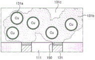
Fig. 3 is an enlarged sectional view illustrating a region a of fig. 2.
An enlarged view of a portion of the first external electrode 130 is shown in the region a, and a description about the first external electrode 130 will be provided hereinafter. However, since the configuration of the first external electrode 130 is similar to that of the second external electrode 140, this description may be considered to include the description of the second external electrode 140 as well, except that the first external electrode 130 is electrically connected to the first internal electrode 121 and the second external electrode 140 is connected to the second internal electrode 122.
As shown in fig. 3, the conductive resin layer 131 of the first external electrode 130 may include a plurality of metal particles 131a, a conductive connection portion 131b contacting the intermetallic compound 150, and a matrix resin 131 c.
The conductive resin layer 131 may serve to electrically and mechanically bond the intermetallic compound 150 and the first electrode layer 132 to each other. The conductive resin layer 131 can also prevent the generation of cracks when the multilayer capacitor 100 is mounted on a board by absorbing tensile stress generated in a mechanical or thermal environment at the time of mounting. The conductive resin layer 131 may also serve to protect the multilayer capacitor 100 from warpage impact associated with the board.
The conductive resin layer 131 may be formed by: a paste having a plurality of metal particles 131a dispersed in a matrix resin 131c is applied to the third surface 3 of the body 110, and then the paste is dried and hardened.
Unlike the external electrode formed by sintering according to the related art, the metal particles are not completely melted and may exist in a form in which the metal particles are randomly dispersed in the matrix resin 131c, and may be included in the conductive resin layer 131.
When the metal particles 131a react with the low melting point metal to form both the conductive connection part 131b and the intermetallic compound 150, the metal particles 131a may not be present in the conductive resin layer 131.
However, for convenience of explanation, a case where the metal particles 131a are present in the conductive resin layer 131 will be shown and described hereinafter in the present exemplary embodiment.
The metal particles 131a may include at least one selected from the group consisting of copper (Cu), nickel (Ni), silver (Ag), silver-coated copper (Cu), and tin (Sn-coated copper (Cu).
The metal particles 131a may have a size of 0.2 μm to 20 μm.
The metal particles included in the conductive resin layer 131 may be metal particles having a spherical shape, may be only metal particles 131a 'having a sheet shape as shown in fig. 4, or may be a mixed shape of metal particles 131a having a spherical shape and metal particles 131 a' having a sheet shape as shown in fig. 5.
The conductive connection part 131b may surround the plurality of metal particles 131a in a metal molten state to connect the plurality of metal particles 131a to each other, which may significantly reduce internal stress of the body 110 and may improve high temperature load (high temperature load) characteristics and humidity resistance load (humidity resistance load) characteristics.
The conductive connection part 131b may increase the conductivity of the conductive resin layer 131 to reduce the resistance of the conductive resin layer 131.
In the case where the metal particles 131a are included in the conductive resin layer 131, the conductive connection parts 131b may serve to increase connectivity between the metal particles 131a to further reduce the resistance of the conductive resin layer 131.
The low melting point metal included in the conductive connection part 131b may have a melting point lower than the hardening temperature of the base resin 131 c.
The low melting point metal included in the conductive connection part 131b may have a melting point of 300 deg.c or less.
The metal included In the conductive connection part 131b may be an alloy of two or more selected from the group consisting of tin (Sn), lead (Pb), indium (In), copper (Cu), silver (Ag), and bismuth (Bi).
In the case where the metal particles 131a are included in the conductive resin layer 131, the conductive connection part 131b may surround the plurality of metal particles 131a in a molten state to connect the plurality of metal particles 131a to each other.
Since the low melting point metal included in the conductive connection part 131b has a melting point lower than the hardening temperature of the base resin 131c, the low melting point metal may be melted in the drying and hardening process, and the conductive connection part 131b may cover the metal particles 131a in a melted state, as shown in fig. 3.
The conductive resin layer 131 may be formed by manufacturing a low melting point solder resin paste and then immersing the body in the low melting point solder resin paste. When silver or a metal coated with silver is used as a material of the metal particles 131a in manufacturing the low melting point solder resin paste, the conductive connection part 131b may include Ag3Sn。
The first and second internal electrodes 121 and 122 may include nickel (Ni), and the intermetallic compound 150 may include nickel-tin (Ni-Sn).
When a paste in which metal particles are dispersed is used as an electrode material, the flow of electrons is smooth where the metal particles contact each other, but rapidly decreases where the metal particles are surrounded by a matrix resin.
To solve this problem, the amount of the matrix resin may be significantly reduced and the amount of the metal particles may be increased to increase the contact ratio between the metal particles and improve the conductivity. However, the bonding strength of the external electrodes may be reduced due to the reduction in the amount of the matrix resin.
In the present exemplary embodiment, even without significantly reducing the amount of the thermosetting resin as the matrix resin, the contact ratio between the metal particles may be increased by the conductive connection portion, so that the adhesive strength of the external electrode may not be reduced and the conductivity in the conductive resin layer may be improved. Therefore, the Equivalent Series Resistance (ESR) of the multilayer capacitor can be reduced.
The intermetallic compound 150 may be disposed in the first groove portion and in contact with the conductive connection portion 131b to connect the first internal electrode 121 to the conductive connection portion 131 b. The exposed surface of the intermetallic compound 150 may form one substantially flat surface with the third surface 3 of the body. In another exemplary embodiment, the intermetallic compound 150 may also be formed in the conductive resin layer 131.
Accordingly, the intermetallic compound 150 may serve to improve electrical and mechanical bonding and reduce contact resistance between the conductive resin layer 131 and the first internal electrode 121 or between the conductive resin layer 141 and the second internal electrode 122.
The matrix resin 131c may include a thermosetting resin having an electrical insulating property.
The thermosetting resin may be, for example, an epoxy resin, but is not limited thereto.
The matrix resin 131c may serve to mechanically bond the main body 110 and the first electrode layer 132 to each other.
A second electrode layer may also be disposed on the first electrode layers 132 and 142.
The second electrode layer may be a plating layer, and may have, for example, a structure in which nickel (Ni) plating layers 133 and 143 and tin (Sn) plating layers 134 and 144 are sequentially stacked on the first electrode layers 132 and 142, respectively. The second electrode layer may also be formed using nickel or tin by a thin film deposition process such as Chemical Vapor Deposition (CVD), Physical Vapor Deposition (PVD), or the like.
Mechanism of forming A conductive resin layer
Fig. 6 is a diagram showing copper particles and tin/bismuth particles dispersed in an epoxy resin. Fig. 7 is a diagram illustrating that the oxide film of the copper particles is removed by an oxide film remover or heat. Fig. 8 is a diagram illustrating that the oxide film of the tin/bismuth particles is removed by an oxide film remover or heat. Fig. 9 is a diagram showing tin/bismuth particles melted to have fluidity. Fig. 10 is a diagram showing copper particles and tin/bismuth particles reacting with each other to form a copper-tin layer.
A mechanism for forming the conductive resin layer 131 will be described hereinafter with reference to fig. 6 to 10.
The conductive resin layer according to the present exemplary embodiment may include a plurality of metal particles, a low melting point metal, and a matrix resin. The metal particles may be nickel particles, silver-plated copper particles, tin particles, or tin-plated copper particles. In the present exemplary embodiment, copper particles are used as the metal particles as an example.
In the present exemplary embodiment, tin (Sn) -based solder may be used as the low melting point metal, and tin/bismuth (Sn/Bi) particles may be used as the low melting point metal. However, Sn-Pb, Sn-Cu, Sn-Ag-Cu, etc. may also be used as the low melting point metal. In the present exemplary embodiment, an epoxy resin is used as the matrix resin.
Referring to fig. 6 to 8, an epoxy resin used as the matrix resin 131c includes copper (Cu) particles 310 as metal particles having a high melting point and tin/bismuth (Sn/Bi) particles 410 as metal particles having a low melting point. The copper particles 310 and the tin-bismuth particles 410 may have oxide films 311 and 411, respectively, present on the surfaces thereof. The first internal electrode 121 may have an oxide film 121a present on a surface thereof.
The oxide films 311 and 411 may hinder the formation of a copper-tin layer by a reaction between the copper particles 310 and the tin/bismuth particles 410, and may be removed by an oxide film remover included in the epoxy resin or heat (Δ T) when performing a hardening process or by an acid solution treatment. The oxide film 121a of the first internal electrode 121 may also be removed.
The oxide film remover may be an acid, a base, a hydrogen halide, or the like, but is not limited thereto.
Referring to fig. 9 and 10, the tin/bismuth particles, of which the oxide film is removed, may start to melt at about 140 ℃. The molten tin/bismuth particles 412 may have fluidity and may move toward the copper particles 310 whose oxide film is removed. The melted tin/bismuth particles 412 may react with the copper particles 310 at a predetermined temperature to form the conductive connection part 131b, and may move toward the first groove part of the main body 110 where the first internal electrode 121 is exposed to form the intermetallic compound 150, and the intermetallic compound 150 is a copper-tin layer in the first groove part, as shown in fig. 10.
The intermetallic compound 150 formed as described above may be connected to the conductive connection part 131b of the conductive resin layer formed of copper-tin to reduce contact resistance between the first internal electrode 121 and the conductive resin layer.
The copper particle 131a shown in fig. 10 is a copper particle existing in the conductive connection portion 131b after the reaction as described above.
Surface oxidation may easily occur on the tin/bismuth particles 412 and may hinder the formation of the intermetallic compound 150. Thus, the tin/bismuth particles may be surface-treated so that the content of carbon is 1.0% to 60.5% to prevent surface oxidation.
The size of the metal particles for forming the intermetallic compound may be 0.2 μm to 20 μm. The metal particles may be one of nickel particles, silver-plated copper particles, tin-plated copper particles, and copper particles.
To form the intermetallic compound, the tin/bismuth particles melted to exist in a solution state at a predetermined temperature need to flow into the grooved portion of the main body and surround the metal particles. However, when the size of the metal particles exceeds 20 μm, the interval between the body and the metal particles may be too large, so that the tin/bismuth solution may not easily move between the groove portion of the body and the metal particles, thereby hindering the formation of intermetallic compounds.
In contrast, when the size of the metal particles is 20 μm or less, the distance between the metal particles may be reduced, and the tin/bismuth solution may move more easily to the recessed portion of the body due to capillary force generated in the region where the distance between the metal particles is reduced, so that intermetallic compounds may be easily formed.
However, when the size of the metal particles is less than 0.2 μm, oxidation may occur on the surface of the metal particles, which may hinder the formation of intermetallic compounds.
Further, in the present process, the melting temperature of the tin-bismuth particles and the formation temperature of the intermetallic compound need to be less than the hardening temperature of the epoxy resin as the matrix resin.
When the melting temperature of the tin-bismuth particles and the formation temperature of the intermetallic compound are higher than the hardening temperature of the epoxy resin, the matrix resin may be hardened first, so that the melted tin-bismuth particles may not move to the surface of the copper particles, and thus a copper-tin layer as the intermetallic compound may not be formed.
The content of the tin-bismuth particles for forming the intermetallic compound may be 10 wt% to 90 wt% with respect to the total metal particles.
When the content of the tin-bismuth particles is less than 10 wt%, the size of the intermetallic compound formed by the reaction between the tin-bismuth particles and the metal particles may be excessively increased, so that it may be difficult to form the intermetallic compound in the groove portion of the main body and it may be difficult to provide the conductive connection portion on the third surface or the fourth surface of the main body.
When the content of the tin-bismuth particles exceeds 90 wt%, the tin-bismuth particles may react with each other, so that only the size of the tin-bismuth particles may be increased without forming an intermetallic compound.
Furthermore, it may be desirable to adjust the tin content of the tin-bismuth particles.
In the present exemplary embodiment, the component that reacts with the metal particles to form the intermetallic compound may be tin, and thus Snx-BiyThe content (x) of Sn in (b) may be 10 wt% or more with respect to the total metal particles to ensure a predetermined level or more of reactivity.
When the content (x) of Sn is less than 10 wt% with respect to the total metal particles, ESR of the manufactured multilayer capacitor may be increased.
In a multilayer capacitor using a conductive resin layer in an external electrode thereof, ESR may be affected by various resistance components applied to the external electrode.
These resistance components may include the resistance of the internal electrode, the contact resistance between the conductive resin layer and the internal electrode, the resistance of the conductive resin layer, the contact resistance between the first electrode layer and the conductive resin layer, and the resistance of the first electrode layer.
The resistance of the internal electrode and the resistance of the first electrode layer are fixed values and do not change.
According to the present exemplary embodiment, the sintered electrode layer does not exist between the external electrode and the body to solve the problem that the sintered electrode layer generates bending stress when the sheet is bent according to the related art. In addition, the process temperature may be reduced to prevent cracks from being generated in the body.
The bonding strength of the external electrodes may be increased by the intermetallic compound to further improve the warpage strength of the multilayer capacitor, as compared to the electrode layer having sintering in the outermost side of the external electrodes.
In addition, the electrical connectivity between the internal electrodes and the conductive resin layer may be improved by the intermetallic compound. Therefore, the contact resistance can be reduced to further reduce the ESR of the multilayer capacitor.
The external electrode of the multilayer capacitor according to the related art has the following structure: copper (Cu) paste is applied to both end surfaces of the main body exposing the internal electrodes, and then sintered to form electrode layers. Then, a nickel (Ni) plating layer is formed on the electrode layer to prevent the solder from dissolving, and a tin (Sn) plating layer is formed on the nickel plating layer to improve wettability of the solder when the chip board is present on the nickel plating layer.
In that case, the nickel plating layer may prevent external moisture from penetrating into the tin plating layer, but may not sufficiently prevent penetration of the plating solution or moisture due to small defects of the nickel plating layer.
In the multilayer capacitor according to the present exemplary embodiment, the primary external electrode is formed using a low melting point metal resin that is very resistant to the penetration of a plating solution and moisture.
Since the internal electrode (e.g., Ni electrode) and the intermetallic compound ("IMC") are formed in a low-temperature hardening process using a low-melting metal, the low-melting metal resin electrode may have excellent electrical connectivity.
The IMC may be formed in the low melting point metal resin electrode to suppress penetration of the plating solution and external moisture.
A copper (Cu) electrode layer is formed as a secondary external electrode through a plating process to further improve the characteristics of preventing penetration of a plating solution and moisture.
Since the copper electrode layer formed by plating has a high electrode density, the copper electrode layer can further improve the property of preventing penetration of a plating solution and moisture, compared to a sintered copper electrode layer.
Then, a nickel (Ni) plating layer may be formed to prevent the solder from dissolving, and a tin (Sn) plating layer may be formed to improve wettability of the solder.
Since the process of forming the external electrode as described above may be performed at a temperature of 250 deg.c or less, a waterproof coating process for preventing moisture from penetrating may be used.
Since the thickness of the primary external electrode, which is a low melting point metal resin electrode, can be reduced due to improved characteristics of preventing penetration of a plating solution and external moisture, the effective area and capacitance of the chip can be increased, compared to the existing sintered Cu electrode.
According to the present exemplary embodiment, the primary electrode layer of the external electrode may be a low melting point metal resin layer, the secondary electrode layer of the external electrode may be a copper electrode layer, the tertiary electrode layer of the external electrode may be a nickel electrode layer, and the quaternary electrode layer of the external electrode may be a tin electrode layer.
Modified examples
Referring to fig. 11, a multilayer capacitor 100' according to another exemplary embodiment of the present disclosure may include moisture permeation prevention layers 161 and 162 formed at first and second surfaces 1 and 2 of a body 110, respectively.
In order to avoid repetitive description, detailed description of a structure similar to that of the multilayer capacitor according to the above-described exemplary embodiment will be omitted. The moisture permeation prevention layers 161 and 162 corresponding to a structure different from that of the multilayer capacitor according to the above-described exemplary embodiment will be shown and described in detail.
The moisture permeation prevention layers 161 and 162 may be made of parylene, Al2O3、SiO2Etc. formed organic or inorganic layers. The moisture permeation prevention layers 161 and 162 may be formed by dipping, coating, and using a thin film deposition process such as Chemical Vapor Deposition (CVD)/Physical Vapor Deposition (PVD), Atomic Layer Deposition (ALD), and the like.
In the present exemplary embodiment, the conductive resin layer is formed as an internal layer in contact with the third surface 3 and the fourth surface 4 of the body 110, and a low melting point metal on which a process may be performed at a low temperature is used as a material of the conductive resin layer, so that an organic layer, which may not be used at a high process temperature, may be used as a moisture permeation prevention layer.
The moisture penetration preventing layers 161 and 162 may significantly improve the reliability of the multilayer capacitor.
Method for manufacturing multilayer capacitor
Hereinafter, a method of manufacturing a multilayer capacitor according to an exemplary embodiment of the present disclosure will be described in detail, but the present disclosure is not limited thereto, and a repetitive description will be omitted.
In the method of manufacturing the multilayer capacitor according to the present exemplary embodiment, a material such as barium titanate (BaTiO) may be included3) A slurry of powder such as powder is applied to a carrier film and dried to prepare a plurality of ceramic green sheets, thereby forming a dielectric layer and a cap.
The ceramic green sheet can be manufactured by preparing a slurry by mixing ceramic powder, a binder and a solvent together and manufacturing the slurry into a sheet shape having a thickness of several micrometers by a doctor blade method.
The internal electrodes can be formed by applying a conductive paste for internal electrodes including a conductive metal such as copper to the ceramic green sheets by a screen printing method or the like.
A plurality of ceramic green sheets on which internal electrodes are printed may be stacked to form a stacked body, and a plurality of ceramic green sheets on which internal electrodes are not printed may be stacked on upper and lower surfaces of the stacked body and then sintered to prepare a main body. The internal electrodes may include first and second internal electrodes having different polarities.
That is, the body may include a dielectric layer, first and second internal electrodes, and a cover. The dielectric layer may be formed by sintering the ceramic green sheets on which the internal electrodes are printed, and the cap may be formed by sintering the ceramic green sheets without the internal electrodes.
The body may have first and second surfaces facing away from each other, third and fourth surfaces connected to the first and second surfaces and facing away from each other, and fifth and sixth surfaces facing away from each other, connected to the first and second surfaces, and connected to the third and fourth surfaces, and may include a plurality of first groove portions and a plurality of second groove portions formed between the dielectric layers in the third and fourth surfaces, respectively. The dielectric layer may be perpendicular to the third and fourth surfaces such that ends of the first and second internal electrodes are exposed to respective sides of the body.
A conductive resin composite including metal particles, a thermosetting resin, and a low-melting metal having a melting point lower than that of the thermosetting resin can be prepared.
The conductive resin composite can be prepared by mixing together, for example, copper particles as metal particles, tin/bismuth particles as a low-melting metal, an oxide film remover, and 4 to 15 wt% of an epoxy resin, and then dispersing them using a three-roll mill.
The conductive resin composite may be applied to the third and fourth surfaces of the body and then dried and hardened to form a conductive resin layer having a conductive connection portion surrounding the melted low melting point metal.
When the conductive resin layer is formed, the oxide film on the surfaces of the metal particles and the low melting point metal in the thermosetting resin can be removed. The metal particles whose oxide film is removed and the low melting point metal may react with each other to form the conductive connection portion. The low melting point metal may have fluidity to flow into the first groove portion and the second groove portion of the body, thereby forming an intermetallic compound in the first groove portion and the second groove portion, which is in contact with the end portions of the first internal electrode and the second internal electrode and is formed of copper-tin or the like.
When some of the metal particles do not completely react with the low melting point metal so that they remain, the remaining metal particles may exist in the conductive resin layer covered with the melted low melting point metal.
The metal particles may include at least one selected from the group consisting of copper, nickel, silver-coated copper, and tin-coated copper, but are not limited thereto.
The low melting point metal may be at least one selected from the group consisting of Sn/Bi, Sn-Pb, Sn-Cu, Sn-Ag, and Sn-Ag-Cu, but is not limited thereto.
The thermosetting resin may include an epoxy resin, but is not limited thereto, and may be, for example, a bisphenol a resin, a glycol epoxy resin, a novolac epoxy resin, or a resin in a liquid state at room temperature due to a small molecular weight in its derivative.
A first electrode layer electrically connected to the conductive resin layer may be formed on the conductive resin layer.
The first electrode layer may be formed by applying and then sintering a paste including a conductive metal and glass.
The conductive metal is not particularly limited, but may be, for example, one or more selected from the group consisting of copper, nickel, palladium, gold, silver, and alloys thereof.
The glass is not particularly limited, but may be a material having the same composition as that of the glass used for manufacturing the external electrodes of the existing multilayer capacitor.
A second electrode layer may also be formed on the first electrode layer. The second electrode layer may be formed by plating, and may include, for example, a nickel plating layer and a tin plating layer further formed on the nickel plating layer.
The moisture permeation prevention layers may be formed on the first surface and the second surface of the body, respectively, before applying the conductive resin composition to the body.
As described above, according to exemplary embodiments of the present disclosure, a predetermined level of capacitance of a multilayer capacitor may be ensured, and the multilayer capacitor may have reduced ESR, improved warp strength, and improved reliability.
While exemplary embodiments have been shown and described above, it will be apparent to those skilled in the art that modifications and variations can be made without departing from the scope of the invention as defined by the appended claims.
Claims (39)
1. A multilayer capacitor, comprising:
a body including a plurality of first and second internal electrodes alternately stacked with a dielectric layer interposed therebetween, the body has first and second surfaces facing away from each other, third and fourth surfaces facing away from each other and connected to the first and second surfaces, and fifth and sixth surfaces facing away from each other, connected to the first and second surfaces and connected to the third and fourth surfaces, and the body includes a plurality of first groove portions and a plurality of second groove portions between the dielectric layers in the third and fourth surfaces, wherein the dielectric layer is perpendicular to the third surface and the fourth surface, and end portions of the first internal electrode and the second internal electrode are exposed from the body through the first recess portion and the second recess portion, respectively;
an intermetallic compound located in the first groove portion and the second groove portion and connected to the end portions of the first internal electrode and the second internal electrode, respectively; and
first and second external electrodes on the third and fourth surfaces of the body, respectively,
wherein the first and second external electrodes include:
a conductive resin layer provided on the third surface and the fourth surface of the body, respectively, and including a plurality of metal particles, a conductive connection portion surrounding the plurality of metal particles and in contact with the intermetallic compound, and a matrix resin; and
the first electrode layer is positioned on the corresponding conductive resin layer and is in contact with the conductive connecting part, and the first electrode layer is a copper plating layer;
wherein the first and second external electrodes further include second electrode layers on the first electrode layers, respectively, the second electrode layers each including a nickel plating layer and a tin plating layer sequentially stacked on the first electrode layers,
wherein the conductive connection portion continuously extends from the first electrode layer to the intermetallic compound and is integrally connected with the intermetallic compound.
2. The multilayer capacitor of claim 1, wherein the conductive connection portion comprises a material having a melting point lower than a hardening temperature of the matrix resin.
3. The multilayer capacitor of claim 2, wherein the material of the conductive connection has a melting point of 300 ℃ or less.
4. The multilayer capacitor of claim 1, wherein the conductive connection comprises an alloy of two or more materials from the group consisting of tin, lead, indium, copper, silver, and bismuth.
5. The multilayer capacitor of claim 1, wherein the metal particles of the conductive resin layer comprise at least one material from the group consisting of copper, nickel, silver-coated copper, and tin-coated copper.
6. The multilayer capacitor of claim 1, wherein the internal electrode comprises nickel and the intermetallic compound comprises nickel-tin.
7. The multilayer capacitor of claim 1, wherein the internal electrode comprises one material from the group consisting of nickel, copper, and palladium, or an alloy thereof.
8. The multilayer capacitor as claimed in claim 1, wherein the metal particles of the conductive resin layer have a spherical shape, a sheet shape, or a mixed shape of a spherical shape and a sheet shape.
9. The multilayer capacitor as claimed in claim 1, wherein the conductive resin layers of the first and second external electrodes include connection portions on the third and fourth surfaces of the body, respectively, and include band portions extending from the connection portions to the first, second, fifth and sixth surfaces of the body, respectively.
10. The multilayer capacitor of claim 1, wherein the body further comprises upper and lower caps respectively above and below the plurality of first and second internal electrodes, the upper and lower caps comprising the same material as the dielectric layer.
11. The multilayer capacitor as claimed in claim 1, further comprising moisture permeation prevention layers respectively formed on the first and second surfaces of the body.
12. A multilayer capacitor, comprising:
a body including a plurality of first and second internal electrodes alternately stacked with a dielectric layer interposed therebetween, the body having first and second surfaces facing away from each other, third and fourth surfaces facing away from each other and connected to the first and second surfaces, and fifth and sixth surfaces facing away from each other and connected to the first and second surfaces, wherein ends of the first and second internal electrodes are exposed from the body at the third and fourth surfaces, respectively;
an intermetallic compound connected to the end portions of the first and second internal electrodes, respectively;
a moisture permeation prevention layer on the first surface and the second surface of the body, respectively; and
first and second external electrodes on the third and fourth surfaces of the body, respectively,
wherein the first and second external electrodes include:
a conductive resin layer respectively on the third surface and the fourth surface of the body and including a plurality of metal particles, a conductive connection portion surrounding the plurality of metal particles and contacting the intermetallic compound, and a matrix resin; and
a first electrode layer on the corresponding conductive resin layer and in contact with the conductive connection part, the first electrode layer being a copper plating layer,
wherein the first and second external electrodes further include second electrode layers on the first electrode layers, respectively, the second electrode layers each including a nickel plating layer and a tin plating layer sequentially stacked on the first electrode layers,
wherein the conductive connection portion continuously extends from the first electrode layer to the intermetallic compound and is integrally connected with the intermetallic compound.
13. The multilayer capacitor of claim 12, wherein the conductive connection comprises a material having a melting point lower than a hardening temperature of the matrix resin.
14. The multilayer capacitor of claim 13, wherein the material of the conductive connection has a melting point of 300 ℃ or less.
15. The multilayer capacitor of claim 12, wherein the conductive connection comprises an alloy of two or more materials from the group consisting of tin, lead, indium, copper, silver, and bismuth.
16. The multilayer capacitor of claim 12, wherein the metal particles of the conductive resin layer comprise at least one material from the group consisting of copper, nickel, silver-coated copper, and tin-coated copper.
17. The multilayer capacitor of claim 12, wherein the internal electrode comprises nickel and the intermetallic compound comprises nickel-tin.
18. The multilayer capacitor of claim 12, wherein the internal electrode comprises one material from the group consisting of nickel, copper, and palladium, or an alloy thereof.
19. The multilayer capacitor as claimed in claim 12, wherein the metal particles of the conductive resin layer have a spherical shape, a sheet shape, or a mixed shape of a spherical shape and a sheet shape.
20. The multilayer capacitor according to claim 12, wherein the conductive resin layers of the first and second external electrodes include connection portions on the third and fourth surfaces of the body, respectively, and include band portions extending from the connection portions to the first, second, fifth, and sixth surfaces of the body, respectively.
21. The multilayer capacitor of claim 12, wherein the body further comprises upper and lower caps respectively above and below the plurality of first and second internal electrodes, the upper and lower caps comprising the same material as the dielectric layer.
22. A multilayer capacitor, comprising:
a body including a plurality of first and second internal electrodes alternately stacked with a dielectric layer interposed therebetween, the body having first and second surfaces facing away from each other, third and fourth surfaces facing away from each other and connected to the first and second surfaces, and fifth and sixth surfaces facing away from each other and connected to the first and second surfaces, wherein ends of the first and second internal electrodes are exposed from the body at the third and fourth surfaces, respectively;
an intermetallic compound connected to the end portions of the first and second internal electrodes, respectively; and
first and second external electrodes on the third and fourth surfaces of the body, respectively,
wherein the first and second external electrodes include:
a conductive resin layer respectively on the third surface and the fourth surface of the body and including a plurality of metal particles, a conductive connection portion surrounding the plurality of metal particles and contacting the intermetallic compound, and a matrix resin; and
first electrode layers on the respective conductive resin layers and in contact with the conductive connection parts, and
the first electrode layer is a copper plating layer,
wherein the first and second external electrodes further include second electrode layers on the first electrode layers, respectively, the second electrode layers each including a nickel plating layer and a tin plating layer sequentially stacked on the first electrode layers,
wherein the conductive connection portion continuously extends from the first electrode layer to the intermetallic compound and is integrally connected with the intermetallic compound.
23. The multilayer capacitor of claim 22, wherein the conductive connection comprises a material having a melting point lower than a hardening temperature of the matrix resin.
24. The multilayer capacitor of claim 23, wherein the material of the conductive connection has a melting point of 300 ℃ or less.
25. The multilayer capacitor of claim 22, wherein the conductive connection comprises an alloy of two or more materials from the group consisting of tin, lead, indium, copper, silver, and bismuth.
26. The multilayer capacitor of claim 22, wherein the metal particles of the conductive resin layer comprise at least one material from the group consisting of copper, nickel, silver-coated copper, and tin-coated copper.
27. The multilayer capacitor of claim 22, wherein the internal electrode comprises nickel and the intermetallic compound comprises nickel-tin.
28. The multilayer capacitor of claim 22, wherein the internal electrode comprises a material from the group consisting of nickel, copper, and palladium, or alloys thereof.
29. The multilayer capacitor of claim 22, wherein the metal particles of the conductive resin layer have a spherical shape, a sheet shape, or a mixed shape of a spherical shape and a sheet shape.
30. The multilayer capacitor as claimed in claim 22, the first and second external electrodes respectively include connection portions on the third and fourth surfaces of the body, and respectively include band portions extending from the connection portions to the first, second, fifth and sixth surfaces of the body.
31. The multilayer capacitor of claim 22, wherein the body further comprises upper and lower caps respectively above and below the plurality of first and second internal electrodes, the upper and lower caps comprising the same material as the dielectric layer.
32. A multilayer capacitor, comprising:
a body including a plurality of internal electrodes, wherein the plurality of internal electrodes are exposed from the body through a plurality of recess portions in first and second surfaces of the body facing away from each other;
an external electrode electrically connected to the plurality of internal electrodes and including conductive resin layers on the first and second surfaces of the body and a first electrode layer on the conductive resin layer, the first electrode layer being a copper plating layer,
wherein the main body includes an intermetallic compound in a plurality of the groove portions and in contact with the respective plurality of internal electrodes, and
wherein the conductive resin layer includes a base resin and a conductive connection portion electrically connecting the first electrode layer to the intermetallic compound in the plurality of groove portions,
wherein the external electrode further comprises a second electrode layer on the first electrode layer, the second electrode layer comprising a nickel plating layer and a tin plating layer sequentially stacked on the first electrode layer,
wherein the conductive connection portion continuously extends from the first electrode layer to the intermetallic compound and is integrally connected with the intermetallic compound.
33. The multilayer capacitor as in claim 32,
wherein the conductive resin layer of the external electrode further includes a plurality of metal particles, and
wherein the conductive connection portion surrounds the plurality of metal particles.
34. The multilayer capacitor of claim 32, wherein the conductive connection comprises a material having a melting point lower than a hardening temperature of the matrix resin.
35. The multilayer capacitor of claim 32, further comprising moisture permeation prevention layers respectively on third and fourth surfaces of the body that face away from each other, both the third and fourth surfaces being connected to the first and second surfaces of the body.
36. A method of manufacturing a multilayer capacitor comprising the steps of;
forming a body by stacking a plurality of ceramic green sheets on which internal electrodes are printed and stacking a plurality of ceramic green sheets on which internal electrodes are not printed on upper and lower surfaces of the stacked body and sintering, the body having a plurality of groove portions formed in first and second surfaces thereof facing away from each other;
applying a conductive resin composite onto third and fourth surfaces of the body facing away from each other, the conductive resin composite including first metal particles covered with an oxide film, second metal particles including a low melting point metal and covered with an oxide film, and a base resin;
removing the oxide film of the first metal particles and the oxide film of the second metal particles;
hardening the conductive resin composite to form a conductive resin layer in which second metal particles are melted and reacted with the first metal particles to form conductive connection portions that flow within the base resin and into the plurality of groove portions to form an intermetallic compound that is in contact with the end portions of the internal electrodes;
forming a first electrode layer on the conductive resin layer, wherein the first electrode layer is a copper plating layer;
forming a second electrode layer on the first electrode layer, the second electrode layer including a nickel plating layer and a tin plating layer sequentially stacked on the first electrode layer,
wherein the conductive connection portion continuously extends from the first electrode layer to the intermetallic compound and is integrally connected with the intermetallic compound.
37. A method of manufacturing a multilayer capacitor according to claim 36, wherein the second metal particles have a size in the range of 0.2 μm to 20 μm.
38. The method for manufacturing a multilayer capacitor as claimed in claim 36, wherein the melting point of the low melting point metal is 300 ℃ or less, and the hardening temperature of the matrix resin is higher than the melting point of the low melting point metal.
39. A multilayer capacitor, comprising:
a body including a plurality of first and second internal electrodes alternately stacked with a dielectric layer interposed therebetween, the body has first and second surfaces facing away from each other, third and fourth surfaces facing away from each other and connected to the first and second surfaces, and fifth and sixth surfaces facing away from each other, connected to the first and second surfaces and connected to the third and fourth surfaces, and the body includes a plurality of first groove portions and a plurality of second groove portions between the dielectric layers in the third and fourth surfaces, wherein the dielectric layer is perpendicular to the third surface and the fourth surface, and end portions of the first internal electrode and the second internal electrode are exposed from the body through the first recess portion and the second recess portion, respectively;
an intermetallic compound located in the first groove portion and the second groove portion and connected to the end portions of the first internal electrode and the second internal electrode, respectively;
moisture permeation prevention layers formed on the first surface and the second surface of the body, respectively; and
first and second external electrodes on the third and fourth surfaces of the body, respectively, and extending onto the first and second surfaces to cover ends of the moisture permeation prevention layer,
wherein the first and second external electrodes include:
a conductive resin layer respectively provided on the third surface and the fourth surface of the body, extending onto the first surface and the second surface, and including a plurality of metal particles, a conductive connection portion surrounding the plurality of metal particles and contacting the intermetallic compound, and a matrix resin; and
a first electrode layer on the corresponding conductive resin layer and in contact with the conductive connection part, the first electrode layer being a copper plating layer,
wherein both ends of the moisture permeation prevention layer are disposed to be sandwiched between the conductive resin layer and the first surface or the second surface of the body,
wherein the conductive connection portion continuously extends from the first electrode layer to the intermetallic compound and is integrally connected with the intermetallic compound.
Applications Claiming Priority (4)
| Application Number | Priority Date | Filing Date | Title |
|---|---|---|---|
| KR20170043494 | 2017-04-04 | ||
| KR10-2017-0043494 | 2017-04-04 | ||
| KR10-2017-0053082 | 2017-04-25 | ||
| KR1020170053082A KR101922879B1 (en) | 2017-04-04 | 2017-04-25 | Multilayered capacitor |
Publications (2)
| Publication Number | Publication Date |
|---|---|
| CN108695067A CN108695067A (en) | 2018-10-23 |
| CN108695067B true CN108695067B (en) | 2022-01-07 |
Family
ID=63876580
Family Applications (1)
| Application Number | Title | Priority Date | Filing Date |
|---|---|---|---|
| CN201710821519.XA Active CN108695067B (en) | 2017-04-04 | 2017-09-13 | Multilayer capacitor and method for manufacturing multilayer capacitor |
Country Status (3)
| Country | Link |
|---|---|
| JP (2) | JP2018182274A (en) |
| KR (2) | KR101922879B1 (en) |
| CN (1) | CN108695067B (en) |
Families Citing this family (15)
| Publication number | Priority date | Publication date | Assignee | Title |
|---|---|---|---|---|
| JP7053095B2 (en) * | 2018-11-29 | 2022-04-12 | サムソン エレクトロ-メカニックス カンパニーリミテッド. | Multilayer ceramic capacitors |
| JP2020107705A (en) * | 2018-12-27 | 2020-07-09 | Tdk株式会社 | Electronic component |
| JP7276646B2 (en) * | 2019-02-01 | 2023-05-18 | Tdk株式会社 | ceramic electronic components |
| KR102211744B1 (en) * | 2019-02-21 | 2021-02-04 | 삼성전기주식회사 | Multilayered capacitor |
| US11183331B2 (en) * | 2019-02-21 | 2021-11-23 | Samsung Electro-Mechanics Co., Ltd. | MLCC module and method of manufacturing the same |
| JP7226161B2 (en) | 2019-07-17 | 2023-02-21 | 株式会社村田製作所 | electronic components |
| JP7088134B2 (en) | 2019-07-17 | 2022-06-21 | 株式会社村田製作所 | Electronic components |
| KR102270303B1 (en) * | 2019-08-23 | 2021-06-30 | 삼성전기주식회사 | Multilayered capacitor and board having the same mounted thereon |
| KR102276514B1 (en) * | 2019-08-28 | 2021-07-14 | 삼성전기주식회사 | Mutilayered electronic component |
| KR20190116181A (en) | 2019-09-20 | 2019-10-14 | 삼성전기주식회사 | Multilayered electronic component |
| JP2021136323A (en) | 2020-02-27 | 2021-09-13 | 株式会社村田製作所 | Multilayer ceramic electronic component |
| JP7314884B2 (en) | 2020-08-31 | 2023-07-26 | 株式会社村田製作所 | Laminated ceramic electronic component and manufacturing method thereof |
| JP7396251B2 (en) | 2020-11-11 | 2023-12-12 | 株式会社村田製作所 | multilayer ceramic capacitor |
| CN116918015A (en) * | 2021-03-31 | 2023-10-20 | 株式会社村田制作所 | Laminated ceramic capacitor |
| KR20230068722A (en) * | 2021-11-11 | 2023-05-18 | 삼성전기주식회사 | Composite electronic component |
Citations (4)
| Publication number | Priority date | Publication date | Assignee | Title |
|---|---|---|---|---|
| JPH09260199A (en) * | 1996-03-25 | 1997-10-03 | Taiyo Yuden Co Ltd | Multilayer capacitor |
| CN1723514A (en) * | 2002-12-09 | 2006-01-18 | 松下电器产业株式会社 | Electronic part with external electrode |
| CN201196910Y (en) * | 2008-05-29 | 2009-02-18 | 成都宏明电子股份有限公司 | Packaging body used for sheet-type multilayer ceramic capacitor and sheet-type multi-layer piezoresistor |
| CN101587774A (en) * | 2008-05-21 | 2009-11-25 | 株式会社村田制作所 | Laminated electronic component and method for manufacturing the same |
Family Cites Families (15)
| Publication number | Priority date | Publication date | Assignee | Title |
|---|---|---|---|---|
| US3532014A (en) | 1968-10-01 | 1970-10-06 | Norman C Franz | Method for the high velocity liquid jet cutting of soft materials |
| US5750264A (en) * | 1994-10-19 | 1998-05-12 | Matsushita Electric Industrial Co., Inc. | Electronic component and method for fabricating the same |
| EP0777242A3 (en) * | 1995-11-29 | 1999-12-01 | Matsushita Electric Industrial Co., Ltd | A ceramic electronic component and its manufacturing method |
| JPH10144504A (en) * | 1996-11-06 | 1998-05-29 | Mitsubishi Materials Corp | Chip-type thermistor and its manufacture |
| JP3531543B2 (en) * | 1999-07-30 | 2004-05-31 | 株式会社村田製作所 | Manufacturing method of multilayer ceramic electronic component and multilayer ceramic electronic component |
| US6627509B2 (en) * | 2001-11-26 | 2003-09-30 | Delaware Capital Formation, Inc. | Surface flashover resistant capacitors and method for producing same |
| JP4901078B2 (en) | 2003-07-15 | 2012-03-21 | 株式会社村田製作所 | Chip electronic components |
| KR101018240B1 (en) * | 2008-08-12 | 2011-03-03 | 삼성전기주식회사 | Multi-layered ceramic capacitor and manufacturing method of the same |
| JP5439944B2 (en) * | 2009-05-18 | 2014-03-12 | 株式会社村田製作所 | Multilayer electronic component and manufacturing method thereof |
| KR20130049296A (en) * | 2011-11-04 | 2013-05-14 | 삼성전기주식회사 | Method for manufacturing multi-layer ceramic electronic parts |
| KR101635133B1 (en) * | 2012-01-23 | 2016-06-30 | 가부시키가이샤 무라타 세이사쿠쇼 | Electronic part and manufacturing method therefor |
| JP2015026815A (en) * | 2013-06-19 | 2015-02-05 | 株式会社村田製作所 | Ceramic electronic component and method of manufacturing the same |
| KR20150089276A (en) * | 2014-01-27 | 2015-08-05 | 삼성전기주식회사 | Multi-layered ceramic electronic part and conductive paste for external electrode |
| KR101630050B1 (en) * | 2014-07-25 | 2016-06-13 | 삼성전기주식회사 | Multi-layered ceramic electronic part |
| KR101975133B1 (en) * | 2015-01-30 | 2019-05-03 | 가부시키가이샤 무라타 세이사쿠쇼 | METHOD FOR MANUFACTURING ELECTRONIC COMPONENTS |
-
2017
- 2017-04-25 KR KR1020170053082A patent/KR101922879B1/en active IP Right Grant
- 2017-07-25 JP JP2017144018A patent/JP2018182274A/en active Pending
- 2017-09-13 CN CN201710821519.XA patent/CN108695067B/en active Active
-
2018
- 2018-07-10 KR KR1020180080199A patent/KR102212642B1/en active IP Right Grant
-
2019
- 2019-03-19 JP JP2019051275A patent/JP7176814B2/en active Active
Patent Citations (4)
| Publication number | Priority date | Publication date | Assignee | Title |
|---|---|---|---|---|
| JPH09260199A (en) * | 1996-03-25 | 1997-10-03 | Taiyo Yuden Co Ltd | Multilayer capacitor |
| CN1723514A (en) * | 2002-12-09 | 2006-01-18 | 松下电器产业株式会社 | Electronic part with external electrode |
| CN101587774A (en) * | 2008-05-21 | 2009-11-25 | 株式会社村田制作所 | Laminated electronic component and method for manufacturing the same |
| CN201196910Y (en) * | 2008-05-29 | 2009-02-18 | 成都宏明电子股份有限公司 | Packaging body used for sheet-type multilayer ceramic capacitor and sheet-type multi-layer piezoresistor |
Also Published As
| Publication number | Publication date |
|---|---|
| KR102212642B1 (en) | 2021-02-08 |
| KR20180112643A (en) | 2018-10-12 |
| JP2018182274A (en) | 2018-11-15 |
| KR20180112732A (en) | 2018-10-12 |
| JP2019117942A (en) | 2019-07-18 |
| JP7176814B2 (en) | 2022-11-22 |
| KR101922879B1 (en) | 2018-11-29 |
| CN108695067A (en) | 2018-10-23 |
Similar Documents
| Publication | Publication Date | Title |
|---|---|---|
| CN108695067B (en) | Multilayer capacitor and method for manufacturing multilayer capacitor | |
| US10770234B2 (en) | Multilayer capacitor | |
| US11342119B2 (en) | Multilayer capacitor having external electrode including conductive resin layer | |
| US20190295773A1 (en) | Multilayer capacitor having external electrode including conductive resin layer | |
| CN112133559A (en) | Multilayer ceramic electronic component and method for manufacturing same | |
| CN109216022B (en) | Multilayer ceramic capacitor, method for manufacturing the same, and electronic component | |
| CN111243864B (en) | Multilayer ceramic capacitor | |
| US11817267B2 (en) | Multilayer capacitor | |
| US20230197344A1 (en) | Multilayer electronic component | |
| US11804332B2 (en) | Multilayered electronic component | |
| CN115881433A (en) | Capacitor assembly |
Legal Events
| Date | Code | Title | Description |
|---|---|---|---|
| PB01 | Publication | ||
| PB01 | Publication | ||
| SE01 | Entry into force of request for substantive examination | ||
| SE01 | Entry into force of request for substantive examination | ||
| GR01 | Patent grant | ||
| GR01 | Patent grant |