CN108539440B - Anisotropic conductive film and connection structure - Google Patents
Anisotropic conductive film and connection structure Download PDFInfo
- Publication number
- CN108539440B CN108539440B CN201810229524.6A CN201810229524A CN108539440B CN 108539440 B CN108539440 B CN 108539440B CN 201810229524 A CN201810229524 A CN 201810229524A CN 108539440 B CN108539440 B CN 108539440B
- Authority
- CN
- China
- Prior art keywords
- center
- electronic component
- conductive particles
- conductive film
- anisotropic conductive
- Prior art date
- Legal status (The legal status is an assumption and is not a legal conclusion. Google has not performed a legal analysis and makes no representation as to the accuracy of the status listed.)
- Active
Links
Images

Classifications
-
- H—ELECTRICITY
- H01—ELECTRIC ELEMENTS
- H01L—SEMICONDUCTOR DEVICES NOT COVERED BY CLASS H10
- H01L24/00—Arrangements for connecting or disconnecting semiconductor or solid-state bodies; Methods or apparatus related thereto
- H01L24/80—Methods for connecting semiconductor or other solid state bodies using means for bonding being attached to, or being formed on, the surface to be connected
- H01L24/83—Methods for connecting semiconductor or other solid state bodies using means for bonding being attached to, or being formed on, the surface to be connected using a layer connector
-
- H—ELECTRICITY
- H01—ELECTRIC ELEMENTS
- H01B—CABLES; CONDUCTORS; INSULATORS; SELECTION OF MATERIALS FOR THEIR CONDUCTIVE, INSULATING OR DIELECTRIC PROPERTIES
- H01B5/00—Non-insulated conductors or conductive bodies characterised by their form
- H01B5/16—Non-insulated conductors or conductive bodies characterised by their form comprising conductive material in insulating or poorly conductive material, e.g. conductive rubber
-
- C—CHEMISTRY; METALLURGY
- C09—DYES; PAINTS; POLISHES; NATURAL RESINS; ADHESIVES; COMPOSITIONS NOT OTHERWISE PROVIDED FOR; APPLICATIONS OF MATERIALS NOT OTHERWISE PROVIDED FOR
- C09J—ADHESIVES; NON-MECHANICAL ASPECTS OF ADHESIVE PROCESSES IN GENERAL; ADHESIVE PROCESSES NOT PROVIDED FOR ELSEWHERE; USE OF MATERIALS AS ADHESIVES
- C09J7/00—Adhesives in the form of films or foils
- C09J7/10—Adhesives in the form of films or foils without carriers
-
- C—CHEMISTRY; METALLURGY
- C09—DYES; PAINTS; POLISHES; NATURAL RESINS; ADHESIVES; COMPOSITIONS NOT OTHERWISE PROVIDED FOR; APPLICATIONS OF MATERIALS NOT OTHERWISE PROVIDED FOR
- C09J—ADHESIVES; NON-MECHANICAL ASPECTS OF ADHESIVE PROCESSES IN GENERAL; ADHESIVE PROCESSES NOT PROVIDED FOR ELSEWHERE; USE OF MATERIALS AS ADHESIVES
- C09J7/00—Adhesives in the form of films or foils
- C09J7/20—Adhesives in the form of films or foils characterised by their carriers
-
- C—CHEMISTRY; METALLURGY
- C09—DYES; PAINTS; POLISHES; NATURAL RESINS; ADHESIVES; COMPOSITIONS NOT OTHERWISE PROVIDED FOR; APPLICATIONS OF MATERIALS NOT OTHERWISE PROVIDED FOR
- C09J—ADHESIVES; NON-MECHANICAL ASPECTS OF ADHESIVE PROCESSES IN GENERAL; ADHESIVE PROCESSES NOT PROVIDED FOR ELSEWHERE; USE OF MATERIALS AS ADHESIVES
- C09J9/00—Adhesives characterised by their physical nature or the effects produced, e.g. glue sticks
- C09J9/02—Electrically-conducting adhesives
-
- H—ELECTRICITY
- H01—ELECTRIC ELEMENTS
- H01L—SEMICONDUCTOR DEVICES NOT COVERED BY CLASS H10
- H01L24/00—Arrangements for connecting or disconnecting semiconductor or solid-state bodies; Methods or apparatus related thereto
- H01L24/01—Means for bonding being attached to, or being formed on, the surface to be connected, e.g. chip-to-package, die-attach, "first-level" interconnects; Manufacturing methods related thereto
- H01L24/26—Layer connectors, e.g. plate connectors, solder or adhesive layers; Manufacturing methods related thereto
- H01L24/27—Manufacturing methods
-
- H—ELECTRICITY
- H01—ELECTRIC ELEMENTS
- H01L—SEMICONDUCTOR DEVICES NOT COVERED BY CLASS H10
- H01L24/00—Arrangements for connecting or disconnecting semiconductor or solid-state bodies; Methods or apparatus related thereto
- H01L24/01—Means for bonding being attached to, or being formed on, the surface to be connected, e.g. chip-to-package, die-attach, "first-level" interconnects; Manufacturing methods related thereto
- H01L24/26—Layer connectors, e.g. plate connectors, solder or adhesive layers; Manufacturing methods related thereto
- H01L24/28—Structure, shape, material or disposition of the layer connectors prior to the connecting process
- H01L24/29—Structure, shape, material or disposition of the layer connectors prior to the connecting process of an individual layer connector
-
- H—ELECTRICITY
- H01—ELECTRIC ELEMENTS
- H01L—SEMICONDUCTOR DEVICES NOT COVERED BY CLASS H10
- H01L24/00—Arrangements for connecting or disconnecting semiconductor or solid-state bodies; Methods or apparatus related thereto
- H01L24/73—Means for bonding being of different types provided for in two or more of groups H01L24/10, H01L24/18, H01L24/26, H01L24/34, H01L24/42, H01L24/50, H01L24/63, H01L24/71
-
- H—ELECTRICITY
- H01—ELECTRIC ELEMENTS
- H01L—SEMICONDUCTOR DEVICES NOT COVERED BY CLASS H10
- H01L24/00—Arrangements for connecting or disconnecting semiconductor or solid-state bodies; Methods or apparatus related thereto
- H01L24/80—Methods for connecting semiconductor or other solid state bodies using means for bonding being attached to, or being formed on, the surface to be connected
- H01L24/81—Methods for connecting semiconductor or other solid state bodies using means for bonding being attached to, or being formed on, the surface to be connected using a bump connector
-
- H—ELECTRICITY
- H01—ELECTRIC ELEMENTS
- H01L—SEMICONDUCTOR DEVICES NOT COVERED BY CLASS H10
- H01L24/00—Arrangements for connecting or disconnecting semiconductor or solid-state bodies; Methods or apparatus related thereto
- H01L24/91—Methods for connecting semiconductor or solid state bodies including different methods provided for in two or more of groups H01L24/80 - H01L24/90
- H01L24/92—Specific sequence of method steps
-
- H—ELECTRICITY
- H01—ELECTRIC ELEMENTS
- H01R—ELECTRICALLY-CONDUCTIVE CONNECTIONS; STRUCTURAL ASSOCIATIONS OF A PLURALITY OF MUTUALLY-INSULATED ELECTRICAL CONNECTING ELEMENTS; COUPLING DEVICES; CURRENT COLLECTORS
- H01R11/00—Individual connecting elements providing two or more spaced connecting locations for conductive members which are, or may be, thereby interconnected, e.g. end pieces for wires or cables supported by the wire or cable and having means for facilitating electrical connection to some other wire, terminal, or conductive member, blocks of binding posts
- H01R11/01—Individual connecting elements providing two or more spaced connecting locations for conductive members which are, or may be, thereby interconnected, e.g. end pieces for wires or cables supported by the wire or cable and having means for facilitating electrical connection to some other wire, terminal, or conductive member, blocks of binding posts characterised by the form or arrangement of the conductive interconnection between the connecting locations
-
- H—ELECTRICITY
- H01—ELECTRIC ELEMENTS
- H01R—ELECTRICALLY-CONDUCTIVE CONNECTIONS; STRUCTURAL ASSOCIATIONS OF A PLURALITY OF MUTUALLY-INSULATED ELECTRICAL CONNECTING ELEMENTS; COUPLING DEVICES; CURRENT COLLECTORS
- H01R4/00—Electrically-conductive connections between two or more conductive members in direct contact, i.e. touching one another; Means for effecting or maintaining such contact; Electrically-conductive connections having two or more spaced connecting locations for conductors and using contact members penetrating insulation
- H01R4/04—Electrically-conductive connections between two or more conductive members in direct contact, i.e. touching one another; Means for effecting or maintaining such contact; Electrically-conductive connections having two or more spaced connecting locations for conductors and using contact members penetrating insulation using electrically conductive adhesives
-
- H—ELECTRICITY
- H05—ELECTRIC TECHNIQUES NOT OTHERWISE PROVIDED FOR
- H05K—PRINTED CIRCUITS; CASINGS OR CONSTRUCTIONAL DETAILS OF ELECTRIC APPARATUS; MANUFACTURE OF ASSEMBLAGES OF ELECTRICAL COMPONENTS
- H05K3/00—Apparatus or processes for manufacturing printed circuits
- H05K3/30—Assembling printed circuits with electric components, e.g. with resistor
- H05K3/32—Assembling printed circuits with electric components, e.g. with resistor electrically connecting electric components or wires to printed circuits
- H05K3/321—Assembling printed circuits with electric components, e.g. with resistor electrically connecting electric components or wires to printed circuits by conductive adhesives
- H05K3/323—Assembling printed circuits with electric components, e.g. with resistor electrically connecting electric components or wires to printed circuits by conductive adhesives by applying an anisotropic conductive adhesive layer over an array of pads
-
- C—CHEMISTRY; METALLURGY
- C08—ORGANIC MACROMOLECULAR COMPOUNDS; THEIR PREPARATION OR CHEMICAL WORKING-UP; COMPOSITIONS BASED THEREON
- C08K—Use of inorganic or non-macromolecular organic substances as compounding ingredients
- C08K2201/00—Specific properties of additives
- C08K2201/001—Conductive additives
-
- C—CHEMISTRY; METALLURGY
- C08—ORGANIC MACROMOLECULAR COMPOUNDS; THEIR PREPARATION OR CHEMICAL WORKING-UP; COMPOSITIONS BASED THEREON
- C08K—Use of inorganic or non-macromolecular organic substances as compounding ingredients
- C08K3/00—Use of inorganic substances as compounding ingredients
- C08K3/02—Elements
- C08K3/08—Metals
-
- C—CHEMISTRY; METALLURGY
- C09—DYES; PAINTS; POLISHES; NATURAL RESINS; ADHESIVES; COMPOSITIONS NOT OTHERWISE PROVIDED FOR; APPLICATIONS OF MATERIALS NOT OTHERWISE PROVIDED FOR
- C09J—ADHESIVES; NON-MECHANICAL ASPECTS OF ADHESIVE PROCESSES IN GENERAL; ADHESIVE PROCESSES NOT PROVIDED FOR ELSEWHERE; USE OF MATERIALS AS ADHESIVES
- C09J2203/00—Applications of adhesives in processes or use of adhesives in the form of films or foils
- C09J2203/326—Applications of adhesives in processes or use of adhesives in the form of films or foils for bonding electronic components such as wafers, chips or semiconductors
-
- C—CHEMISTRY; METALLURGY
- C09—DYES; PAINTS; POLISHES; NATURAL RESINS; ADHESIVES; COMPOSITIONS NOT OTHERWISE PROVIDED FOR; APPLICATIONS OF MATERIALS NOT OTHERWISE PROVIDED FOR
- C09J—ADHESIVES; NON-MECHANICAL ASPECTS OF ADHESIVE PROCESSES IN GENERAL; ADHESIVE PROCESSES NOT PROVIDED FOR ELSEWHERE; USE OF MATERIALS AS ADHESIVES
- C09J2301/00—Additional features of adhesives in the form of films or foils
- C09J2301/30—Additional features of adhesives in the form of films or foils characterized by the chemical, physicochemical or physical properties of the adhesive or the carrier
- C09J2301/312—Additional features of adhesives in the form of films or foils characterized by the chemical, physicochemical or physical properties of the adhesive or the carrier parameters being the characterizing feature
-
- C—CHEMISTRY; METALLURGY
- C09—DYES; PAINTS; POLISHES; NATURAL RESINS; ADHESIVES; COMPOSITIONS NOT OTHERWISE PROVIDED FOR; APPLICATIONS OF MATERIALS NOT OTHERWISE PROVIDED FOR
- C09J—ADHESIVES; NON-MECHANICAL ASPECTS OF ADHESIVE PROCESSES IN GENERAL; ADHESIVE PROCESSES NOT PROVIDED FOR ELSEWHERE; USE OF MATERIALS AS ADHESIVES
- C09J2301/00—Additional features of adhesives in the form of films or foils
- C09J2301/30—Additional features of adhesives in the form of films or foils characterized by the chemical, physicochemical or physical properties of the adhesive or the carrier
- C09J2301/314—Additional features of adhesives in the form of films or foils characterized by the chemical, physicochemical or physical properties of the adhesive or the carrier the adhesive layer and/or the carrier being conductive
-
- C—CHEMISTRY; METALLURGY
- C09—DYES; PAINTS; POLISHES; NATURAL RESINS; ADHESIVES; COMPOSITIONS NOT OTHERWISE PROVIDED FOR; APPLICATIONS OF MATERIALS NOT OTHERWISE PROVIDED FOR
- C09J—ADHESIVES; NON-MECHANICAL ASPECTS OF ADHESIVE PROCESSES IN GENERAL; ADHESIVE PROCESSES NOT PROVIDED FOR ELSEWHERE; USE OF MATERIALS AS ADHESIVES
- C09J2301/00—Additional features of adhesives in the form of films or foils
- C09J2301/40—Additional features of adhesives in the form of films or foils characterized by the presence of essential components
- C09J2301/408—Additional features of adhesives in the form of films or foils characterized by the presence of essential components additives as essential feature of the adhesive layer
-
- C—CHEMISTRY; METALLURGY
- C09—DYES; PAINTS; POLISHES; NATURAL RESINS; ADHESIVES; COMPOSITIONS NOT OTHERWISE PROVIDED FOR; APPLICATIONS OF MATERIALS NOT OTHERWISE PROVIDED FOR
- C09J—ADHESIVES; NON-MECHANICAL ASPECTS OF ADHESIVE PROCESSES IN GENERAL; ADHESIVE PROCESSES NOT PROVIDED FOR ELSEWHERE; USE OF MATERIALS AS ADHESIVES
- C09J2463/00—Presence of epoxy resin
-
- C—CHEMISTRY; METALLURGY
- C09—DYES; PAINTS; POLISHES; NATURAL RESINS; ADHESIVES; COMPOSITIONS NOT OTHERWISE PROVIDED FOR; APPLICATIONS OF MATERIALS NOT OTHERWISE PROVIDED FOR
- C09J—ADHESIVES; NON-MECHANICAL ASPECTS OF ADHESIVE PROCESSES IN GENERAL; ADHESIVE PROCESSES NOT PROVIDED FOR ELSEWHERE; USE OF MATERIALS AS ADHESIVES
- C09J2467/00—Presence of polyester
- C09J2467/006—Presence of polyester in the substrate
-
- H—ELECTRICITY
- H01—ELECTRIC ELEMENTS
- H01L—SEMICONDUCTOR DEVICES NOT COVERED BY CLASS H10
- H01L2224/00—Indexing scheme for arrangements for connecting or disconnecting semiconductor or solid-state bodies and methods related thereto as covered by H01L24/00
- H01L2224/01—Means for bonding being attached to, or being formed on, the surface to be connected, e.g. chip-to-package, die-attach, "first-level" interconnects; Manufacturing methods related thereto
- H01L2224/10—Bump connectors; Manufacturing methods related thereto
- H01L2224/12—Structure, shape, material or disposition of the bump connectors prior to the connecting process
- H01L2224/13—Structure, shape, material or disposition of the bump connectors prior to the connecting process of an individual bump connector
- H01L2224/13001—Core members of the bump connector
- H01L2224/13099—Material
- H01L2224/131—Material with a principal constituent of the material being a metal or a metalloid, e.g. boron [B], silicon [Si], germanium [Ge], arsenic [As], antimony [Sb], tellurium [Te] and polonium [Po], and alloys thereof
- H01L2224/13138—Material with a principal constituent of the material being a metal or a metalloid, e.g. boron [B], silicon [Si], germanium [Ge], arsenic [As], antimony [Sb], tellurium [Te] and polonium [Po], and alloys thereof the principal constituent melting at a temperature of greater than or equal to 950°C and less than 1550°C
- H01L2224/13144—Gold [Au] as principal constituent
-
- H—ELECTRICITY
- H01—ELECTRIC ELEMENTS
- H01L—SEMICONDUCTOR DEVICES NOT COVERED BY CLASS H10
- H01L2224/00—Indexing scheme for arrangements for connecting or disconnecting semiconductor or solid-state bodies and methods related thereto as covered by H01L24/00
- H01L2224/01—Means for bonding being attached to, or being formed on, the surface to be connected, e.g. chip-to-package, die-attach, "first-level" interconnects; Manufacturing methods related thereto
- H01L2224/26—Layer connectors, e.g. plate connectors, solder or adhesive layers; Manufacturing methods related thereto
- H01L2224/27—Manufacturing methods
- H01L2224/271—Manufacture and pre-treatment of the layer connector preform
-
- H—ELECTRICITY
- H01—ELECTRIC ELEMENTS
- H01L—SEMICONDUCTOR DEVICES NOT COVERED BY CLASS H10
- H01L2224/00—Indexing scheme for arrangements for connecting or disconnecting semiconductor or solid-state bodies and methods related thereto as covered by H01L24/00
- H01L2224/01—Means for bonding being attached to, or being formed on, the surface to be connected, e.g. chip-to-package, die-attach, "first-level" interconnects; Manufacturing methods related thereto
- H01L2224/26—Layer connectors, e.g. plate connectors, solder or adhesive layers; Manufacturing methods related thereto
- H01L2224/28—Structure, shape, material or disposition of the layer connectors prior to the connecting process
- H01L2224/29—Structure, shape, material or disposition of the layer connectors prior to the connecting process of an individual layer connector
- H01L2224/29001—Core members of the layer connector
- H01L2224/29099—Material
- H01L2224/29198—Material with a principal constituent of the material being a combination of two or more materials in the form of a matrix with a filler, i.e. being a hybrid material, e.g. segmented structures, foams
- H01L2224/29199—Material of the matrix
- H01L2224/2929—Material of the matrix with a principal constituent of the material being a polymer, e.g. polyester, phenolic based polymer, epoxy
-
- H—ELECTRICITY
- H01—ELECTRIC ELEMENTS
- H01L—SEMICONDUCTOR DEVICES NOT COVERED BY CLASS H10
- H01L2224/00—Indexing scheme for arrangements for connecting or disconnecting semiconductor or solid-state bodies and methods related thereto as covered by H01L24/00
- H01L2224/01—Means for bonding being attached to, or being formed on, the surface to be connected, e.g. chip-to-package, die-attach, "first-level" interconnects; Manufacturing methods related thereto
- H01L2224/26—Layer connectors, e.g. plate connectors, solder or adhesive layers; Manufacturing methods related thereto
- H01L2224/28—Structure, shape, material or disposition of the layer connectors prior to the connecting process
- H01L2224/29—Structure, shape, material or disposition of the layer connectors prior to the connecting process of an individual layer connector
- H01L2224/29001—Core members of the layer connector
- H01L2224/29099—Material
- H01L2224/29198—Material with a principal constituent of the material being a combination of two or more materials in the form of a matrix with a filler, i.e. being a hybrid material, e.g. segmented structures, foams
- H01L2224/29298—Fillers
- H01L2224/29299—Base material
- H01L2224/293—Base material with a principal constituent of the material being a metal or a metalloid, e.g. boron [B], silicon [Si], germanium [Ge], arsenic [As], antimony [Sb], tellurium [Te] and polonium [Po], and alloys thereof
- H01L2224/29338—Base material with a principal constituent of the material being a metal or a metalloid, e.g. boron [B], silicon [Si], germanium [Ge], arsenic [As], antimony [Sb], tellurium [Te] and polonium [Po], and alloys thereof the principal constituent melting at a temperature of greater than or equal to 950°C and less than 1550°C
- H01L2224/29339—Silver [Ag] as principal constituent
-
- H—ELECTRICITY
- H01—ELECTRIC ELEMENTS
- H01L—SEMICONDUCTOR DEVICES NOT COVERED BY CLASS H10
- H01L2224/00—Indexing scheme for arrangements for connecting or disconnecting semiconductor or solid-state bodies and methods related thereto as covered by H01L24/00
- H01L2224/01—Means for bonding being attached to, or being formed on, the surface to be connected, e.g. chip-to-package, die-attach, "first-level" interconnects; Manufacturing methods related thereto
- H01L2224/26—Layer connectors, e.g. plate connectors, solder or adhesive layers; Manufacturing methods related thereto
- H01L2224/28—Structure, shape, material or disposition of the layer connectors prior to the connecting process
- H01L2224/29—Structure, shape, material or disposition of the layer connectors prior to the connecting process of an individual layer connector
- H01L2224/29001—Core members of the layer connector
- H01L2224/29099—Material
- H01L2224/29198—Material with a principal constituent of the material being a combination of two or more materials in the form of a matrix with a filler, i.e. being a hybrid material, e.g. segmented structures, foams
- H01L2224/29298—Fillers
- H01L2224/29299—Base material
- H01L2224/293—Base material with a principal constituent of the material being a metal or a metalloid, e.g. boron [B], silicon [Si], germanium [Ge], arsenic [As], antimony [Sb], tellurium [Te] and polonium [Po], and alloys thereof
- H01L2224/29338—Base material with a principal constituent of the material being a metal or a metalloid, e.g. boron [B], silicon [Si], germanium [Ge], arsenic [As], antimony [Sb], tellurium [Te] and polonium [Po], and alloys thereof the principal constituent melting at a temperature of greater than or equal to 950°C and less than 1550°C
- H01L2224/29344—Gold [Au] as principal constituent
-
- H—ELECTRICITY
- H01—ELECTRIC ELEMENTS
- H01L—SEMICONDUCTOR DEVICES NOT COVERED BY CLASS H10
- H01L2224/00—Indexing scheme for arrangements for connecting or disconnecting semiconductor or solid-state bodies and methods related thereto as covered by H01L24/00
- H01L2224/01—Means for bonding being attached to, or being formed on, the surface to be connected, e.g. chip-to-package, die-attach, "first-level" interconnects; Manufacturing methods related thereto
- H01L2224/26—Layer connectors, e.g. plate connectors, solder or adhesive layers; Manufacturing methods related thereto
- H01L2224/28—Structure, shape, material or disposition of the layer connectors prior to the connecting process
- H01L2224/29—Structure, shape, material or disposition of the layer connectors prior to the connecting process of an individual layer connector
- H01L2224/29001—Core members of the layer connector
- H01L2224/29099—Material
- H01L2224/29198—Material with a principal constituent of the material being a combination of two or more materials in the form of a matrix with a filler, i.e. being a hybrid material, e.g. segmented structures, foams
- H01L2224/29298—Fillers
- H01L2224/29299—Base material
- H01L2224/293—Base material with a principal constituent of the material being a metal or a metalloid, e.g. boron [B], silicon [Si], germanium [Ge], arsenic [As], antimony [Sb], tellurium [Te] and polonium [Po], and alloys thereof
- H01L2224/29338—Base material with a principal constituent of the material being a metal or a metalloid, e.g. boron [B], silicon [Si], germanium [Ge], arsenic [As], antimony [Sb], tellurium [Te] and polonium [Po], and alloys thereof the principal constituent melting at a temperature of greater than or equal to 950°C and less than 1550°C
- H01L2224/29347—Copper [Cu] as principal constituent
-
- H—ELECTRICITY
- H01—ELECTRIC ELEMENTS
- H01L—SEMICONDUCTOR DEVICES NOT COVERED BY CLASS H10
- H01L2224/00—Indexing scheme for arrangements for connecting or disconnecting semiconductor or solid-state bodies and methods related thereto as covered by H01L24/00
- H01L2224/01—Means for bonding being attached to, or being formed on, the surface to be connected, e.g. chip-to-package, die-attach, "first-level" interconnects; Manufacturing methods related thereto
- H01L2224/26—Layer connectors, e.g. plate connectors, solder or adhesive layers; Manufacturing methods related thereto
- H01L2224/28—Structure, shape, material or disposition of the layer connectors prior to the connecting process
- H01L2224/29—Structure, shape, material or disposition of the layer connectors prior to the connecting process of an individual layer connector
- H01L2224/29001—Core members of the layer connector
- H01L2224/29099—Material
- H01L2224/29198—Material with a principal constituent of the material being a combination of two or more materials in the form of a matrix with a filler, i.e. being a hybrid material, e.g. segmented structures, foams
- H01L2224/29298—Fillers
- H01L2224/29299—Base material
- H01L2224/293—Base material with a principal constituent of the material being a metal or a metalloid, e.g. boron [B], silicon [Si], germanium [Ge], arsenic [As], antimony [Sb], tellurium [Te] and polonium [Po], and alloys thereof
- H01L2224/29338—Base material with a principal constituent of the material being a metal or a metalloid, e.g. boron [B], silicon [Si], germanium [Ge], arsenic [As], antimony [Sb], tellurium [Te] and polonium [Po], and alloys thereof the principal constituent melting at a temperature of greater than or equal to 950°C and less than 1550°C
- H01L2224/29355—Nickel [Ni] as principal constituent
-
- H—ELECTRICITY
- H01—ELECTRIC ELEMENTS
- H01L—SEMICONDUCTOR DEVICES NOT COVERED BY CLASS H10
- H01L2224/00—Indexing scheme for arrangements for connecting or disconnecting semiconductor or solid-state bodies and methods related thereto as covered by H01L24/00
- H01L2224/01—Means for bonding being attached to, or being formed on, the surface to be connected, e.g. chip-to-package, die-attach, "first-level" interconnects; Manufacturing methods related thereto
- H01L2224/26—Layer connectors, e.g. plate connectors, solder or adhesive layers; Manufacturing methods related thereto
- H01L2224/28—Structure, shape, material or disposition of the layer connectors prior to the connecting process
- H01L2224/29—Structure, shape, material or disposition of the layer connectors prior to the connecting process of an individual layer connector
- H01L2224/29001—Core members of the layer connector
- H01L2224/29099—Material
- H01L2224/29198—Material with a principal constituent of the material being a combination of two or more materials in the form of a matrix with a filler, i.e. being a hybrid material, e.g. segmented structures, foams
- H01L2224/29298—Fillers
- H01L2224/29299—Base material
- H01L2224/293—Base material with a principal constituent of the material being a metal or a metalloid, e.g. boron [B], silicon [Si], germanium [Ge], arsenic [As], antimony [Sb], tellurium [Te] and polonium [Po], and alloys thereof
- H01L2224/29338—Base material with a principal constituent of the material being a metal or a metalloid, e.g. boron [B], silicon [Si], germanium [Ge], arsenic [As], antimony [Sb], tellurium [Te] and polonium [Po], and alloys thereof the principal constituent melting at a temperature of greater than or equal to 950°C and less than 1550°C
- H01L2224/29357—Cobalt [Co] as principal constituent
-
- H—ELECTRICITY
- H01—ELECTRIC ELEMENTS
- H01L—SEMICONDUCTOR DEVICES NOT COVERED BY CLASS H10
- H01L2224/00—Indexing scheme for arrangements for connecting or disconnecting semiconductor or solid-state bodies and methods related thereto as covered by H01L24/00
- H01L2224/01—Means for bonding being attached to, or being formed on, the surface to be connected, e.g. chip-to-package, die-attach, "first-level" interconnects; Manufacturing methods related thereto
- H01L2224/26—Layer connectors, e.g. plate connectors, solder or adhesive layers; Manufacturing methods related thereto
- H01L2224/28—Structure, shape, material or disposition of the layer connectors prior to the connecting process
- H01L2224/29—Structure, shape, material or disposition of the layer connectors prior to the connecting process of an individual layer connector
- H01L2224/29001—Core members of the layer connector
- H01L2224/29099—Material
- H01L2224/29198—Material with a principal constituent of the material being a combination of two or more materials in the form of a matrix with a filler, i.e. being a hybrid material, e.g. segmented structures, foams
- H01L2224/29298—Fillers
- H01L2224/29299—Base material
- H01L2224/293—Base material with a principal constituent of the material being a metal or a metalloid, e.g. boron [B], silicon [Si], germanium [Ge], arsenic [As], antimony [Sb], tellurium [Te] and polonium [Po], and alloys thereof
- H01L2224/29363—Base material with a principal constituent of the material being a metal or a metalloid, e.g. boron [B], silicon [Si], germanium [Ge], arsenic [As], antimony [Sb], tellurium [Te] and polonium [Po], and alloys thereof the principal constituent melting at a temperature of greater than 1550°C
- H01L2224/29364—Palladium [Pd] as principal constituent
-
- H—ELECTRICITY
- H01—ELECTRIC ELEMENTS
- H01L—SEMICONDUCTOR DEVICES NOT COVERED BY CLASS H10
- H01L2224/00—Indexing scheme for arrangements for connecting or disconnecting semiconductor or solid-state bodies and methods related thereto as covered by H01L24/00
- H01L2224/01—Means for bonding being attached to, or being formed on, the surface to be connected, e.g. chip-to-package, die-attach, "first-level" interconnects; Manufacturing methods related thereto
- H01L2224/26—Layer connectors, e.g. plate connectors, solder or adhesive layers; Manufacturing methods related thereto
- H01L2224/28—Structure, shape, material or disposition of the layer connectors prior to the connecting process
- H01L2224/29—Structure, shape, material or disposition of the layer connectors prior to the connecting process of an individual layer connector
- H01L2224/29001—Core members of the layer connector
- H01L2224/29099—Material
- H01L2224/29198—Material with a principal constituent of the material being a combination of two or more materials in the form of a matrix with a filler, i.e. being a hybrid material, e.g. segmented structures, foams
- H01L2224/29298—Fillers
- H01L2224/29299—Base material
- H01L2224/29386—Base material with a principal constituent of the material being a non metallic, non metalloid inorganic material
- H01L2224/29387—Ceramics, e.g. crystalline carbides, nitrides or oxides
-
- H—ELECTRICITY
- H01—ELECTRIC ELEMENTS
- H01L—SEMICONDUCTOR DEVICES NOT COVERED BY CLASS H10
- H01L2224/00—Indexing scheme for arrangements for connecting or disconnecting semiconductor or solid-state bodies and methods related thereto as covered by H01L24/00
- H01L2224/01—Means for bonding being attached to, or being formed on, the surface to be connected, e.g. chip-to-package, die-attach, "first-level" interconnects; Manufacturing methods related thereto
- H01L2224/26—Layer connectors, e.g. plate connectors, solder or adhesive layers; Manufacturing methods related thereto
- H01L2224/28—Structure, shape, material or disposition of the layer connectors prior to the connecting process
- H01L2224/29—Structure, shape, material or disposition of the layer connectors prior to the connecting process of an individual layer connector
- H01L2224/29001—Core members of the layer connector
- H01L2224/29099—Material
- H01L2224/29198—Material with a principal constituent of the material being a combination of two or more materials in the form of a matrix with a filler, i.e. being a hybrid material, e.g. segmented structures, foams
- H01L2224/29298—Fillers
- H01L2224/29299—Base material
- H01L2224/2939—Base material with a principal constituent of the material being a polymer, e.g. polyester, phenolic based polymer, epoxy
-
- H—ELECTRICITY
- H01—ELECTRIC ELEMENTS
- H01L—SEMICONDUCTOR DEVICES NOT COVERED BY CLASS H10
- H01L2224/00—Indexing scheme for arrangements for connecting or disconnecting semiconductor or solid-state bodies and methods related thereto as covered by H01L24/00
- H01L2224/01—Means for bonding being attached to, or being formed on, the surface to be connected, e.g. chip-to-package, die-attach, "first-level" interconnects; Manufacturing methods related thereto
- H01L2224/26—Layer connectors, e.g. plate connectors, solder or adhesive layers; Manufacturing methods related thereto
- H01L2224/28—Structure, shape, material or disposition of the layer connectors prior to the connecting process
- H01L2224/29—Structure, shape, material or disposition of the layer connectors prior to the connecting process of an individual layer connector
- H01L2224/29001—Core members of the layer connector
- H01L2224/29099—Material
- H01L2224/29198—Material with a principal constituent of the material being a combination of two or more materials in the form of a matrix with a filler, i.e. being a hybrid material, e.g. segmented structures, foams
- H01L2224/29298—Fillers
- H01L2224/29399—Coating material
- H01L2224/294—Coating material with a principal constituent of the material being a metal or a metalloid, e.g. boron [B], silicon [Si], germanium [Ge], arsenic [As], antimony [Sb], tellurium [Te] and polonium [Po], and alloys thereof
-
- H—ELECTRICITY
- H01—ELECTRIC ELEMENTS
- H01L—SEMICONDUCTOR DEVICES NOT COVERED BY CLASS H10
- H01L2224/00—Indexing scheme for arrangements for connecting or disconnecting semiconductor or solid-state bodies and methods related thereto as covered by H01L24/00
- H01L2224/01—Means for bonding being attached to, or being formed on, the surface to be connected, e.g. chip-to-package, die-attach, "first-level" interconnects; Manufacturing methods related thereto
- H01L2224/26—Layer connectors, e.g. plate connectors, solder or adhesive layers; Manufacturing methods related thereto
- H01L2224/28—Structure, shape, material or disposition of the layer connectors prior to the connecting process
- H01L2224/29—Structure, shape, material or disposition of the layer connectors prior to the connecting process of an individual layer connector
- H01L2224/29001—Core members of the layer connector
- H01L2224/29099—Material
- H01L2224/29198—Material with a principal constituent of the material being a combination of two or more materials in the form of a matrix with a filler, i.e. being a hybrid material, e.g. segmented structures, foams
- H01L2224/29298—Fillers
- H01L2224/29499—Shape or distribution of the fillers
-
- H—ELECTRICITY
- H01—ELECTRIC ELEMENTS
- H01L—SEMICONDUCTOR DEVICES NOT COVERED BY CLASS H10
- H01L2224/00—Indexing scheme for arrangements for connecting or disconnecting semiconductor or solid-state bodies and methods related thereto as covered by H01L24/00
- H01L2224/73—Means for bonding being of different types provided for in two or more of groups H01L2224/10, H01L2224/18, H01L2224/26, H01L2224/34, H01L2224/42, H01L2224/50, H01L2224/63, H01L2224/71
- H01L2224/732—Location after the connecting process
- H01L2224/73201—Location after the connecting process on the same surface
- H01L2224/73203—Bump and layer connectors
- H01L2224/73204—Bump and layer connectors the bump connector being embedded into the layer connector
-
- H—ELECTRICITY
- H01—ELECTRIC ELEMENTS
- H01L—SEMICONDUCTOR DEVICES NOT COVERED BY CLASS H10
- H01L2224/00—Indexing scheme for arrangements for connecting or disconnecting semiconductor or solid-state bodies and methods related thereto as covered by H01L24/00
- H01L2224/80—Methods for connecting semiconductor or other solid state bodies using means for bonding being attached to, or being formed on, the surface to be connected
- H01L2224/81—Methods for connecting semiconductor or other solid state bodies using means for bonding being attached to, or being formed on, the surface to be connected using a bump connector
- H01L2224/819—Methods for connecting semiconductor or other solid state bodies using means for bonding being attached to, or being formed on, the surface to be connected using a bump connector with the bump connector not providing any mechanical bonding
- H01L2224/81901—Pressing the bump connector against the bonding areas by means of another connector
- H01L2224/81903—Pressing the bump connector against the bonding areas by means of another connector by means of a layer connector
-
- H—ELECTRICITY
- H01—ELECTRIC ELEMENTS
- H01L—SEMICONDUCTOR DEVICES NOT COVERED BY CLASS H10
- H01L2224/00—Indexing scheme for arrangements for connecting or disconnecting semiconductor or solid-state bodies and methods related thereto as covered by H01L24/00
- H01L2224/80—Methods for connecting semiconductor or other solid state bodies using means for bonding being attached to, or being formed on, the surface to be connected
- H01L2224/83—Methods for connecting semiconductor or other solid state bodies using means for bonding being attached to, or being formed on, the surface to be connected using a layer connector
- H01L2224/831—Methods for connecting semiconductor or other solid state bodies using means for bonding being attached to, or being formed on, the surface to be connected using a layer connector the layer connector being supplied to the parts to be connected in the bonding apparatus
- H01L2224/83101—Methods for connecting semiconductor or other solid state bodies using means for bonding being attached to, or being formed on, the surface to be connected using a layer connector the layer connector being supplied to the parts to be connected in the bonding apparatus as prepeg comprising a layer connector, e.g. provided in an insulating plate member
-
- H—ELECTRICITY
- H01—ELECTRIC ELEMENTS
- H01L—SEMICONDUCTOR DEVICES NOT COVERED BY CLASS H10
- H01L2224/00—Indexing scheme for arrangements for connecting or disconnecting semiconductor or solid-state bodies and methods related thereto as covered by H01L24/00
- H01L2224/80—Methods for connecting semiconductor or other solid state bodies using means for bonding being attached to, or being formed on, the surface to be connected
- H01L2224/83—Methods for connecting semiconductor or other solid state bodies using means for bonding being attached to, or being formed on, the surface to be connected using a layer connector
- H01L2224/832—Applying energy for connecting
- H01L2224/83201—Compression bonding
- H01L2224/83203—Thermocompression bonding, e.g. diffusion bonding, pressure joining, thermocompression welding or solid-state welding
-
- H—ELECTRICITY
- H01—ELECTRIC ELEMENTS
- H01L—SEMICONDUCTOR DEVICES NOT COVERED BY CLASS H10
- H01L2224/00—Indexing scheme for arrangements for connecting or disconnecting semiconductor or solid-state bodies and methods related thereto as covered by H01L24/00
- H01L2224/80—Methods for connecting semiconductor or other solid state bodies using means for bonding being attached to, or being formed on, the surface to be connected
- H01L2224/83—Methods for connecting semiconductor or other solid state bodies using means for bonding being attached to, or being formed on, the surface to be connected using a layer connector
- H01L2224/838—Bonding techniques
- H01L2224/8385—Bonding techniques using a polymer adhesive, e.g. an adhesive based on silicone, epoxy, polyimide, polyester
- H01L2224/83851—Bonding techniques using a polymer adhesive, e.g. an adhesive based on silicone, epoxy, polyimide, polyester being an anisotropic conductive adhesive
-
- H—ELECTRICITY
- H01—ELECTRIC ELEMENTS
- H01L—SEMICONDUCTOR DEVICES NOT COVERED BY CLASS H10
- H01L2224/00—Indexing scheme for arrangements for connecting or disconnecting semiconductor or solid-state bodies and methods related thereto as covered by H01L24/00
- H01L2224/91—Methods for connecting semiconductor or solid state bodies including different methods provided for in two or more of groups H01L2224/80 - H01L2224/90
- H01L2224/92—Specific sequence of method steps
- H01L2224/921—Connecting a surface with connectors of different types
- H01L2224/9211—Parallel connecting processes
-
- H—ELECTRICITY
- H01—ELECTRIC ELEMENTS
- H01L—SEMICONDUCTOR DEVICES NOT COVERED BY CLASS H10
- H01L24/00—Arrangements for connecting or disconnecting semiconductor or solid-state bodies; Methods or apparatus related thereto
- H01L24/01—Means for bonding being attached to, or being formed on, the surface to be connected, e.g. chip-to-package, die-attach, "first-level" interconnects; Manufacturing methods related thereto
- H01L24/10—Bump connectors ; Manufacturing methods related thereto
- H01L24/12—Structure, shape, material or disposition of the bump connectors prior to the connecting process
- H01L24/13—Structure, shape, material or disposition of the bump connectors prior to the connecting process of an individual bump connector
-
- H—ELECTRICITY
- H01—ELECTRIC ELEMENTS
- H01L—SEMICONDUCTOR DEVICES NOT COVERED BY CLASS H10
- H01L24/00—Arrangements for connecting or disconnecting semiconductor or solid-state bodies; Methods or apparatus related thereto
- H01L24/01—Means for bonding being attached to, or being formed on, the surface to be connected, e.g. chip-to-package, die-attach, "first-level" interconnects; Manufacturing methods related thereto
- H01L24/10—Bump connectors ; Manufacturing methods related thereto
- H01L24/15—Structure, shape, material or disposition of the bump connectors after the connecting process
- H01L24/16—Structure, shape, material or disposition of the bump connectors after the connecting process of an individual bump connector
-
- H—ELECTRICITY
- H01—ELECTRIC ELEMENTS
- H01L—SEMICONDUCTOR DEVICES NOT COVERED BY CLASS H10
- H01L2924/00—Indexing scheme for arrangements or methods for connecting or disconnecting semiconductor or solid-state bodies as covered by H01L24/00
- H01L2924/10—Details of semiconductor or other solid state devices to be connected
- H01L2924/11—Device type
- H01L2924/14—Integrated circuits
-
- H—ELECTRICITY
- H01—ELECTRIC ELEMENTS
- H01L—SEMICONDUCTOR DEVICES NOT COVERED BY CLASS H10
- H01L2924/00—Indexing scheme for arrangements or methods for connecting or disconnecting semiconductor or solid-state bodies as covered by H01L24/00
- H01L2924/15—Details of package parts other than the semiconductor or other solid state devices to be connected
- H01L2924/151—Die mounting substrate
- H01L2924/156—Material
- H01L2924/15786—Material with a principal constituent of the material being a non metallic, non metalloid inorganic material
- H01L2924/15788—Glasses, e.g. amorphous oxides, nitrides or fluorides
-
- H—ELECTRICITY
- H05—ELECTRIC TECHNIQUES NOT OTHERWISE PROVIDED FOR
- H05K—PRINTED CIRCUITS; CASINGS OR CONSTRUCTIONAL DETAILS OF ELECTRIC APPARATUS; MANUFACTURE OF ASSEMBLAGES OF ELECTRICAL COMPONENTS
- H05K2201/00—Indexing scheme relating to printed circuits covered by H05K1/00
- H05K2201/02—Fillers; Particles; Fibers; Reinforcement materials
- H05K2201/0203—Fillers and particles
- H05K2201/0263—Details about a collection of particles
Abstract
The anisotropic conductive film includes an insulating adhesive layer and conductive particles arranged in a lattice shape on the insulating adhesive layer. When the shortest distance from a conductive particle is set to be the 1 st center-to-center distance and the second shortest distance is set to be the 2 nd center-to-center distance with respect to the center-to-center distances between an arbitrary conductive particle and conductive particles adjacent to the conductive particle, the center-to-center distances are 1.5 to 5 times the particle size of the conductive particle, respectively, and an acute angle (α) formed by an acute triangle formed by the arbitrary conductive particle, the conductive particle having the 1 st center-to-center distance from the conductive particle, and the conductive particle having the 1 st center-to-center distance or the 2 nd center-to-center distance from the conductive particle with respect to an acute angle formed by a straight line orthogonal to the 1 st arrangement direction passing through the conductive particles and the 2 nd arrangement direction passing through the conductive particles is 18 to 35 °. The anisotropic conductive film has stable connection reliability even in COG connection.
Description
The application is a divisional application of the following invention patent applications:
the invention name is as follows: an anisotropic conductive film and a connection structure; application date: 11 month and 18 days 2014; application No.: 201480057445.1.
Technical Field
The present invention relates to an anisotropic conductive film, a connection method using the anisotropic conductive film, and a connection structure connected through the anisotropic conductive film.
Background
Anisotropic conductive films are widely used for mounting electronic components such as IC chips on substrates. In recent years, in small electronic devices such as mobile phones and notebook personal computers, a higher density of wiring is required, and as a technique for making an anisotropic conductive film to cope with the higher density, a technique is known in which conductive particles are uniformly arranged in a matrix in an insulating adhesive layer of the anisotropic conductive film.
However, even if the conductive particles are arranged uniformly, there is a problem that the connection resistance varies. This is because the conductive particles located on the edge of the terminal flow out into the space due to the melting of the insulating adhesive and are not easily sandwiched between the upper and lower terminals. In order to solve the problem, the following scheme is proposed: the 1 st alignment direction of the conductive particles is set as the longitudinal direction of the anisotropic conductive film, and the 2 nd alignment direction intersecting the 1 st alignment direction is inclined at 5 ° or more and 15 ° or less with respect to the direction orthogonal to the longitudinal direction of the anisotropic conductive film (patent document 1).
Patent document 1: japanese patent No. 4887700.
Disclosure of Invention
Problems to be solved by the invention
However, if the bump size of the electronic component connected by the anisotropic conductive film is further reduced, the number of conductive particles that can be captured by the bump is further reduced, and the anisotropic conductive film described in patent document 1 may not sufficiently obtain conduction reliability. In particular, in the so-called COG connection for connecting a control IC such as a liquid crystal screen to a transparent electrode on a glass substrate, there is a problem that the bump size becomes smaller due to the multi-terminal generation accompanying the high definition of the liquid crystal screen and the miniaturization of an IC chip, and the number of conductive particles that can be captured by the bumps increases, thereby improving the connection reliability.
Therefore, an object of the present invention is to obtain stable connection reliability using an anisotropic conductive film even in COG connection.
Means for solving the problems
The present inventors have found the following circumstances to complete the present invention: in an anisotropic conductive film in which conductive particles are arranged in a lattice on an insulating adhesive layer, if the particle pitch of the conductive particles and the alignment direction are kept in a specific relationship, it is possible to perform anisotropic conductive connection with stable connection reliability even in COG connection requiring high-density wiring.
That is, the present invention provides an anisotropic conductive film comprising an insulating adhesive layer and conductive particles disposed in a lattice form on the insulating adhesive layer,
in the case where the shortest distance to an arbitrary conductive particle is set as the 1 st center-to-center distance and the second shortest distance is set as the 2 nd center-to-center distance with respect to the center-to-center distance between the arbitrary conductive particle and the conductive particle adjacent to the arbitrary conductive particle,
the 1 st center-to-center distance and the 2 nd center-to-center distance are each 1.5 to 5 times the particle diameter of the conductive particles,
with respect to the composition of the random conductive particles P0And optionally conductive particles P0Conductive particles P spaced apart by 1 st center spacing1And with optional conductive particles P0Conductive particles P spaced apart from 1 st-center spacing or 2 nd-center spacing2Forming an acute triangle with respect to the passing conductive particle P0、P1An acute angle α (hereinafter, also referred to as an inclination angle α of the 2 nd alignment direction) formed by a straight line orthogonal to the direction of the straight line (hereinafter, referred to as the 1 st alignment direction) of the conductive particles P1 and P2 and a direction of the straight line passing through the conductive particles P1 and P2 (hereinafter, referred to as the 2 nd alignment direction) is 18 to 35 °.
The present invention also provides a connection method for anisotropically and conductively connecting a connection terminal of a 1 st electronic component and a connection terminal of a 2 nd electronic component using the above anisotropic conductive film, a connection method for aligning a longitudinal direction of the anisotropic conductive film with a width direction of the connection terminal of the 1 st electronic component or the 2 nd electronic component, and particularly a connection method for aligning a direction substantially orthogonal to a 1 st alignment direction of the anisotropic conductive film with a longitudinal direction of the connection terminal of the 1 st electronic component or the 2 nd electronic component.
Here, the substantially orthogonal direction includes not only a direction strictly orthogonal to the 1 st alignment direction but also a range of variation occurring when an electronic component is mounted using an anisotropic conductive film. Typically, ± 3 ° with respect to the direction orthogonal to the 1 st alignment direction is included.
The present invention also provides a connection structure in which the 1 st electronic component and the 2 nd electronic component are anisotropically conductively connected by the above-described connection method.
ADVANTAGEOUS EFFECTS OF INVENTION
According to the anisotropic conductive film of the present invention, the conductive particles are arranged at a high density such that the 1 st center pitch which is the shortest center pitch and the 2 nd center pitch which is the second shortest center pitch are 1.5 to 5 times the particle diameter of the conductive particles with respect to the center pitches of the adjacent conductive particles, and the conductive particles are arranged in a lattice shape in a specific direction in the insulating adhesive layer, so that short circuit between the adjacent terminals can be suppressed and high-density wiring can be connected.
In the anisotropic conductive film of the present invention, since the angle (inclination angle α of the 2 nd alignment direction) between the line perpendicular to the 1 st alignment direction of the conductive particles and the 2 nd alignment direction is 18 to 35 °, the anisotropic conductive connection is performed by aligning the direction substantially perpendicular to the 1 st alignment direction of the anisotropic conductive film with the longitudinal direction of the connection terminal, so that the number of conductive particles captured by the connection terminal can be increased, and stable connection reliability can be obtained even when the anisotropic conductive film of the present invention is used for COG connection.
Drawings
Fig. 1 is a layout diagram of conductive particles in the anisotropic conductive film of the embodiment.
Fig. 2 is an explanatory view of a preferred direction of the arrangement direction of the conductive particles in the anisotropic conductive film and the longitudinal direction of the connection terminal.
Fig. 3 is an explanatory view of a preferred direction of the arrangement direction of the conductive particles and the longitudinal direction of the connection terminal in the anisotropic conductive film of another embodiment.
Fig. 4 is an explanatory view of the arrangement of conductive particles in the evaluation connector using the anisotropic conductive film of the example.
Fig. 5 is a graph showing the relationship between the number of captured conductive particles and the frequency of conductive particles in an average of 1 bump in a connection object using the anisotropic conductive films of examples and comparative examples.
Detailed Description
The present invention will be described in detail below with reference to the accompanying drawings.
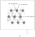
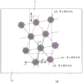
Fig. 1 is a layout view of conductive particles P in an anisotropic conductive film 1A according to an embodiment of the present invention. The anisotropic conductive film 1A includes an insulating adhesive layer 10 and conductive particles P fixed to the insulating adhesive layer 10 in a lattice-like arrangement.
In the anisotropic conductive film 1A, the conductive particles P are arbitrarily contained in the film0And the conductive particles P0When the shortest distance between adjacent conductive particles is set as the 1 st center-to-center distance d1 and the second shortest distance is set as the 2 nd center-to-center distance d2, the distance between the adjacent conductive particles and the conductive particle P is set to be equal to the distance between the adjacent conductive particles and the center of the conductive particle P0Conductive particles P spaced apart by a 1 st center spacing d11And conductive particles P0Conductive particles P spaced apart by 2 nd center spacing2Forming an acute triangle P0P1P2The conductive particles pass through the conductive particles P0、P1Is arranged at a pitch d1 in the 1 st arrangement direction L1, and conductive particles are also arranged along the passing conductive particles P1、P2Is aligned in the 2 nd alignment direction L2, the conductive particles are aligned along the direction passing through the conductive particles P0、P2Is arranged at a pitch d2 in the 3 rd arrangement direction L3. Further, in the present embodiment, the pitch d2 of the conductive particles in the 3 rd arrangement direction is larger than the pitch d1 of the conductive particles in the 1 st arrangement direction L1, but these pitches may be the same.
The particle diameter D of the conductive particles P is preferably 1 to 10 μm from the viewpoint of the prevention of short circuit and the stability of bonding between electrodes.
The 1 st center-to-center distance D1 and the 2 nd center-to-center distance D2 are each 1.5 to 5 times, preferably 1.8 to 4.5 times, and more preferably 2 to 4 times the particle diameter D of the conductive particles. If the 1 st center-to-center pitch d1 and the 2 nd center-to-center pitch d2 are too short, short circuits are likely to occur when terminals are connected using an anisotropic conductive film, and conversely, if they are too long, the number of conductive particles trapped between the terminals is insufficient.
The difference between the 1 st center-to-center distance D1 and the 2 nd center-to-center distance D2 is preferably less than 2 times, more preferably less than 1.5 times, and even more preferably equal or less than the particle diameter D of the conductive particles P. If this difference is too large, the capturing ability of the bump at the time of anisotropic conductive connection using the anisotropic conductive film 1A is deteriorated.
The density of the conductive particles P is preferably 2000 to 250000/mm2. The particle density is appropriately adjusted according to the particle diameter and arrangement direction of the conductive particles P.
Even when an anisotropic conductive film in which conductive particles are arranged in a lattice shape at a predetermined density is manufactured, the conductive particles may fall off from the lattice position in an actual manufacturing method. Regarding the phenomenon that the conductive particles fall off from the lattice positions, in the anisotropic conductive film 1A, the number of continuous conductive particles P falling off is preferably 6 or less, more preferably 5 or less, and further preferably 4 or less with respect to each of the 1 st alignment direction L1 and the 2 nd alignment direction L2, particularly, each of the alignment directions L1, L2, and L3. In addition, when 10 regions are continuously drawn in the 1 st arrangement direction and 10 regions are continuously drawn in the 2 nd arrangement direction from the arrangement position of any conductive particle, that is, 10 × 10 (total 100) arrangement positions are drawn, in 100 arrangement positions, 75 or more conductive particles are preferably present, more preferably 80 or more, further preferably 90 or more, and particularly preferably 94 or more.
By suppressing the falling-off of the conductive particles in this way, when the square bumps are connected by using the anisotropic conductive film, the conductive particles can be easily captured in an amount sufficient for conduction in the bumps regardless of the portion of the anisotropic conductive film, and the connection can be made with anisotropic conductivity at a fine pitch.
As a method for suppressing the falling-off of the conductive particles in this way, it is preferable to repeatedly perform wiping on a die or a member having through holes when the conductive particles P are disposed on the insulating adhesive layer 10 as described later.
In addition, in the anisotropic conductive film 1A, the inclination angle alpha of the 2 nd arrangement direction is 18-35 degrees. By determining the inclination angle α in the 2 nd alignment direction in the relationship between the particle diameter D and the pitches D1 and D2, a sufficient number of conductive particles contributing to conduction can be secured regardless of where the rectangular region used for the anisotropic conductive connection is located in the film surface of the anisotropic conductive film 1A when the rectangular connection terminals (bumps) are anisotropically connected through the anisotropic conductive film 1A.
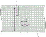
In general, regarding anisotropic conductive connection in a production line of electronic equipment, the width direction of the connection terminal 3 is generally arranged along the longitudinal direction of the anisotropic conductive film 1A. Therefore, from the viewpoint of productivity of the anisotropic conductive film, as shown in fig. 2, it is preferable to make the longitudinal direction Lt of the rectangular connection terminal 3 coincide with the direction L0 orthogonal to the 1 st arrangement direction L1 (i.e., to make the width direction of the connection terminal 3 coincide with the 1 st arrangement direction L1). In other words, it is desirable that the 1 st alignment direction L1 be formed substantially parallel to the longitudinal direction Lf of the anisotropic conductive film 1A, that is, the 1 st alignment direction L1 of the conductive particles be formed parallel to the longitudinal direction Lf of the anisotropic conductive film 1A within a range of variation in the arrangement of the conductive particles that occurs when the anisotropic conductive film is manufactured.
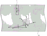
On the other hand, from the viewpoint of improving the trapping property of the conductive particles in the connection terminal at the time of anisotropic conductive connection, it is preferable that any one of the 1 st alignment direction L1, the 2 nd alignment direction L2, and the 3 rd alignment direction L3 of the conductive particles P is inclined with respect to the longitudinal direction of the anisotropic conductive film 1B as in the anisotropic conductive film 1B shown in fig. 3. In particular, an acute angle β (hereinafter, also referred to as an inclination angle β) formed between the 1 st alignment direction L1 and the longitudinal direction Lf of the anisotropic conductive film 1B is preferably 5 to 25 °.
The anisotropic conductive film 1B is configured in the same manner as the anisotropic conductive film 1A described above, except that the 1 st alignment direction L1 of the conductive particles P is inclined with respect to the longitudinal direction Lf of the anisotropic conductive film 1B.
Here, since the conductive particles are arranged in a close state so that the anisotropic conductive film can be connected to terminals with a finer pitch, as shown in fig. 4 described later, an outer tangent line (two-dot chain line) of the conductive particle P in a direction perpendicular to the longitudinal direction Lf of the anisotropic conductive film 1B may penetrate the conductive particles Pc and Pe adjacent to the conductive particle P. This makes it possible to further increase the area occupied by the conductive particles on the connection surface of the connection terminal 3 in a plan view in which the anisotropic conductive film 1B is superimposed on the terminal surface of the connection terminal 3. Therefore, the number of conductive particles P that are sandwiched between the opposing connection terminals 3 and are pressed into the connection terminals 3 to conduct between the connection terminals 3 during anisotropic conductive connection can be prevented from being insufficient.
As long as the anisotropic conductive film of the present invention is configured with the conductive particles as described above, various modes can be adopted for the configuration of the conductive particles P themselves, the layer configuration of the insulating adhesive layer 10, or the constituent resin.
That is, the conductive particles P can be appropriately selected from conductive particles used in well-known anisotropic conductive films and used. Examples thereof include metal particles such as nickel, cobalt, silver, copper, gold, and palladium, and metal-coated resin particles. More than 2 kinds can be used simultaneously.
As the insulating adhesive layer 10, an insulating resin layer used for a known anisotropic conductive film can be suitably used. For example, a photoradical polymerization type resin layer containing an acrylate compound and a photoradical polymerization initiator, a thermal radical polymerization type resin layer containing an acrylate compound and a thermal radical polymerization initiator, a thermal cationic polymerization type resin layer containing an epoxy compound and a thermal cationic polymerization initiator, a thermal anionic polymerization type resin layer containing an epoxy compound and a thermal anionic polymerization initiator, and the like can be used. Further, these resin layers can be polymerized separately as necessary. Further, the insulating adhesive layer 10 may be formed of a plurality of resin layers.
Further, an insulating filler such as silica fine particles, alumina, or aluminum hydroxide may be added to the insulating adhesive layer 10 as necessary. Preferably, the amount of the insulating filler is 3 to 40 parts by mass per 100 parts by mass of the resin forming the insulating adhesive layer. Thus, even if the insulating adhesive layer 10 melts during anisotropic conductive connection, wasteful movement of the conductive particles 2 due to the melted resin can be suppressed.
As a method for fixing the conductive particles P to the insulating adhesive layer 10 by the above arrangement, a mold having recesses corresponding to the arrangement of the conductive particles P is prepared by a known method such as machining, laser processing, photolithography, or the like, the conductive particles are put into the mold, the insulating adhesive layer forming composition is filled in the conductive particles, the composition is cured, and the conductive particles are taken out from the mold. The mold may be made of a material having lower rigidity than such a mold.
In order to provide the conductive particles P in the above-described arrangement on the insulating adhesive layer 10, the following method or the like may be used: the insulating adhesive layer-forming composition layer is provided with a member having through holes formed in a predetermined arrangement, and the conductive particles P are supplied from the member and passed through the through holes.
When anisotropic conductive films 1A and 1B of the present invention are used to anisotropically conductively connect a connection terminal of a 1 st electronic component such as a flexible substrate or a glass substrate and a connection terminal of a 2 nd electronic component such as an IC chip or an IC module, as shown in fig. 2 and 3, a longitudinal direction Lf of each of anisotropic conductive films 1A and 1B is aligned with a width direction of a connection terminal 3 of the 1 st electronic component or the 2 nd electronic component. Accordingly, the arrangement of the conductive particles P in the anisotropic conductive films 1A and 1B of the present invention can be effectively utilized to sufficiently increase the number of the conductive particles P captured in the connection terminal, and particularly, in the case of using the anisotropic conductive film 1B in which the alignment direction of the conductive particles P is inclined with respect to the longitudinal direction Lf of the anisotropic conductive film, the capturing property of the conductive particles P in the connection terminal 3 can be significantly improved.
For example, when COG connection of high-density wiring is performed using a glass substrate or the like on which a connection terminal is formed through a transparent electrode as a 1 st electronic component and an IC chip or the like as a 2 nd electronic component, more specifically, when the size of the connection surface of these connection terminals is 8 to 60 μm in width and 400 μm or less in length (the lower limit is equal to the width), or when the width of the connection surface of the connection terminal in the width direction is less than 7 times the particle diameter of the conductive particles, the number of conductive particles that can be captured by the connection terminal is stably increased compared to conventional anisotropic conductive connection, and connection reliability can be improved. Further, if the width of the connection terminal surface in the width direction is smaller than the above case, connection failure often occurs, and if it is larger than the above case, it is difficult to cope with high-density mounting required for COG connection. Further, if the length of the connection terminal surface is shorter than the above case, it is difficult to obtain stable conduction, and if the length is longer than the above case, it becomes a factor of partial contact. On the other hand, the minimum distance between the connection terminals is determined in accordance with the width of the connection surface of the connection terminals in the width direction, and can be, for example, 8 to 30 μm.
In addition, in the fine pitch terminals that can be connected by the anisotropic conductive film of the present invention, the minimum terminal pitch (the distance may be shifted in the parallel direction within the range in which anisotropic connection is possible) in which the terminals including the opposing terminals connected to each other are adjacent to each other with a gap in the parallel direction can be made smaller than 4 times the conductive particle diameter. In this case, the width of the connection surface of the connected terminal in the width direction can be less than 7 times the particle diameter of the conductive particles.
The present invention also includes a connection structure of the 1 st electronic component and the 2 nd electronic component which are anisotropically conductively connected in this manner.
Examples
The present invention will be specifically described below based on examples.
Experimental example 1
Regarding the arrangement of the conductive particles P (particle diameter D is 4 μm) in the anisotropic conductive film, when the 1 st center pitch D1 is 10 μm and the 2 nd center pitch D2 is 10 μm and the inclination angle α is changed as shown in table 1, the maximum number of particles and the minimum number of particles of the conductive particles that can be captured by the bump before heating and pressing are determined by superimposing a narrow bump having an electrode size of 15 μm × 100 μm on the pattern of the anisotropic conductive film. In this case, the longitudinal direction of the anisotropic conductive film is aligned with the width direction of the bump. Particles falling off at 50% or more of the area with respect to the edge portion of the bump are not counted as conductive particles that can be captured by the bump.
From the results, the inclination angle α and the particle capturing property of the bump were observed. The results are shown in table 1.
[ Table 1]
| Angle of inclination alpha (°) | 0° | 5° | 15° | 18° | 20° | 25° | 30° | 35° | 40° | 45° |
| Maximum number of particles | 20 are provided with | 13 are provided with | 13 are provided with | 14 are provided with | 14 are provided with | 14 are provided with | 18 are provided with | 18 are provided with | 13 are provided with | 14 are provided with |
| Minimum number of |
9 are provided with | 9 are provided with | 9 are provided with | 11 are provided with | 11 are provided with | 12 pieces of | 12 pieces of | 12 pieces of | 7 are provided with | 7 are provided with |
As can be seen from table 1, when the inclination angle α is 18 to 35 °, the difference between the minimum number and the maximum number of the numbers of particles captured by the bump is small and stable, and the method is effective for a narrow bump.
On the other hand, if the inclination angle α is too small, the difference in the number of captures becomes large. This is because the progress of the particle alignment at the end of the bump is directly affected by the capture number due to the excessively small tilt angle. Even if the inclination angle α is excessively large, the same phenomenon occurs, and particles falling off from the bumps tend to increase.
As described above, it is known that in the case of a narrow bump, when the capture efficiency is constant in order to stably maintain the conductivity, the inclination angle α needs to be appropriately maintained.
Examples 1 to 8, comparative examples 1 to 5
Next, in order to specifically examine the relationship between the inter-particle distance of the conductive particles and the tilt angle α, an anisotropic conductive film in which the conductive particles (AUL 704, particle size 4 μm) were arranged as shown in table 2 was produced as follows, using the resins shown in table 2. That is, a mixed solution of an insulating resin containing a thermoplastic resin, a thermosetting resin and a latent curing agent was prepared in the composition shown in table 2, and the mixed solution was applied to a PET film having a film thickness of 50 μm, and the mixed solution was dried in an oven at 80 ℃ for 5 minutes to form an adhesive layer having a thickness of 20 μm on the PET film.
On the other hand, the resin molds having the array patterns of the convex portions were prepared in the arrangement shown in table 2, and the well-known transparent resin pellets were poured into the metal molds in a molten state and cooled and solidified, whereby the concave portions formed the resin molds having the array patterns shown in table 2. The concave portion of the resin mold is filled with conductive particles, the adhesive layer of the insulating resin is coated on the concave portion, and the thermosetting resin contained in the insulating resin is cured by ultraviolet curing. Then, the insulating resin was peeled off from the mold, and the anisotropic conductive films of examples and comparative examples were produced.
Examples 9 to 13, comparative examples 6 and 7
Anisotropic conductive films of examples 9 to 13 and comparative examples 6 and 7 were produced in the same manner as in the above examples and comparative examples, except that the conductive particles were arranged as shown in table 3.
Here, comparative example 7 had a tetragonal lattice shape, and examples 3, 9 to 13 had a hexagonal lattice shape.
In comparative examples 1 and 6, the conductive particles were dispersed in a low boiling point solvent to form a spray, and were randomly arranged on the same plane.
The center-to-center distance d (1 st center-to-center distance d1 and 2 nd center-to-center distance d 2) between adjacent conductive particles was measured and confirmed using an optical microscope. In this case, 100 50 groups in the 1 st alignment direction or the 2 nd alignment direction were arbitrarily measured, and the average value thereof was obtained to confirm that the distance d between adjacent particle centers was expected. The results are shown in table 2.
On the other hand, in comparative examples 1 and 6, 100 conductive particles were arbitrarily selected, and the center-to-center distance between the nearest conductive particles was measured.
Evaluation of
The anisotropic conductive films of the examples and comparative examples were evaluated for (a) the number of particles captured, (b) the initial on-resistance, (c) the on-reliability, and (d) the occurrence of short circuits, as follows. The results are shown in tables 2 and 3.
(a) Number of particle traps
(a-1) average number
Using the anisotropic conductive films of examples and comparative examples, 100 bumps of 15X 100 μm were heated and pressed (180 ℃ C., 80MPa, 5 seconds) against a glass substrate to obtain a connection. In this case, the longitudinal direction of the anisotropic conductive film is aligned with the width direction of the bump. Then, the number of particles captured in each bump was measured, and the average number of particles captured per 1 bump was determined.
(a-2) minimum number
The minimum number of the number of particles captured by each bump measured in (a-1) is determined.
(b) Initial on-resistance
The anisotropic conductive films of the examples and comparative examples were sandwiched between the IC for evaluation of initial conduction and conduction reliability and a glass substrate, and heated and pressed (180 ℃, 80MPa, 5 seconds) to obtain each of the connections for evaluation. In this case, the longitudinal direction of the anisotropic conductive film is aligned with the width direction of the bump. Then, the on-resistance of the evaluation connector was measured.
Here, the dimensions of the evaluation ICs and the glass substrate corresponding to the terminal patterns are as follows.
IC for evaluating initial conduction and conduction reliability
Outer diameter of 0.7X 20mm
Thickness of 0.2mm
Bump specification gold plating, height 12 μm, size 15X 100 μm, bump pitch 15 μm
Glass substrate
Manufactured by glass Corning Corp Ltd
Outer diameter of 30X 50mm
Thickness of 0.5mm
Electrode ITO wiring
(c) Conduction reliability
The on-resistance of the anisotropic conductive film evaluation connectors obtained in the examples and comparative examples and the IC for evaluation obtained in (b) was measured in the same manner as in (b) after being left in a constant temperature bath at 85 ℃ and 85% RH for 500 hours. Further, if the on-resistance is 5 Ω or more, it is not preferable from the viewpoint of the on-stability of the electronic component to be connected in actual use.
(d) Incidence of short circuits
As an IC for evaluation of the short-circuit occurrence rate, a second IC (comb element group (TEG)) having 7.5 μm-spaced comb teeth was prepared.
External diameter of 1.5X 13mm
Thickness of 0.5mm
Bump specification gold plating, height of 15 μm, size of 25X 140 μm, bump pitch of 7.5 μm
The anisotropic conductive films of the examples and comparative examples were sandwiched between an evaluation IC for short-circuit occurrence rate and a glass substrate having a pattern corresponding to the evaluation IC. Heating and pressurizing under the same connection conditions as in (b) to obtain a connected product, and determining the short circuit occurrence rate of the connected product. The short-circuit occurrence rate was calculated as "the number of short-circuits occurred/the total number of 7.5 μm intervals". If the short-circuit occurrence rate is 1ppm or more, it is not preferable from the viewpoint of producing a practically used connection structure.

(note) × 1: xinri iron-gold YP-50 (thermoplastic resin)
*2: mitsubishi chemical, jER828 (thermosetting resin)
*3: sanxin chemical industry, SI-60L (latent hardener)

(note) × 1: xinri iron-gold YP-50 (thermoplastic resin)
*2: mitsubishi chemical, jER828 (thermosetting resin)
*3: sanxin chemical industry, SI-60L (latent hardener)
As is clear from table 2, if the inclination angle α of the conductive particles is 18 to 35 °, the initial on resistance is low, the on reliability is high, the occurrence rate of short circuit is suppressed, and anisotropic conductive connection corresponding to high-density wiring having a terminal width of about 4 times the particle diameter is possible.
On the other hand, it is found that in comparative example 1, the insulation property is poor due to the excessively high particle density, and in comparative examples 2 to 5, the number of particles captured in the bump is small and the conduction reliability is insufficient because the inclination angle α deviates from the range of 18 to 35 °.
Further, as is clear from table 3, examples 9 to 13 in which the respective alignment directions of the conductive particles are inclined in the longitudinal direction of the anisotropic conductive film are also excellent in conduction reliability and reduced in the occurrence rate of short circuit. However, when a connection object for evaluation in which an IC for evaluation of initial conduction and conduction reliability was connected to a glass substrate using the anisotropic conductive films of examples 9 to 13 was observed, as in the arrangement of conductive particles shown in fig. 4, an outer tangent line (dashed-two dotted line) of the conductive particle P in the longitudinal direction Lt of the bump 3 overlapped with the conductive particles Pc and Pe adjacent to the conductive particle P, and the outer tangent line penetrated through the conductive particles Pc and Pe. This confirmed that even if the width of the bump 3 was further narrowed, a sufficient number of conductive particles could be captured to obtain conduction.
In addition, if the appearances of the evaluation connectors using the anisotropic conductive films of comparative example 7 and examples 9 to 13 are compared, in the evaluation connectors using the anisotropic conductive films of examples 9 to 13, the difference in the indentation state between the conductive particles Pc located at the center in the width direction of the bump 3 and the conductive particles Pe located at the edge of the bump 3 is smaller than that of the evaluation connector using the anisotropic conductive film of comparative example 7. From this, it was found that if the anisotropic conductive film of the example is used, more uniform pressure bonding can be achieved. Further, since the bump area is small, it is not necessary to capture conductive particles at both the edge and the center in the width direction in one bump 3, and the above-described result is obtained by observing conductive particles captured at the edge and conductive particles captured at the center in the width direction in any of a plurality of bumps connected in parallel.
Examples 14 to 19
In examples 3 and 9 to 13, the particle diameter D of the conductive particles was changed from 4 μm to 3 μm, the center distance between adjacent particles was set to 6 μm (that is, (D-D)/D was 1), and the arrangement density was 28000 pieces/mm2The anisotropic conductive films of examples 14 to 19 were produced and evaluated in the same manner. As a result, the following effects substantially similar to those of examples 3 and 9 to 13 were obtained also in these examples: the initial on-resistance is low, the on-reliability is high, and the occurrence rate of short circuit is restrained. The indentation states of the conductive particles located at the edges of the bumps and the conductive particles located at the center in the width direction in these evaluation connectors were also the same as in examples 9 to 13.
The number density of the particles prepared in example 14 and comparative example 1 was 60000 particles/mm2The anisotropic conductive film of (2) is used with a bump area of 700 μm2Bump IC having bump size of 14 μm × 50 μm and bump pitch of 14 μm, and its implementationThe measurement of the number of captured particles in example 1 was performed in the same manner, and the frequency of the conductive particles captured by the 1 bump was examined. The results are shown in fig. 5.
As is clear from fig. 5, in example 14, the number of captured conductive particles per 1 bump was about 9 on average, and the frequency of appearance was rapidly increased, as compared with comparative example 1, and the number of captured conductive particles per 1 bump was stable on average.
Examples 20 to 25
In examples 3 and 9 to 13, conductive particles were produced with a particle size D of 4 μm, a center distance between adjacent particles of 7 μm ((D-D)/D: 0.75), and an arrangement density of 20000 particles/mm2) The anisotropic conductive films of examples 20 to 25 were evaluated in the same manner as described above. As a result, the following effects substantially similar to those of examples 3, 9 to 13 were obtained also in these examples: the initial on-resistance is low, the on-reliability is high, and the occurrence rate of short circuit is restrained. The indentation states of the conductive particles located at the edges of the bumps and the conductive particles located at the center in the width direction in these evaluation connectors were also the same as in examples 9 to 13.
Examples 26 to 31
In examples 3 and 9 to 13, conductive particles were produced with a particle size D of 4 μm and a center distance between adjacent particles of 16 μm ((D-D)/D: 3), and the arrangement density was 4000 particles/mm2) The anisotropic conductive films of examples 26 to 31 were evaluated in the same manner. As a result, although the initial on-resistance was higher in these examples than in examples 3, 9 to 13, there was no problem in practical use. The effects of high conduction reliability and suppression of the occurrence of short circuits are the same as in examples 3 and 9 to 13. This is considered because the anisotropic conductive films of examples 26 to 31 have a low arrangement density of conductive particles. The indentation states of the conductive particles located at the edge of the bump in the evaluation connection and the conductive particles located at the center in the width direction were the same as in examples 9 to 13.
Examples 32 to 33
In examples 5 and 7, 20 parts by mass of a silica fine particle filler (silica fine particles, アエロジル RY200 (AEROSIL RY 200), japan アエロジル corporation, japan) was added to 100 parts by mass of an insulating resin, and anisotropic conductive films were produced and evaluated in the same manner as in examples 5 and 7. As a result, the following effects similar to those of examples 5 and 7 were obtained: the initial on-resistance is low, the on-reliability is high, and the occurrence rate of short circuit is restrained.
Description of the reference symbols
1A, 1B Anisotropic conductive film
3 connecting terminal or bump
10 insulating adhesive layer
L0 is orthogonal to the 1 st arrangement direction
L2 alignment direction 2
Length direction of Lf anisotropic conductive film
Length direction of Lt connection terminal
d1 center to center spacing
d2 center to center spacing
Particle diameter of D conductive particles
P、P0、P1、P2Pc, Pe conductive particles
Angle of inclination alpha
Beta tilt angle.
Claims (24)
1. An anisotropic conductive film comprising an insulating adhesive layer and conductive particles arranged in a lattice form on the insulating adhesive layer, wherein,
in the case where the shortest distance to an arbitrary conductive particle is set as the 1 st center-to-center distance and the second shortest distance is set as the 2 nd center-to-center distance with respect to the center-to-center distance between the arbitrary conductive particle and the conductive particle adjacent to the arbitrary conductive particle,
the 1 st center-to-center distance and the 2 nd center-to-center distance are each 1.5 to 5 times the particle diameter of the conductive particles,
with respect to the composition of the random conductive particles P0And optionally conductive particles P0Conductive particles P spaced apart by 1 st center spacing1And with optional conductive particles P0Conductive particles P spaced apart from 1 st-center spacing or 2 nd-center spacing2Forming an acute triangle with respect to the passing conductive particle P0、P1And a straight line orthogonal to the direction of the straight line and the passing conductive particle P1、P2An acute angle alpha formed by the directions of the straight lines is 18 to 35 DEG, wherein the conductive particles P pass through0、P1Is the 1 st alignment direction, passing through the conductive particles P1、P2Is referred to as the 2 nd alignment direction,
will pass through the conductive particles P0、P2Is set to the 3 rd arrangement direction, the 1 st arrangement direction, the 2 nd arrangement direction and the 3 rd arrangement direction are inclined with respect to the longitudinal direction of the anisotropic conductive film,
the angle formed by the 1 st alignment direction and the film longitudinal direction is smaller than the angle formed by the 2 nd alignment direction and the film longitudinal direction.
2. The anisotropic conductive film of claim 1, wherein a difference between the 1 st center-to-center distance and the 2 nd center-to-center distance is less than 2 times a particle diameter of the conductive particles.
3. The anisotropic conductive film according to claim 1, wherein an angle β formed by the 1 st alignment direction and the longitudinal direction of the anisotropic conductive film is 5 to 25 °.
4. The anisotropic conductive film according to claim 1, wherein the density of the conductive particles is 2000 to 250000 particles/mm2。
5. The anisotropic conductive film according to claim 1, wherein the number of continuous drops of the conductive particles in each of the 1 st alignment direction and the 2 nd alignment direction is 6 or less.
6. The anisotropic conductive film according to any of claims 1 to 5, wherein the insulating adhesive layer is composed of a plurality of resin layers.
7. A connecting method for anisotropically conductively connecting a connecting terminal of a 1 st electronic component and a connecting terminal of a 2 nd electronic component using the anisotropically conductive film according to any one of claims 1 to 6, wherein a longitudinal direction of the anisotropically conductive film is made to coincide with a width direction of the connecting terminal of the 1 st electronic component or the 2 nd electronic component, and a direction substantially orthogonal to a 1 st alignment direction of the anisotropically conductive film is made to coincide with a longitudinal direction of the connecting terminal of the 1 st electronic component or the 2 nd electronic component.
8. The connecting method according to claim 7, wherein the 1 st electronic component is a glass substrate on which a connecting terminal is formed through a transparent electrode, and the 2 nd electronic component is an IC chip.
9. The connecting method according to claim 7 or 8, wherein the size of the connecting surface of the connecting terminal is 8 to 60 μm in width and 400 μm or less in length.
10. A connection structure wherein the connection terminal of the 1 st electronic component and the connection terminal of the 2 nd electronic component are anisotropically conductively connected through the anisotropic conductive film according to any one of claims 1 to 6,
wherein the length direction of the anisotropic conductive film is aligned with the width direction of the connection terminal of the 1 st electronic component or the 2 nd electronic component.
11. A method for manufacturing a connection structure, wherein a connection structure is manufactured, the connection structure being formed by connecting a connection terminal of a 1 st electronic component and a connection terminal of a 2 nd electronic component through the anisotropic conductive film according to any one of claims 1 to 6,
wherein the length direction of the anisotropic conductive film is aligned with the width direction of the connection terminal of the 1 st electronic component or the 2 nd electronic component.
12. An anisotropic conductive film used for anisotropic conductive connection between a connection terminal of a 1 st electronic component and a connection terminal of a 2 nd electronic component, comprising an insulating adhesive layer and conductive particles arranged in a lattice form in the insulating adhesive layer,
in the case where the shortest distance to an arbitrary conductive particle is set as the 1 st center-to-center distance and the second shortest distance is set as the 2 nd center-to-center distance with respect to the center-to-center distance between the arbitrary conductive particle and the conductive particle adjacent to the arbitrary conductive particle,
the 1 st center-to-center distance and the 2 nd center-to-center distance are each 1.5 to 5 times the particle diameter of the conductive particles,
with respect to the composition of the random conductive particles P0And optionally conductive particles P0Conductive particles P spaced apart by 1 st center spacing1And with optional conductive particles P0Conductive particles P spaced apart from 1 st-center spacing or 2 nd-center spacing2Forming an acute triangle with respect to the passing conductive particle P0、P1And a straight line orthogonal to the direction of the straight line and the passing conductive particle P1、P2An acute angle alpha formed by the directions of the straight lines is 18 to 35 DEG, wherein the conductive particles P pass through0、P1Is the 1 st alignment direction, passing through the conductive particles P1、P2Is referred to as the 2 nd alignment direction,
will pass through the conductive particles P0、P2Is set to the 3 rd arrangement direction, the 1 st arrangement direction, the 2 nd arrangement direction and the 3 rd arrangement direction are inclined with respect to the longitudinal direction of the anisotropic conductive film,
the angle beta formed by the 1 st alignment direction and the length direction of the anisotropic conductive film is 5 to 25 degrees.
13. The anisotropic conductive film of claim 12, wherein a difference between the 1 st center-to-center distance and the 2 nd center-to-center distance is less than 2 times a particle diameter of the conductive particles.
14. The anisotropic conductive film according to claim 12, wherein the density of the conductive particles is 2000 to 250000 particles/mm2。
15. The anisotropic conductive film according to claim 12, wherein the number of continuous drops of the conductive particles in each of the 1 st alignment direction and the 2 nd alignment direction is 6 or less.
16. The anisotropic conductive film according to any of claims 12 to 15, wherein the insulating adhesive layer is composed of a plurality of resin layers.
17. A connection structure wherein the connection terminal of the 1 st electronic component and the connection terminal of the 2 nd electronic component are anisotropically conductively connected through the anisotropic conductive film according to any one of claims 12 to 16,
wherein the length direction of the anisotropic conductive film is aligned with the width direction of the connection terminal of the 1 st electronic component or the 2 nd electronic component.
18. A method for manufacturing a connection structure, wherein a connection structure is manufactured, the connection structure being formed by connecting a connection terminal of a 1 st electronic component and a connection terminal of a 2 nd electronic component through the anisotropic conductive film according to any one of claims 12 to 16,
wherein the length direction of the anisotropic conductive film is aligned with the width direction of the connection terminal of the 1 st electronic component or the 2 nd electronic component.
19. An anisotropic conductive film comprising an insulating adhesive layer and conductive particles arranged in a lattice form on the insulating adhesive layer, wherein,
in the case where the shortest distance to an arbitrary conductive particle is set as the 1 st center-to-center distance and the second shortest distance is set as the 2 nd center-to-center distance with respect to the center-to-center distance between the arbitrary conductive particle and the conductive particle adjacent to the arbitrary conductive particle,
the 1 st center-to-center distance and the 2 nd center-to-center distance are each 1.5 to 5 times the particle diameter of the conductive particles,
with respect to the composition of the random conductive particles P0And optionally conductive particles P0Conductive particles P spaced apart by 1 st center spacing1And with optional conductive particles P0Conductive particles P spaced apart from 1 st-center spacing or 2 nd-center spacing2Forming an acute triangle with respect to the passing conductive particle P0、P1And a straight line orthogonal to the direction of the straight line and the passing conductive particle P1、P2An acute angle alpha formed by the directions of the straight lines is 18 to 35 DEG, wherein the conductive particles P pass through0、P1Is the 1 st alignment direction, passing through the conductive particles P1、P2Is referred to as the 2 nd alignment direction,
the conductive particles P adjacent to the conductive particles P are penetrated by an outer tangent line of the conductive particles P in a direction orthogonal to the longitudinal direction of the anisotropic conductive film.
20. A connecting method of anisotropically conductively connecting a connecting terminal of a 1 st electronic component and a connecting terminal of a 2 nd electronic component using the anisotropically conductive film according to claim 19, wherein a longitudinal direction of the anisotropically conductive film is made to coincide with a width direction of the connecting terminal of the 1 st electronic component or the 2 nd electronic component, and a direction substantially orthogonal to a 1 st arrangement direction of the anisotropically conductive film is made to coincide with a longitudinal direction of the connecting terminal of the 1 st electronic component or the 2 nd electronic component.
21. The connecting method according to claim 20, wherein the 1 st electronic component is a glass substrate on which a connecting terminal is formed through a transparent electrode, and the 2 nd electronic component is an IC chip.
22. The connecting method according to claim 20 or 21, wherein the size of the connecting surface of the connecting terminal is 8 to 60 μm in width and 400 μm or less in length.
23. A connection structure wherein the connection terminal of the 1 st electronic component and the connection terminal of the 2 nd electronic component are anisotropically conductively connected through the anisotropically conductive film according to claim 19,
wherein the length direction of the anisotropic conductive film is aligned with the width direction of the connection terminal of the 1 st electronic component or the 2 nd electronic component.
24. A method for producing a connection structure wherein a connection structure is produced in which a connection terminal of a 1 st electronic component and a connection terminal of a 2 nd electronic component are anisotropically conductively connected through the anisotropic conductive film according to claim 19,
wherein the length direction of the anisotropic conductive film is aligned with the width direction of the connection terminal of the 1 st electronic component or the 2 nd electronic component.
Applications Claiming Priority (7)
| Application Number | Priority Date | Filing Date | Title |
|---|---|---|---|
| JP2013239180 | 2013-11-19 | ||
| JP2013-239180 | 2013-11-19 | ||
| JP2014-193168 | 2014-09-22 | ||
| JP2014193168 | 2014-09-22 | ||
| JP2014-219793 | 2014-10-28 | ||
| JP2014219793A JP6119718B2 (en) | 2013-11-19 | 2014-10-28 | Anisotropic conductive film and connection structure |
| CN201480057445.1A CN105637712B (en) | 2013-11-19 | 2014-11-18 | Anisotropic conductive film and connecting structure body |
Related Parent Applications (1)
| Application Number | Title | Priority Date | Filing Date |
|---|---|---|---|
| CN201480057445.1A Division CN105637712B (en) | 2013-11-19 | 2014-11-18 | Anisotropic conductive film and connecting structure body |
Publications (2)
| Publication Number | Publication Date |
|---|---|
| CN108539440A CN108539440A (en) | 2018-09-14 |
| CN108539440B true CN108539440B (en) | 2020-12-01 |
Family
ID=55804233
Family Applications (3)
| Application Number | Title | Priority Date | Filing Date |
|---|---|---|---|
| CN201710112148.8A Pending CN107123471A (en) | 2013-11-19 | 2014-11-18 | Anisotropic conductive film and connecting structure body |
| CN201810229524.6A Active CN108539440B (en) | 2013-11-19 | 2014-11-18 | Anisotropic conductive film and connection structure |
| CN201480057445.1A Active CN105637712B (en) | 2013-11-19 | 2014-11-18 | Anisotropic conductive film and connecting structure body |
Family Applications Before (1)
| Application Number | Title | Priority Date | Filing Date |
|---|---|---|---|
| CN201710112148.8A Pending CN107123471A (en) | 2013-11-19 | 2014-11-18 | Anisotropic conductive film and connecting structure body |
Family Applications After (1)
| Application Number | Title | Priority Date | Filing Date |
|---|---|---|---|
| CN201480057445.1A Active CN105637712B (en) | 2013-11-19 | 2014-11-18 | Anisotropic conductive film and connecting structure body |
Country Status (6)
| Country | Link |
|---|---|
| US (3) | US10522502B2 (en) |
| JP (6) | JP6119718B2 (en) |
| KR (4) | KR20200029640A (en) |
| CN (3) | CN107123471A (en) |
| HK (1) | HK1257883A1 (en) |
| TW (2) | TWI699054B (en) |
Families Citing this family (24)
| Publication number | Priority date | Publication date | Assignee | Title |
|---|---|---|---|---|
| JP6119718B2 (en) * | 2013-11-19 | 2017-04-26 | デクセリアルズ株式会社 | Anisotropic conductive film and connection structure |
| KR20240025047A (en) | 2013-11-19 | 2024-02-26 | 데쿠세리아루즈 가부시키가이샤 | Anisotropic electroconductive film and connection structure |
| JP7052254B2 (en) | 2016-11-04 | 2022-04-12 | デクセリアルズ株式会社 | Filler-containing film |
| SG10201909698RA (en) * | 2015-01-13 | 2019-11-28 | Dexerials Corp | Anisotropic conductive film |
| JP7095227B2 (en) * | 2016-05-05 | 2022-07-05 | デクセリアルズ株式会社 | Anisotropic conductive film |
| WO2017191781A1 (en) * | 2016-05-05 | 2017-11-09 | デクセリアルズ株式会社 | Anisotropic electroconductive film |
| WO2017191772A1 (en) * | 2016-05-05 | 2017-11-09 | デクセリアルズ株式会社 | Filler alignment film |
| JP7274811B2 (en) | 2016-05-05 | 2023-05-17 | デクセリアルズ株式会社 | anisotropic conductive film |
| WO2017191779A1 (en) * | 2016-05-05 | 2017-11-09 | デクセリアルズ株式会社 | Anisotropic conductive film |
| WO2017191774A1 (en) * | 2016-05-05 | 2017-11-09 | デクセリアルズ株式会社 | Anisotropic conductive film |
| JP7274810B2 (en) | 2016-05-05 | 2023-05-17 | デクセリアルズ株式会社 | anisotropic conductive film |
| US20170338204A1 (en) * | 2016-05-17 | 2017-11-23 | Taiwan Semiconductor Manufacturing Company, Ltd. | Device and Method for UBM/RDL Routing |
| CN115691861A (en) * | 2016-12-01 | 2023-02-03 | 迪睿合株式会社 | Connection structure |
| JP7047282B2 (en) | 2016-12-01 | 2022-04-05 | デクセリアルズ株式会社 | Filler-containing film |
| CN116253914A (en) | 2016-12-01 | 2023-06-13 | 迪睿合株式会社 | Filler-containing film |
| KR102002694B1 (en) * | 2017-09-29 | 2019-07-23 | 주식회사 새한마이크로텍 | Conductive contact and anisotropic conductive sheet with the same |
| KR102519126B1 (en) * | 2018-03-30 | 2023-04-06 | 삼성디스플레이 주식회사 | Display device |
| TW202019022A (en) | 2018-06-06 | 2020-05-16 | 日商迪睿合股份有限公司 | Connector, method for manufacturing connector, and connection method |
| JP7330768B2 (en) | 2018-06-06 | 2023-08-22 | デクセリアルズ株式会社 | Method for manufacturing and connection of connecting body |
| WO2020032150A1 (en) * | 2018-08-08 | 2020-02-13 | デクセリアルズ株式会社 | Anisotropic electroconductive film |
| CN112534650B (en) * | 2018-08-08 | 2023-05-23 | 迪睿合株式会社 | Anisotropic conductive film |
| JP2020095922A (en) * | 2018-12-14 | 2020-06-18 | デクセリアルズ株式会社 | Anisotropic conductive film |
| JP6794591B1 (en) * | 2019-05-20 | 2020-12-02 | タツタ電線株式会社 | Conductive adhesive sheet |
| US20230369531A1 (en) | 2021-03-26 | 2023-11-16 | Dexerials Corporation | Method of manufacturing display device |
Citations (2)
| Publication number | Priority date | Publication date | Assignee | Title |
|---|---|---|---|---|
| WO1997045893A1 (en) * | 1996-05-31 | 1997-12-04 | The Whitaker Corporation | Anisotropic conductive film |
| EP2075836A1 (en) * | 2007-12-27 | 2009-07-01 | FUJIFILM Corporation | Microstructure and method of manufacturing the same |
Family Cites Families (34)
| Publication number | Priority date | Publication date | Assignee | Title |
|---|---|---|---|---|
| BE794600A (en) | 1972-01-28 | 1973-05-16 | Usel Hubert | CARTRIDGE WITHOUT CASE FOR ELECTRIC FIRE |
| JP3472987B2 (en) * | 1993-01-29 | 2003-12-02 | 日立化成工業株式会社 | Manufacturing method of connecting member and manufacturing apparatus therefor |
| JP3624818B2 (en) | 1999-10-12 | 2005-03-02 | ソニーケミカル株式会社 | Anisotropic conductive connection material, connection body, and manufacturing method thereof |
| JP2001307555A (en) | 2000-04-17 | 2001-11-02 | Sony Corp | Anisotropic conductive film, its assembly method, and circuit board using the same |
| JP4190763B2 (en) * | 2001-04-27 | 2008-12-03 | 旭化成株式会社 | Conductive adhesive sheet having anisotropy and method for producing the same |
| JP3886401B2 (en) | 2002-03-25 | 2007-02-28 | ソニーケミカル&インフォメーションデバイス株式会社 | Method for manufacturing connection structure |
| JP4130747B2 (en) * | 2002-03-28 | 2008-08-06 | 旭化成エレクトロニクス株式会社 | Anisotropic conductive adhesive sheet and manufacturing method thereof |
| JP2008274300A (en) * | 2003-01-07 | 2008-11-13 | Sekisui Chem Co Ltd | Curable resin composition |
| JP3849680B2 (en) * | 2003-10-06 | 2006-11-22 | セイコーエプソン株式会社 | Substrate bonded body manufacturing method, substrate bonded body, electro-optical device manufacturing method, and electro-optical device |
| JP4907840B2 (en) * | 2003-11-12 | 2012-04-04 | 日立化成工業株式会社 | Anisotropic conductive film and circuit board using the same |
| JP2006233203A (en) | 2005-01-31 | 2006-09-07 | Asahi Kasei Electronics Co Ltd | Anisotropically electroconductive adhesive film |
| JP2007009176A (en) * | 2005-01-31 | 2007-01-18 | Asahi Kasei Electronics Co Ltd | Anisotropically electroconductive adhesive film |
| JP4887700B2 (en) * | 2005-09-09 | 2012-02-29 | 住友ベークライト株式会社 | Anisotropic conductive film and electronic / electrical equipment |
| KR100961417B1 (en) * | 2005-09-29 | 2010-06-09 | 아사히 가세이 케미칼즈 가부시키가이샤 | High-stability microencapsulated hardener for epoxy resin and epoxy resin composition |
| CN101849322B (en) | 2007-09-20 | 2012-07-04 | 索尼化学&信息部件株式会社 | Anisotropic conductive film and its production method, and bonded body employing anisotropic conductive film |
| CN101835859B (en) * | 2007-10-29 | 2015-04-08 | 日立化成株式会社 | Circuit connecting material, connection structure and method for producing the same |
| JP2009135388A (en) | 2007-10-30 | 2009-06-18 | Hitachi Chem Co Ltd | Circuit connecting method |
| WO2010001900A1 (en) | 2008-07-01 | 2010-01-07 | 日立化成工業株式会社 | Circuit connection material and circuit connection structure |
| JP5540559B2 (en) * | 2009-05-11 | 2014-07-02 | デクセリアルズ株式会社 | Method for producing film adhesive for circuit connection |
| JP5375374B2 (en) | 2009-07-02 | 2013-12-25 | 日立化成株式会社 | Circuit connection material and circuit connection structure |
| JP5516016B2 (en) | 2010-04-23 | 2014-06-11 | デクセリアルズ株式会社 | Anisotropic conductive adhesive film and manufacturing method thereof |
| JP5614135B2 (en) * | 2010-07-06 | 2014-10-29 | デクセリアルズ株式会社 | Anisotropic conductive adhesive, manufacturing method thereof, connection structure and manufacturing method thereof |
| KR101242235B1 (en) * | 2010-07-28 | 2013-03-11 | 세키스이가가쿠 고교가부시키가이샤 | Insulating-particle-adhered electrically conductive particle, process for producing insulating-particle-adhered electrically conductive particle, anisotropic conductive material, and connected structure |
| JP5318840B2 (en) * | 2010-11-08 | 2013-10-16 | デクセリアルズ株式会社 | Anisotropic conductive film, method for manufacturing anisotropic conductive film, connection method between electronic members, and connection structure |
| JP5643623B2 (en) * | 2010-12-02 | 2014-12-17 | デクセリアルズ株式会社 | Anisotropic conductive material and method for producing the same |
| CN102176337B (en) * | 2011-01-06 | 2013-01-09 | 天津大学 | Composite conductive particles for anisotropic conductive film and preparation method |
| JP2011102404A (en) * | 2011-02-17 | 2011-05-26 | Sony Chemical & Information Device Corp | Anisotropic conductive film |
| JP2011181525A (en) | 2011-06-09 | 2011-09-15 | Sony Chemical & Information Device Corp | Anisotropic conductive material |
| WO2013024544A1 (en) | 2011-08-18 | 2013-02-21 | 日立化成工業株式会社 | Adhesive material reel |
| JP2013077557A (en) | 2011-09-13 | 2013-04-25 | Sekisui Chem Co Ltd | Anisotropic conductive material and connection structure |
| CN103258585A (en) * | 2012-02-17 | 2013-08-21 | 鸿富锦精密工业(深圳)有限公司 | Anisotropic conductive film and manufacturing device and manufacturing method thereof |
| JP2014219793A (en) * | 2013-05-07 | 2014-11-20 | コニカミノルタ株式会社 | Handwriting input correction program, handwriting input correction method and handwriting input device |
| CN105359342B (en) * | 2013-07-31 | 2018-02-23 | 迪睿合株式会社 | Anisotropic conductive film and its manufacture method |
| JP6119718B2 (en) * | 2013-11-19 | 2017-04-26 | デクセリアルズ株式会社 | Anisotropic conductive film and connection structure |
-
2014
- 2014-10-28 JP JP2014219793A patent/JP6119718B2/en active Active
- 2014-11-18 KR KR1020207007393A patent/KR20200029640A/en not_active IP Right Cessation
- 2014-11-18 US US15/030,509 patent/US10522502B2/en active Active
- 2014-11-18 CN CN201710112148.8A patent/CN107123471A/en active Pending
- 2014-11-18 KR KR1020197012986A patent/KR20190052161A/en active Application Filing
- 2014-11-18 KR KR1020167010177A patent/KR20160088294A/en active Search and Examination
- 2014-11-18 KR KR1020187010853A patent/KR20180041777A/en not_active Application Discontinuation
- 2014-11-18 CN CN201810229524.6A patent/CN108539440B/en active Active
- 2014-11-18 CN CN201480057445.1A patent/CN105637712B/en active Active
- 2014-11-19 TW TW107138270A patent/TWI699054B/en active
- 2014-11-19 TW TW107110076A patent/TWI643417B/en active
-
2017
- 2017-03-28 JP JP2017063281A patent/JP6640141B2/en active Active
- 2017-03-28 JP JP2017063298A patent/JP6380591B2/en active Active
-
2018
- 2018-06-08 US US16/003,310 patent/US10510711B2/en active Active
- 2018-07-17 JP JP2018134336A patent/JP6932110B2/en active Active
-
2019
- 2019-01-08 HK HK19100244.3A patent/HK1257883A1/en unknown
- 2019-09-23 US US16/578,763 patent/US11139265B2/en active Active
-
2020
- 2020-04-27 JP JP2020078370A patent/JP2020129550A/en active Pending
-
2022
- 2022-06-17 JP JP2022098047A patent/JP2022133317A/en active Pending
Patent Citations (2)
| Publication number | Priority date | Publication date | Assignee | Title |
|---|---|---|---|---|
| WO1997045893A1 (en) * | 1996-05-31 | 1997-12-04 | The Whitaker Corporation | Anisotropic conductive film |
| EP2075836A1 (en) * | 2007-12-27 | 2009-07-01 | FUJIFILM Corporation | Microstructure and method of manufacturing the same |
Also Published As
| Publication number | Publication date |
|---|---|
| JP6119718B2 (en) | 2017-04-26 |
| JP6380591B2 (en) | 2018-08-29 |
| CN108539440A (en) | 2018-09-14 |
| TWI643417B (en) | 2018-12-01 |
| KR20160088294A (en) | 2016-07-25 |
| JP2022133317A (en) | 2022-09-13 |
| US20200020664A1 (en) | 2020-01-16 |
| JP6932110B2 (en) | 2021-09-08 |
| US10522502B2 (en) | 2019-12-31 |
| JP2017139233A (en) | 2017-08-10 |
| JP2019009129A (en) | 2019-01-17 |
| KR20180041777A (en) | 2018-04-24 |
| CN105637712A (en) | 2016-06-01 |
| TW201826624A (en) | 2018-07-16 |
| KR20200029640A (en) | 2020-03-18 |
| JP2017188446A (en) | 2017-10-12 |
| JP6640141B2 (en) | 2020-02-05 |
| US20180294246A1 (en) | 2018-10-11 |
| JP2016066573A (en) | 2016-04-28 |
| US10510711B2 (en) | 2019-12-17 |
| KR20190052161A (en) | 2019-05-15 |
| CN107123471A (en) | 2017-09-01 |
| TWI699054B (en) | 2020-07-11 |
| JP2020129550A (en) | 2020-08-27 |
| US20160270225A1 (en) | 2016-09-15 |
| US11139265B2 (en) | 2021-10-05 |
| HK1257883A1 (en) | 2019-11-01 |
| CN105637712B (en) | 2019-08-20 |
| TW201909485A (en) | 2019-03-01 |
Similar Documents
| Publication | Publication Date | Title |
|---|---|---|
| CN108539440B (en) | Anisotropic conductive film and connection structure | |
| CN110499119B (en) | Anisotropic conductive film and connection structure | |
| JP7176550B2 (en) | Anisotropic conductive film and connection structure | |
| JP6690184B2 (en) | Anisotropically conductive film and connection structure | |
| TWI675088B (en) | Anisotropic conductive film and connection structure | |
| KR102639862B1 (en) | Connection body and connection body production method | |
| TWI834084B (en) | Anisotropic conductive film and its manufacturing method, and a connection structure using an anisotropic conductive film and its manufacturing method |
Legal Events
| Date | Code | Title | Description |
|---|---|---|---|
| PB01 | Publication | ||
| PB01 | Publication | ||
| SE01 | Entry into force of request for substantive examination | ||
| SE01 | Entry into force of request for substantive examination | ||
| REG | Reference to a national code |
Ref country code: HK Ref legal event code: DE Ref document number: 1257883 Country of ref document: HK |
|
| GR01 | Patent grant | ||
| GR01 | Patent grant |