CN108429552B - Analog-to-digital converter and semiconductor device using the same - Google Patents
Analog-to-digital converter and semiconductor device using the same Download PDFInfo
- Publication number
- CN108429552B CN108429552B CN201711129593.1A CN201711129593A CN108429552B CN 108429552 B CN108429552 B CN 108429552B CN 201711129593 A CN201711129593 A CN 201711129593A CN 108429552 B CN108429552 B CN 108429552B
- Authority
- CN
- China
- Prior art keywords
- code
- hysteresis circuits
- circuits
- register array
- hysteresis
- Prior art date
- Legal status (The legal status is an assumption and is not a legal conclusion. Google has not performed a legal analysis and makes no representation as to the accuracy of the status listed.)
- Active
Links
- 239000004065 semiconductor Substances 0.000 title claims description 22
- 230000003213 activating effect Effects 0.000 claims description 7
- 238000006243 chemical reaction Methods 0.000 claims description 7
- 238000010586 diagram Methods 0.000 description 5
- 238000003491 array Methods 0.000 description 2
- 239000003990 capacitor Substances 0.000 description 2
- 238000000034 method Methods 0.000 description 2
- 230000000630 rising effect Effects 0.000 description 2
- 238000007792 addition Methods 0.000 description 1
- 238000012217 deletion Methods 0.000 description 1
- 230000037430 deletion Effects 0.000 description 1
- 238000004519 manufacturing process Methods 0.000 description 1
- 238000012986 modification Methods 0.000 description 1
- 230000004048 modification Effects 0.000 description 1
Images


Classifications
-
- H—ELECTRICITY
- H03—ELECTRONIC CIRCUITRY
- H03M—CODING; DECODING; CODE CONVERSION IN GENERAL
- H03M1/00—Analogue/digital conversion; Digital/analogue conversion
- H03M1/12—Analogue/digital converters
- H03M1/18—Automatic control for modifying the range of signals the converter can handle, e.g. gain ranging
- H03M1/181—Automatic control for modifying the range of signals the converter can handle, e.g. gain ranging in feedback mode, i.e. by determining the range to be selected from one or more previous digital output values
- H03M1/182—Automatic control for modifying the range of signals the converter can handle, e.g. gain ranging in feedback mode, i.e. by determining the range to be selected from one or more previous digital output values the feedback signal controlling the reference levels of the analogue/digital converter
-
- H—ELECTRICITY
- H03—ELECTRONIC CIRCUITRY
- H03M—CODING; DECODING; CODE CONVERSION IN GENERAL
- H03M1/00—Analogue/digital conversion; Digital/analogue conversion
- H03M1/12—Analogue/digital converters
- H03M1/124—Sampling or signal conditioning arrangements specially adapted for A/D converters
- H03M1/129—Means for adapting the input signal to the range the converter can handle, e.g. limiting, pre-scaling ; Out-of-range indication
- H03M1/1295—Clamping, i.e. adjusting the DC level of the input signal to a predetermined value
-
- H—ELECTRICITY
- H03—ELECTRONIC CIRCUITRY
- H03M—CODING; DECODING; CODE CONVERSION IN GENERAL
- H03M1/00—Analogue/digital conversion; Digital/analogue conversion
- H03M1/12—Analogue/digital converters
- H03M1/18—Automatic control for modifying the range of signals the converter can handle, e.g. gain ranging
-
- H—ELECTRICITY
- H03—ELECTRONIC CIRCUITRY
- H03K—PULSE TECHNIQUE
- H03K5/00—Manipulating of pulses not covered by one of the other main groups of this subclass
- H03K5/22—Circuits having more than one input and one output for comparing pulses or pulse trains with each other according to input signal characteristics, e.g. slope, integral
- H03K5/24—Circuits having more than one input and one output for comparing pulses or pulse trains with each other according to input signal characteristics, e.g. slope, integral the characteristic being amplitude
- H03K5/2472—Circuits having more than one input and one output for comparing pulses or pulse trains with each other according to input signal characteristics, e.g. slope, integral the characteristic being amplitude using field effect transistors
- H03K5/2481—Circuits having more than one input and one output for comparing pulses or pulse trains with each other according to input signal characteristics, e.g. slope, integral the characteristic being amplitude using field effect transistors with at least one differential stage
-
- H—ELECTRICITY
- H03—ELECTRONIC CIRCUITRY
- H03K—PULSE TECHNIQUE
- H03K5/00—Manipulating of pulses not covered by one of the other main groups of this subclass
- H03K5/22—Circuits having more than one input and one output for comparing pulses or pulse trains with each other according to input signal characteristics, e.g. slope, integral
- H03K5/24—Circuits having more than one input and one output for comparing pulses or pulse trains with each other according to input signal characteristics, e.g. slope, integral the characteristic being amplitude
- H03K5/2472—Circuits having more than one input and one output for comparing pulses or pulse trains with each other according to input signal characteristics, e.g. slope, integral the characteristic being amplitude using field effect transistors
- H03K5/249—Circuits having more than one input and one output for comparing pulses or pulse trains with each other according to input signal characteristics, e.g. slope, integral the characteristic being amplitude using field effect transistors using clock signals
-
- H—ELECTRICITY
- H03—ELECTRONIC CIRCUITRY
- H03M—CODING; DECODING; CODE CONVERSION IN GENERAL
- H03M1/00—Analogue/digital conversion; Digital/analogue conversion
- H03M1/002—Provisions or arrangements for saving power, e.g. by allowing a sleep mode, using lower supply voltage for downstream stages, using multiple clock domains or by selectively turning on stages when needed
-
- H—ELECTRICITY
- H03—ELECTRONIC CIRCUITRY
- H03M—CODING; DECODING; CODE CONVERSION IN GENERAL
- H03M1/00—Analogue/digital conversion; Digital/analogue conversion
- H03M1/06—Continuously compensating for, or preventing, undesired influence of physical parameters
- H03M1/0602—Continuously compensating for, or preventing, undesired influence of physical parameters of deviations from the desired transfer characteristic
- H03M1/0604—Continuously compensating for, or preventing, undesired influence of physical parameters of deviations from the desired transfer characteristic at one point, i.e. by adjusting a single reference value, e.g. bias or gain error
- H03M1/0607—Offset or drift compensation
-
- H—ELECTRICITY
- H03—ELECTRONIC CIRCUITRY
- H03M—CODING; DECODING; CODE CONVERSION IN GENERAL
- H03M1/00—Analogue/digital conversion; Digital/analogue conversion
- H03M1/06—Continuously compensating for, or preventing, undesired influence of physical parameters
- H03M1/0617—Continuously compensating for, or preventing, undesired influence of physical parameters characterised by the use of methods or means not specific to a particular type of detrimental influence
- H03M1/0675—Continuously compensating for, or preventing, undesired influence of physical parameters characterised by the use of methods or means not specific to a particular type of detrimental influence using redundancy
- H03M1/0678—Continuously compensating for, or preventing, undesired influence of physical parameters characterised by the use of methods or means not specific to a particular type of detrimental influence using redundancy using additional components or elements, e.g. dummy components
-
- H—ELECTRICITY
- H03—ELECTRONIC CIRCUITRY
- H03M—CODING; DECODING; CODE CONVERSION IN GENERAL
- H03M1/00—Analogue/digital conversion; Digital/analogue conversion
- H03M1/10—Calibration or testing
- H03M1/1009—Calibration
- H03M1/1014—Calibration at one point of the transfer characteristic, i.e. by adjusting a single reference value, e.g. bias or gain error
- H03M1/1019—Calibration at one point of the transfer characteristic, i.e. by adjusting a single reference value, e.g. bias or gain error by storing a corrected or correction value in a digital look-up table
-
- H—ELECTRICITY
- H03—ELECTRONIC CIRCUITRY
- H03M—CODING; DECODING; CODE CONVERSION IN GENERAL
- H03M1/00—Analogue/digital conversion; Digital/analogue conversion
- H03M1/12—Analogue/digital converters
- H03M1/14—Conversion in steps with each step involving the same or a different conversion means and delivering more than one bit
-
- H—ELECTRICITY
- H03—ELECTRONIC CIRCUITRY
- H03M—CODING; DECODING; CODE CONVERSION IN GENERAL
- H03M1/00—Analogue/digital conversion; Digital/analogue conversion
- H03M1/12—Analogue/digital converters
- H03M1/34—Analogue value compared with reference values
- H03M1/38—Analogue value compared with reference values sequentially only, e.g. successive approximation type
- H03M1/46—Analogue value compared with reference values sequentially only, e.g. successive approximation type with digital/analogue converter for supplying reference values to converter
- H03M1/462—Details of the control circuitry, e.g. of the successive approximation register
-
- H—ELECTRICITY
- H03—ELECTRONIC CIRCUITRY
- H03M—CODING; DECODING; CODE CONVERSION IN GENERAL
- H03M1/00—Analogue/digital conversion; Digital/analogue conversion
- H03M1/12—Analogue/digital converters
- H03M1/50—Analogue/digital converters with intermediate conversion to time interval
- H03M1/56—Input signal compared with linear ramp
-
- H—ELECTRICITY
- H03—ELECTRONIC CIRCUITRY
- H03M—CODING; DECODING; CODE CONVERSION IN GENERAL
- H03M1/00—Analogue/digital conversion; Digital/analogue conversion
- H03M1/66—Digital/analogue converters
- H03M1/72—Sequential conversion in series-connected stages
-
- H—ELECTRICITY
- H04—ELECTRIC COMMUNICATION TECHNIQUE
- H04N—PICTORIAL COMMUNICATION, e.g. TELEVISION
- H04N25/00—Circuitry of solid-state image sensors [SSIS]; Control thereof
- H04N25/70—SSIS architectures; Circuits associated therewith
- H04N25/76—Addressed sensors, e.g. MOS or CMOS sensors
- H04N25/767—Horizontal readout lines, multiplexers or registers
-
- H—ELECTRICITY
- H03—ELECTRONIC CIRCUITRY
- H03M—CODING; DECODING; CODE CONVERSION IN GENERAL
- H03M1/00—Analogue/digital conversion; Digital/analogue conversion
-
- H—ELECTRICITY
- H03—ELECTRONIC CIRCUITRY
- H03M—CODING; DECODING; CODE CONVERSION IN GENERAL
- H03M1/00—Analogue/digital conversion; Digital/analogue conversion
- H03M1/12—Analogue/digital converters
-
- H—ELECTRICITY
- H03—ELECTRONIC CIRCUITRY
- H03M—CODING; DECODING; CODE CONVERSION IN GENERAL
- H03M1/00—Analogue/digital conversion; Digital/analogue conversion
- H03M1/66—Digital/analogue converters
- H03M1/74—Simultaneous conversion
- H03M1/80—Simultaneous conversion using weighted impedances
- H03M1/802—Simultaneous conversion using weighted impedances using capacitors, e.g. neuron-mos transistors, charge coupled devices
- H03M1/804—Simultaneous conversion using weighted impedances using capacitors, e.g. neuron-mos transistors, charge coupled devices with charge redistribution
Landscapes
- Engineering & Computer Science (AREA)
- Theoretical Computer Science (AREA)
- Physics & Mathematics (AREA)
- Nonlinear Science (AREA)
- Multimedia (AREA)
- Signal Processing (AREA)
- Analogue/Digital Conversion (AREA)
Abstract
一种模数转换器包括:第一DAC单元,其被配置为根据第一码来改变通过第一节点输出的参考电压的电平;第二DAC单元,其基于第一节点而并联耦接到第一DAC单元,并且被配置为根据第二码来改变参考电压的电平;比较器,其被配置为通过将输入电压与参考电压进行比较来产生比较结果信号;以及至少一个寄存器阵列,其被配置为储存具有初始值的第一码和第二码,并且通过根据比较结果信号改变第一码和第二码的值来储存第一码和第二码。
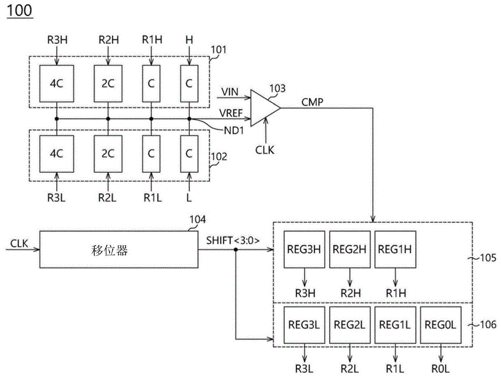
An analog-to-digital converter includes: a first DAC unit configured to change a level of a reference voltage output through a first node according to a first code; and a second DAC unit coupled in parallel based on the first node a first DAC unit configured to change the level of the reference voltage according to the second code; a comparator configured to generate a comparison result signal by comparing the input voltage with the reference voltage; and at least one register array which is configured to store the first code and the second code having initial values, and store the first code and the second code by changing the values of the first code and the second code according to the comparison result signal.
Description
Claims (20)
Applications Claiming Priority (2)
| Application Number | Priority Date | Filing Date | Title |
|---|---|---|---|
| KR10-2017-0019541 | 2017-02-13 | ||
| KR1020170019541A KR102654276B1 (en) | 2017-02-13 | 2017-02-13 | Analog to digital converter and semiconductor apparatus using the same |
Publications (2)
| Publication Number | Publication Date |
|---|---|
| CN108429552A CN108429552A (en) | 2018-08-21 |
| CN108429552B true CN108429552B (en) | 2021-12-31 |
Family
ID=60788882
Family Applications (1)
| Application Number | Title | Priority Date | Filing Date |
|---|---|---|---|
| CN201711129593.1A Active CN108429552B (en) | 2017-02-13 | 2017-11-15 | Analog-to-digital converter and semiconductor device using the same |
Country Status (4)
| Country | Link |
|---|---|
| US (1) | US9859910B1 (en) |
| KR (2) | KR102654276B1 (en) |
| CN (1) | CN108429552B (en) |
| TW (1) | TWI734847B (en) |
Families Citing this family (4)
| Publication number | Priority date | Publication date | Assignee | Title |
|---|---|---|---|---|
| US10334196B2 (en) * | 2016-01-25 | 2019-06-25 | Semiconductor Energy Laboratory Co., Ltd. | Semiconductor device |
| WO2018235403A1 (en) * | 2017-06-23 | 2018-12-27 | 日立オートモティブシステムズ株式会社 | Electronic control device |
| CN114300015B (en) * | 2021-12-30 | 2024-09-20 | 厦门半导体工业技术研发有限公司 | In-memory data processing circuit and resistive random access memory |
| CN115865081B (en) * | 2022-11-30 | 2024-10-01 | 贵州振华风光半导体股份有限公司 | Error reduction circuit, method and comparator array |
Family Cites Families (12)
| Publication number | Priority date | Publication date | Assignee | Title |
|---|---|---|---|---|
| JP2011188240A (en) * | 2010-03-09 | 2011-09-22 | Panasonic Corp | Successive approximation type ad converter, and mobile radio device |
| JP5427663B2 (en) * | 2010-03-24 | 2014-02-26 | スパンション エルエルシー | A / D converter |
| CN102480297B (en) * | 2010-11-29 | 2014-05-14 | 苏州华芯微电子股份有限公司 | Successive comparison type AD converter |
| US8416105B2 (en) * | 2011-02-17 | 2013-04-09 | Taiwan Semiconductor Manufacturing Company, Ltd. | ADC calibration apparatus |
| CN102355266B (en) * | 2011-07-28 | 2016-03-02 | 上海华虹宏力半导体制造有限公司 | A kind of successive approximation register analog-digital converter |
| US8638248B2 (en) * | 2011-10-07 | 2014-01-28 | Nxp, B.V. | Input-independent self-calibration method and apparatus for successive approximation analog-to-digital converter with charge-redistribution digital to analog converter |
| US8981973B2 (en) | 2013-03-08 | 2015-03-17 | Microchip Technology Incorporated | Successive-approximation-register (SAR) analog-to-digital converter (ADC) attenuation capacitor calibration method and apparatus |
| KR102103933B1 (en) * | 2013-09-04 | 2020-04-24 | 삼성전자주식회사 | Successive approximation analog to digital converter and method of analog to digital conversion |
| CN104660261B (en) * | 2013-11-19 | 2019-01-29 | 山东共达电声股份有限公司 | A kind of analog-digital commutator of adaptive quantizing |
| CN104124972B (en) * | 2014-08-08 | 2017-05-10 | 西安电子科技大学 | 10-bit ultra-low-power successive approximation register analog-to-digital converter based on charge redistribution |
| WO2016061784A1 (en) * | 2014-10-23 | 2016-04-28 | Lattice Semiconductor Corporation | Successive approximation register-based analog-to-digital converter with increased time frame for digital-to-analog capacitor settling |
| US9432037B2 (en) * | 2014-11-05 | 2016-08-30 | Samsung Electronics Co., Ltd | Apparatus and method for analog-digital converting |
-
2017
- 2017-02-13 KR KR1020170019541A patent/KR102654276B1/en active Active
- 2017-06-26 US US15/632,648 patent/US9859910B1/en active Active
- 2017-10-13 TW TW106135000A patent/TWI734847B/en active
- 2017-11-15 CN CN201711129593.1A patent/CN108429552B/en active Active
-
2023
- 2023-10-17 KR KR1020230138891A patent/KR102685478B1/en active Active
Also Published As
| Publication number | Publication date |
|---|---|
| KR102685478B1 (en) | 2024-07-17 |
| KR20230148310A (en) | 2023-10-24 |
| US9859910B1 (en) | 2018-01-02 |
| KR102654276B1 (en) | 2024-04-04 |
| KR20180093445A (en) | 2018-08-22 |
| TW201830872A (en) | 2018-08-16 |
| CN108429552A (en) | 2018-08-21 |
| TWI734847B (en) | 2021-08-01 |
Similar Documents
| Publication | Publication Date | Title |
|---|---|---|
| KR102001762B1 (en) | DAC capacitance array, SAR-type analog-to-digital converter and method of reducing power consumption | |
| US8081097B2 (en) | Analog-to-digital converter and related calibrating comparator | |
| KR102685478B1 (en) | Analog to digital converter and semiconductor apparatus using the same | |
| US9998131B1 (en) | Hybrid analog-to-digital converter | |
| CN107493104A (en) | Successive approximation register analog-to-digital converter and analog-to-digital signal conversion method thereof | |
| CN110752847A (en) | digital to analog converter | |
| US9374088B2 (en) | Impedance calibration apparatus of semiconductor integrated circuit | |
| CN113014264A (en) | Analog-digital converter with multi-mode selection | |
| JP2019097121A (en) | Latched comparator | |
| CN110034762B (en) | Sampling frequency adjustable analog-digital converter | |
| US7429945B2 (en) | Analog to digital converter | |
| US12184302B2 (en) | Data register unit, SAR ADC and electronic device | |
| US6747588B1 (en) | Method for improving successive approximation analog-to-digital converter | |
| US10305452B2 (en) | Five-level switched-capacitance DAC using bootstrapped switches | |
| JP2010124405A (en) | Analog/digital conversion circuit | |
| CN117957780B (en) | Multi-stage analog-to-digital converter for crossbar switching circuit | |
| CN214675121U (en) | A multi-mode selection analog-to-digital converter | |
| CN115882862A (en) | Resistor-Based Digital-to-Analog Converters | |
| TWI477082B (en) | Successive approximation analog to digital converter with a direct switching technique for capacitor array through comparator output and method thereof | |
| US12273119B2 (en) | Analog-to-digital converter circuit and semiconductor integrated circuit | |
| JP2014138371A (en) | Successive approximation ad converter and method of operating the same | |
| CN120811386A (en) | Analog-to-digital conversion circuit based on small-value priority and double-end differential capacitor | |
| JP2005229257A (en) | Analog / digital converter and microcomputer equipped with the same | |
| CN114301462A (en) | Successive approximation type analog-to-digital converter and switch control method | |
| CN117478144A (en) | Capacitor Weighted Segmented Buffer |
Legal Events
| Date | Code | Title | Description |
|---|---|---|---|
| PB01 | Publication | ||
| PB01 | Publication | ||
| SE01 | Entry into force of request for substantive examination | ||
| SE01 | Entry into force of request for substantive examination | ||
| GR01 | Patent grant | ||
| GR01 | Patent grant | ||
| TR01 | Transfer of patent right | ||
| TR01 | Transfer of patent right |
Effective date of registration: 20240613 Address after: American Texas Patentee after: Mimi IP Co.,Ltd. Country or region after: U.S.A. Address before: Gyeonggi Do, South Korea Patentee before: Sk Hynix Inc. Country or region before: Republic of Korea |