CN107533298B - Mask forming method and method for manufacturing printed wiring board using the same - Google Patents
Mask forming method and method for manufacturing printed wiring board using the same Download PDFInfo
- Publication number
- CN107533298B CN107533298B CN201680023007.2A CN201680023007A CN107533298B CN 107533298 B CN107533298 B CN 107533298B CN 201680023007 A CN201680023007 A CN 201680023007A CN 107533298 B CN107533298 B CN 107533298B
- Authority
- CN
- China
- Prior art keywords
- layer
- base material
- mask
- resin
- material layer
- Prior art date
- Legal status (The legal status is an assumption and is not a legal conclusion. Google has not performed a legal analysis and makes no representation as to the accuracy of the status listed.)
- Active
Links
- 238000000034 method Methods 0.000 title claims abstract description 107
- 238000004519 manufacturing process Methods 0.000 title claims abstract description 47
- 239000000463 material Substances 0.000 claims abstract description 135
- 239000007864 aqueous solution Substances 0.000 claims abstract description 124
- 239000011347 resin Substances 0.000 claims abstract description 108
- 229920005989 resin Polymers 0.000 claims abstract description 108
- 230000002378 acidificating effect Effects 0.000 claims abstract description 93
- 238000007650 screen-printing Methods 0.000 claims abstract description 21
- 230000001678 irradiating effect Effects 0.000 claims abstract description 13
- 229910052751 metal Inorganic materials 0.000 claims description 92
- 239000002184 metal Substances 0.000 claims description 92
- 229910045601 alloy Inorganic materials 0.000 claims description 53
- 239000000956 alloy Substances 0.000 claims description 53
- 239000000758 substrate Substances 0.000 claims description 48
- 239000003795 chemical substances by application Substances 0.000 claims description 44
- QAOWNCQODCNURD-UHFFFAOYSA-N Sulfuric acid Chemical compound OS(O)(=O)=O QAOWNCQODCNURD-UHFFFAOYSA-N 0.000 claims description 40
- VEXZGXHMUGYJMC-UHFFFAOYSA-N Hydrochloric acid Chemical compound Cl VEXZGXHMUGYJMC-UHFFFAOYSA-N 0.000 claims description 38
- -1 polyoxyethylene Polymers 0.000 claims description 28
- XLYOFNOQVPJJNP-UHFFFAOYSA-N water Substances O XLYOFNOQVPJJNP-UHFFFAOYSA-N 0.000 claims description 25
- PXHVJJICTQNCMI-UHFFFAOYSA-N Nickel Chemical compound [Ni] PXHVJJICTQNCMI-UHFFFAOYSA-N 0.000 claims description 23
- 239000010949 copper Substances 0.000 claims description 23
- 239000004020 conductor Substances 0.000 claims description 21
- 229910052802 copper Inorganic materials 0.000 claims description 21
- 229920003171 Poly (ethylene oxide) Polymers 0.000 claims description 20
- 239000002253 acid Substances 0.000 claims description 20
- RYGMFSIKBFXOCR-UHFFFAOYSA-N Copper Chemical compound [Cu] RYGMFSIKBFXOCR-UHFFFAOYSA-N 0.000 claims description 19
- XEEYBQQBJWHFJM-UHFFFAOYSA-N Iron Chemical compound [Fe] XEEYBQQBJWHFJM-UHFFFAOYSA-N 0.000 claims description 19
- 238000001035 drying Methods 0.000 claims description 18
- 238000010438 heat treatment Methods 0.000 claims description 13
- 229910052759 nickel Inorganic materials 0.000 claims description 13
- USIUVYZYUHIAEV-UHFFFAOYSA-N diphenyl ether Chemical class C=1C=CC=CC=1OC1=CC=CC=C1 USIUVYZYUHIAEV-UHFFFAOYSA-N 0.000 claims description 12
- BASFCYQUMIYNBI-UHFFFAOYSA-N platinum Chemical compound [Pt] BASFCYQUMIYNBI-UHFFFAOYSA-N 0.000 claims description 12
- 229910052782 aluminium Inorganic materials 0.000 claims description 11
- 239000000243 solution Substances 0.000 claims description 11
- XAGFODPZIPBFFR-UHFFFAOYSA-N aluminium Chemical compound [Al] XAGFODPZIPBFFR-UHFFFAOYSA-N 0.000 claims description 10
- 229910052718 tin Inorganic materials 0.000 claims description 10
- ATJFFYVFTNAWJD-UHFFFAOYSA-N Tin Chemical compound [Sn] ATJFFYVFTNAWJD-UHFFFAOYSA-N 0.000 claims description 9
- RTAQQCXQSZGOHL-UHFFFAOYSA-N Titanium Chemical compound [Ti] RTAQQCXQSZGOHL-UHFFFAOYSA-N 0.000 claims description 9
- PCHJSUWPFVWCPO-UHFFFAOYSA-N gold Chemical compound [Au] PCHJSUWPFVWCPO-UHFFFAOYSA-N 0.000 claims description 9
- 229910052737 gold Inorganic materials 0.000 claims description 9
- 239000010931 gold Substances 0.000 claims description 9
- 229910052742 iron Inorganic materials 0.000 claims description 9
- 238000007747 plating Methods 0.000 claims description 9
- 229910052709 silver Inorganic materials 0.000 claims description 9
- 239000004332 silver Substances 0.000 claims description 9
- 229910052719 titanium Inorganic materials 0.000 claims description 9
- 239000010936 titanium Substances 0.000 claims description 9
- 239000004693 Polybenzimidazole Substances 0.000 claims description 8
- FEWJPZIEWOKRBE-UHFFFAOYSA-N Tartaric acid Natural products [H+].[H+].[O-]C(=O)C(O)C(O)C([O-])=O FEWJPZIEWOKRBE-UHFFFAOYSA-N 0.000 claims description 8
- 229910017052 cobalt Inorganic materials 0.000 claims description 8
- 239000010941 cobalt Substances 0.000 claims description 8
- GUTLYIVDDKVIGB-UHFFFAOYSA-N cobalt atom Chemical compound [Co] GUTLYIVDDKVIGB-UHFFFAOYSA-N 0.000 claims description 8
- 238000005323 electroforming Methods 0.000 claims description 8
- 229920002480 polybenzimidazole Polymers 0.000 claims description 8
- 239000011975 tartaric acid Substances 0.000 claims description 8
- 235000002906 tartaric acid Nutrition 0.000 claims description 8
- HEMHJVSKTPXQMS-UHFFFAOYSA-M Sodium hydroxide Chemical compound [OH-].[Na+] HEMHJVSKTPXQMS-UHFFFAOYSA-M 0.000 claims description 6
- 239000003822 epoxy resin Substances 0.000 claims description 6
- 239000011521 glass Substances 0.000 claims description 6
- 229910052697 platinum Inorganic materials 0.000 claims description 6
- 229920000647 polyepoxide Polymers 0.000 claims description 6
- WQGWDDDVZFFDIG-UHFFFAOYSA-N pyrogallol Chemical compound OC1=CC=CC(O)=C1O WQGWDDDVZFFDIG-UHFFFAOYSA-N 0.000 claims description 6
- BQCADISMDOOEFD-UHFFFAOYSA-N Silver Chemical compound [Ag] BQCADISMDOOEFD-UHFFFAOYSA-N 0.000 claims description 5
- 239000000919 ceramic Substances 0.000 claims description 5
- 238000010030 laminating Methods 0.000 claims description 5
- 229920000728 polyester Polymers 0.000 claims description 5
- 229920001721 polyimide Polymers 0.000 claims description 5
- CDBYLPFSWZWCQE-UHFFFAOYSA-L Sodium Carbonate Chemical compound [Na+].[Na+].[O-]C([O-])=O CDBYLPFSWZWCQE-UHFFFAOYSA-L 0.000 claims description 4
- 230000007935 neutral effect Effects 0.000 claims description 4
- 239000009719 polyimide resin Substances 0.000 claims description 4
- 239000010453 quartz Substances 0.000 claims description 4
- VYPSYNLAJGMNEJ-UHFFFAOYSA-N silicon dioxide Inorganic materials O=[Si]=O VYPSYNLAJGMNEJ-UHFFFAOYSA-N 0.000 claims description 4
- 230000008602 contraction Effects 0.000 claims description 3
- 238000001816 cooling Methods 0.000 claims description 3
- 229940079877 pyrogallol Drugs 0.000 claims description 3
- 238000010894 electron beam technology Methods 0.000 claims description 2
- 229910000029 sodium carbonate Inorganic materials 0.000 claims description 2
- 238000005406 washing Methods 0.000 claims description 2
- ISWSIDIOOBJBQZ-UHFFFAOYSA-N phenol group Chemical group C1(=CC=CC=C1)O ISWSIDIOOBJBQZ-UHFFFAOYSA-N 0.000 claims 2
- 230000000694 effects Effects 0.000 abstract description 9
- 230000003213 activating effect Effects 0.000 abstract description 2
- 239000002585 base Substances 0.000 description 126
- 238000012360 testing method Methods 0.000 description 62
- 230000000052 comparative effect Effects 0.000 description 42
- 238000011156 evaluation Methods 0.000 description 27
- GRYLNZFGIOXLOG-UHFFFAOYSA-N Nitric acid Chemical compound O[N+]([O-])=O GRYLNZFGIOXLOG-UHFFFAOYSA-N 0.000 description 12
- 239000011888 foil Substances 0.000 description 12
- 229910017604 nitric acid Inorganic materials 0.000 description 12
- 230000003647 oxidation Effects 0.000 description 12
- 238000007254 oxidation reaction Methods 0.000 description 12
- 230000015572 biosynthetic process Effects 0.000 description 11
- NBIIXXVUZAFLBC-UHFFFAOYSA-N Phosphoric acid Chemical compound OP(O)(O)=O NBIIXXVUZAFLBC-UHFFFAOYSA-N 0.000 description 10
- 239000007788 liquid Substances 0.000 description 10
- 239000000047 product Substances 0.000 description 9
- 239000002904 solvent Substances 0.000 description 9
- 238000007664 blowing Methods 0.000 description 7
- 229910001220 stainless steel Inorganic materials 0.000 description 7
- MHAJPDPJQMAIIY-UHFFFAOYSA-N Hydrogen peroxide Chemical compound OO MHAJPDPJQMAIIY-UHFFFAOYSA-N 0.000 description 6
- OFOBLEOULBTSOW-UHFFFAOYSA-N Malonic acid Chemical compound OC(=O)CC(O)=O OFOBLEOULBTSOW-UHFFFAOYSA-N 0.000 description 6
- MUBZPKHOEPUJKR-UHFFFAOYSA-N Oxalic acid Chemical compound OC(=O)C(O)=O MUBZPKHOEPUJKR-UHFFFAOYSA-N 0.000 description 6
- KRKNYBCHXYNGOX-UHFFFAOYSA-N citric acid Chemical compound OC(=O)CC(O)(C(O)=O)CC(O)=O KRKNYBCHXYNGOX-UHFFFAOYSA-N 0.000 description 6
- 150000007524 organic acids Chemical class 0.000 description 6
- 238000005507 spraying Methods 0.000 description 6
- 239000010935 stainless steel Substances 0.000 description 6
- 239000004094 surface-active agent Substances 0.000 description 6
- 239000011135 tin Substances 0.000 description 6
- RTZKZFJDLAIYFH-UHFFFAOYSA-N Diethyl ether Chemical compound CCOCC RTZKZFJDLAIYFH-UHFFFAOYSA-N 0.000 description 5
- HCHKCACWOHOZIP-UHFFFAOYSA-N Zinc Chemical compound [Zn] HCHKCACWOHOZIP-UHFFFAOYSA-N 0.000 description 5
- 229910000147 aluminium phosphate Inorganic materials 0.000 description 5
- 238000010586 diagram Methods 0.000 description 5
- LYCAIKOWRPUZTN-UHFFFAOYSA-N ethylene glycol Natural products OCCO LYCAIKOWRPUZTN-UHFFFAOYSA-N 0.000 description 5
- 150000002500 ions Chemical class 0.000 description 5
- 229910052725 zinc Inorganic materials 0.000 description 5
- 239000011701 zinc Substances 0.000 description 5
- AEMRFAOFKBGASW-UHFFFAOYSA-N Glycolic acid Chemical compound OCC(O)=O AEMRFAOFKBGASW-UHFFFAOYSA-N 0.000 description 4
- 239000000654 additive Substances 0.000 description 4
- WNLRTRBMVRJNCN-UHFFFAOYSA-N adipic acid Chemical compound OC(=O)CCCCC(O)=O WNLRTRBMVRJNCN-UHFFFAOYSA-N 0.000 description 4
- 229910052783 alkali metal Inorganic materials 0.000 description 4
- 150000003863 ammonium salts Chemical class 0.000 description 4
- 230000002950 deficient Effects 0.000 description 4
- 235000014113 dietary fatty acids Nutrition 0.000 description 4
- 229930195729 fatty acid Natural products 0.000 description 4
- 239000000194 fatty acid Substances 0.000 description 4
- LNTHITQWFMADLM-UHFFFAOYSA-N gallic acid Chemical compound OC(=O)C1=CC(O)=C(O)C(O)=C1 LNTHITQWFMADLM-UHFFFAOYSA-N 0.000 description 4
- 229910010272 inorganic material Inorganic materials 0.000 description 4
- 239000011147 inorganic material Substances 0.000 description 4
- JVTAAEKCZFNVCJ-UHFFFAOYSA-N lactic acid Chemical compound CC(O)C(O)=O JVTAAEKCZFNVCJ-UHFFFAOYSA-N 0.000 description 4
- 238000002156 mixing Methods 0.000 description 4
- 239000002736 nonionic surfactant Substances 0.000 description 4
- 239000005011 phenolic resin Substances 0.000 description 4
- 229920002120 photoresistant polymer Polymers 0.000 description 4
- XNGIFLGASWRNHJ-UHFFFAOYSA-N phthalic acid Chemical compound OC(=O)C1=CC=CC=C1C(O)=O XNGIFLGASWRNHJ-UHFFFAOYSA-N 0.000 description 4
- 238000005498 polishing Methods 0.000 description 4
- YGSDEFSMJLZEOE-UHFFFAOYSA-N salicylic acid Chemical compound OC(=O)C1=CC=CC=C1O YGSDEFSMJLZEOE-UHFFFAOYSA-N 0.000 description 4
- QTBSBXVTEAMEQO-UHFFFAOYSA-N Acetic acid Chemical compound CC(O)=O QTBSBXVTEAMEQO-UHFFFAOYSA-N 0.000 description 3
- 229910000881 Cu alloy Inorganic materials 0.000 description 3
- 125000003178 carboxy group Chemical group [H]OC(*)=O 0.000 description 3
- 150000007522 mineralic acids Chemical class 0.000 description 3
- 239000000203 mixture Substances 0.000 description 3
- 239000002994 raw material Substances 0.000 description 3
- 238000003860 storage Methods 0.000 description 3
- 239000000126 substance Substances 0.000 description 3
- QBYIENPQHBMVBV-HFEGYEGKSA-N (2R)-2-hydroxy-2-phenylacetic acid Chemical compound O[C@@H](C(O)=O)c1ccccc1.O[C@@H](C(O)=O)c1ccccc1 QBYIENPQHBMVBV-HFEGYEGKSA-N 0.000 description 2
- BJEPYKJPYRNKOW-REOHCLBHSA-N (S)-malic acid Chemical compound OC(=O)[C@@H](O)CC(O)=O BJEPYKJPYRNKOW-REOHCLBHSA-N 0.000 description 2
- RBNPOMFGQQGHHO-UHFFFAOYSA-N -2,3-Dihydroxypropanoic acid Natural products OCC(O)C(O)=O RBNPOMFGQQGHHO-UHFFFAOYSA-N 0.000 description 2
- TUSDEZXZIZRFGC-UHFFFAOYSA-N 1-O-galloyl-3,6-(R)-HHDP-beta-D-glucose Natural products OC1C(O2)COC(=O)C3=CC(O)=C(O)C(O)=C3C3=C(O)C(O)=C(O)C=C3C(=O)OC1C(O)C2OC(=O)C1=CC(O)=C(O)C(O)=C1 TUSDEZXZIZRFGC-UHFFFAOYSA-N 0.000 description 2
- LUBJCRLGQSPQNN-UHFFFAOYSA-N 1-Phenylurea Chemical compound NC(=O)NC1=CC=CC=C1 LUBJCRLGQSPQNN-UHFFFAOYSA-N 0.000 description 2
- RTBFRGCFXZNCOE-UHFFFAOYSA-N 1-methylsulfonylpiperidin-4-one Chemical compound CS(=O)(=O)N1CCC(=O)CC1 RTBFRGCFXZNCOE-UHFFFAOYSA-N 0.000 description 2
- JRHWHSJDIILJAT-UHFFFAOYSA-N 2-hydroxypentanoic acid Chemical compound CCCC(O)C(O)=O JRHWHSJDIILJAT-UHFFFAOYSA-N 0.000 description 2
- IJGRMHOSHXDMSA-UHFFFAOYSA-N Atomic nitrogen Chemical compound N#N IJGRMHOSHXDMSA-UHFFFAOYSA-N 0.000 description 2
- FERIUCNNQQJTOY-UHFFFAOYSA-N Butyric acid Chemical compound CCCC(O)=O FERIUCNNQQJTOY-UHFFFAOYSA-N 0.000 description 2
- RGHNJXZEOKUKBD-SQOUGZDYSA-N D-gluconic acid Chemical compound OC[C@@H](O)[C@@H](O)[C@H](O)[C@@H](O)C(O)=O RGHNJXZEOKUKBD-SQOUGZDYSA-N 0.000 description 2
- RBNPOMFGQQGHHO-UWTATZPHSA-N D-glyceric acid Chemical compound OC[C@@H](O)C(O)=O RBNPOMFGQQGHHO-UWTATZPHSA-N 0.000 description 2
- FEWJPZIEWOKRBE-JCYAYHJZSA-N Dextrotartaric acid Chemical compound OC(=O)[C@H](O)[C@@H](O)C(O)=O FEWJPZIEWOKRBE-JCYAYHJZSA-N 0.000 description 2
- KCXVZYZYPLLWCC-UHFFFAOYSA-N EDTA Chemical compound OC(=O)CN(CC(O)=O)CCN(CC(O)=O)CC(O)=O KCXVZYZYPLLWCC-UHFFFAOYSA-N 0.000 description 2
- 239000001263 FEMA 3042 Substances 0.000 description 2
- 229910000640 Fe alloy Inorganic materials 0.000 description 2
- PEDCQBHIVMGVHV-UHFFFAOYSA-N Glycerine Chemical compound OCC(O)CO PEDCQBHIVMGVHV-UHFFFAOYSA-N 0.000 description 2
- LRBQNJMCXXYXIU-PPKXGCFTSA-N Penta-digallate-beta-D-glucose Natural products OC1=C(O)C(O)=CC(C(=O)OC=2C(=C(O)C=C(C=2)C(=O)OC[C@@H]2[C@H]([C@H](OC(=O)C=3C=C(OC(=O)C=4C=C(O)C(O)=C(O)C=4)C(O)=C(O)C=3)[C@@H](OC(=O)C=3C=C(OC(=O)C=4C=C(O)C(O)=C(O)C=4)C(O)=C(O)C=3)[C@H](OC(=O)C=3C=C(OC(=O)C=4C=C(O)C(O)=C(O)C=4)C(O)=C(O)C=3)O2)OC(=O)C=2C=C(OC(=O)C=3C=C(O)C(O)=C(O)C=3)C(O)=C(O)C=2)O)=C1 LRBQNJMCXXYXIU-PPKXGCFTSA-N 0.000 description 2
- IWYDHOAUDWTVEP-UHFFFAOYSA-N R-2-phenyl-2-hydroxyacetic acid Natural products OC(=O)C(O)C1=CC=CC=C1 IWYDHOAUDWTVEP-UHFFFAOYSA-N 0.000 description 2
- KDYFGRWQOYBRFD-UHFFFAOYSA-N Succinic acid Natural products OC(=O)CCC(O)=O KDYFGRWQOYBRFD-UHFFFAOYSA-N 0.000 description 2
- 229930006000 Sucrose Natural products 0.000 description 2
- ZGUQGPFMMTZGBQ-UHFFFAOYSA-N [Al].[Al].[Zr] Chemical compound [Al].[Al].[Zr] ZGUQGPFMMTZGBQ-UHFFFAOYSA-N 0.000 description 2
- 239000000853 adhesive Substances 0.000 description 2
- 230000001070 adhesive effect Effects 0.000 description 2
- 239000001361 adipic acid Substances 0.000 description 2
- 235000011037 adipic acid Nutrition 0.000 description 2
- 238000007605 air drying Methods 0.000 description 2
- 150000005215 alkyl ethers Chemical class 0.000 description 2
- 125000000217 alkyl group Chemical group 0.000 description 2
- 125000005037 alkyl phenyl group Chemical group 0.000 description 2
- BJEPYKJPYRNKOW-UHFFFAOYSA-N alpha-hydroxysuccinic acid Natural products OC(=O)C(O)CC(O)=O BJEPYKJPYRNKOW-UHFFFAOYSA-N 0.000 description 2
- CSDREXVUYHZDNP-UHFFFAOYSA-N alumanylidynesilicon Chemical compound [Al].[Si] CSDREXVUYHZDNP-UHFFFAOYSA-N 0.000 description 2
- UBSJOWMHLJZVDJ-UHFFFAOYSA-N aluminum neodymium Chemical compound [Al].[Nd] UBSJOWMHLJZVDJ-UHFFFAOYSA-N 0.000 description 2
- 239000002280 amphoteric surfactant Substances 0.000 description 2
- JFCQEDHGNNZCLN-UHFFFAOYSA-N anhydrous glutaric acid Natural products OC(=O)CCCC(O)=O JFCQEDHGNNZCLN-UHFFFAOYSA-N 0.000 description 2
- 239000003945 anionic surfactant Substances 0.000 description 2
- 229910000963 austenitic stainless steel Inorganic materials 0.000 description 2
- KDYFGRWQOYBRFD-NUQCWPJISA-N butanedioic acid Chemical compound O[14C](=O)CC[14C](O)=O KDYFGRWQOYBRFD-NUQCWPJISA-N 0.000 description 2
- 239000003093 cationic surfactant Substances 0.000 description 2
- 229910052804 chromium Inorganic materials 0.000 description 2
- 235000015165 citric acid Nutrition 0.000 description 2
- 239000011248 coating agent Substances 0.000 description 2
- 238000000576 coating method Methods 0.000 description 2
- 239000002131 composite material Substances 0.000 description 2
- 150000001875 compounds Chemical class 0.000 description 2
- 230000006866 deterioration Effects 0.000 description 2
- XBDQKXXYIPTUBI-UHFFFAOYSA-N dimethylselenoniopropionate Natural products CCC(O)=O XBDQKXXYIPTUBI-UHFFFAOYSA-N 0.000 description 2
- 238000007667 floating Methods 0.000 description 2
- 125000000524 functional group Chemical group 0.000 description 2
- 229940074391 gallic acid Drugs 0.000 description 2
- 235000004515 gallic acid Nutrition 0.000 description 2
- LRBQNJMCXXYXIU-QWKBTXIPSA-N gallotannic acid Chemical compound OC1=C(O)C(O)=CC(C(=O)OC=2C(=C(O)C=C(C=2)C(=O)OC[C@H]2[C@@H]([C@@H](OC(=O)C=3C=C(OC(=O)C=4C=C(O)C(O)=C(O)C=4)C(O)=C(O)C=3)[C@H](OC(=O)C=3C=C(OC(=O)C=4C=C(O)C(O)=C(O)C=4)C(O)=C(O)C=3)[C@@H](OC(=O)C=3C=C(OC(=O)C=4C=C(O)C(O)=C(O)C=4)C(O)=C(O)C=3)O2)OC(=O)C=2C=C(OC(=O)C=3C=C(O)C(O)=C(O)C=3)C(O)=C(O)C=2)O)=C1 LRBQNJMCXXYXIU-QWKBTXIPSA-N 0.000 description 2
- 238000007602 hot air drying Methods 0.000 description 2
- VCJMYUPGQJHHFU-UHFFFAOYSA-N iron(3+);trinitrate Chemical compound [Fe+3].[O-][N+]([O-])=O.[O-][N+]([O-])=O.[O-][N+]([O-])=O VCJMYUPGQJHHFU-UHFFFAOYSA-N 0.000 description 2
- 239000004310 lactic acid Substances 0.000 description 2
- 235000014655 lactic acid Nutrition 0.000 description 2
- VZCYOOQTPOCHFL-UPHRSURJSA-N maleic acid Chemical compound OC(=O)\C=C/C(O)=O VZCYOOQTPOCHFL-UPHRSURJSA-N 0.000 description 2
- 239000011976 maleic acid Substances 0.000 description 2
- 239000001630 malic acid Substances 0.000 description 2
- 235000011090 malic acid Nutrition 0.000 description 2
- 229960002510 mandelic acid Drugs 0.000 description 2
- 229910052748 manganese Inorganic materials 0.000 description 2
- BDAGIHXWWSANSR-UHFFFAOYSA-N methanoic acid Natural products OC=O BDAGIHXWWSANSR-UHFFFAOYSA-N 0.000 description 2
- 239000011259 mixed solution Substances 0.000 description 2
- 229910052750 molybdenum Inorganic materials 0.000 description 2
- 125000000962 organic group Chemical group 0.000 description 2
- 235000006408 oxalic acid Nutrition 0.000 description 2
- 229940116315 oxalic acid Drugs 0.000 description 2
- FJKROLUGYXJWQN-UHFFFAOYSA-N papa-hydroxy-benzoic acid Natural products OC(=O)C1=CC=C(O)C=C1 FJKROLUGYXJWQN-UHFFFAOYSA-N 0.000 description 2
- 239000002574 poison Substances 0.000 description 2
- 231100000614 poison Toxicity 0.000 description 2
- 229960004889 salicylic acid Drugs 0.000 description 2
- 238000003892 spreading Methods 0.000 description 2
- 239000005720 sucrose Substances 0.000 description 2
- 235000015523 tannic acid Nutrition 0.000 description 2
- 229940033123 tannic acid Drugs 0.000 description 2
- 229920002258 tannic acid Polymers 0.000 description 2
- 231100000167 toxic agent Toxicity 0.000 description 2
- 239000003440 toxic substance Substances 0.000 description 2
- VZCYOOQTPOCHFL-UHFFFAOYSA-N trans-butenedioic acid Natural products OC(=O)C=CC(O)=O VZCYOOQTPOCHFL-UHFFFAOYSA-N 0.000 description 2
- 238000001291 vacuum drying Methods 0.000 description 2
- KJUGUADJHNHALS-UHFFFAOYSA-N 1H-tetrazole Substances C=1N=NNN=1 KJUGUADJHNHALS-UHFFFAOYSA-N 0.000 description 1
- ULRPISSMEBPJLN-UHFFFAOYSA-N 2h-tetrazol-5-amine Chemical compound NC1=NN=NN1 ULRPISSMEBPJLN-UHFFFAOYSA-N 0.000 description 1
- OSWFIVFLDKOXQC-UHFFFAOYSA-N 4-(3-methoxyphenyl)aniline Chemical compound COC1=CC=CC(C=2C=CC(N)=CC=2)=C1 OSWFIVFLDKOXQC-UHFFFAOYSA-N 0.000 description 1
- 229910000838 Al alloy Inorganic materials 0.000 description 1
- 229910000975 Carbon steel Inorganic materials 0.000 description 1
- RGHNJXZEOKUKBD-UHFFFAOYSA-N D-gluconic acid Natural products OCC(O)C(O)C(O)C(O)C(O)=O RGHNJXZEOKUKBD-UHFFFAOYSA-N 0.000 description 1
- 229910021578 Iron(III) chloride Inorganic materials 0.000 description 1
- 229910019142 PO4 Inorganic materials 0.000 description 1
- 239000004642 Polyimide Substances 0.000 description 1
- QAOWNCQODCNURD-UHFFFAOYSA-L Sulfate Chemical compound [O-]S([O-])(=O)=O QAOWNCQODCNURD-UHFFFAOYSA-L 0.000 description 1
- ULUAUXLGCMPNKK-UHFFFAOYSA-N Sulfobutanedioic acid Chemical compound OC(=O)CC(C(O)=O)S(O)(=O)=O ULUAUXLGCMPNKK-UHFFFAOYSA-N 0.000 description 1
- 235000011054 acetic acid Nutrition 0.000 description 1
- 150000008051 alkyl sulfates Chemical class 0.000 description 1
- WPPDFTBPZNZZRP-UHFFFAOYSA-N aluminum copper Chemical compound [Al].[Cu] WPPDFTBPZNZZRP-UHFFFAOYSA-N 0.000 description 1
- 230000033228 biological regulation Effects 0.000 description 1
- 229910052799 carbon Inorganic materials 0.000 description 1
- 239000010962 carbon steel Substances 0.000 description 1
- 238000006243 chemical reaction Methods 0.000 description 1
- 238000005229 chemical vapour deposition Methods 0.000 description 1
- 230000007547 defect Effects 0.000 description 1
- 238000000280 densification Methods 0.000 description 1
- 238000004090 dissolution Methods 0.000 description 1
- 238000002474 experimental method Methods 0.000 description 1
- 210000004905 finger nail Anatomy 0.000 description 1
- 235000019253 formic acid Nutrition 0.000 description 1
- 239000000174 gluconic acid Substances 0.000 description 1
- 235000012208 gluconic acid Nutrition 0.000 description 1
- 235000011187 glycerol Nutrition 0.000 description 1
- 229910052736 halogen Inorganic materials 0.000 description 1
- 229910052739 hydrogen Inorganic materials 0.000 description 1
- 239000001257 hydrogen Substances 0.000 description 1
- 150000002431 hydrogen Chemical class 0.000 description 1
- RBTARNINKXHZNM-UHFFFAOYSA-K iron trichloride Chemical compound Cl[Fe](Cl)Cl RBTARNINKXHZNM-UHFFFAOYSA-K 0.000 description 1
- 239000008258 liquid foam Substances 0.000 description 1
- 229910001105 martensitic stainless steel Inorganic materials 0.000 description 1
- 238000012986 modification Methods 0.000 description 1
- 230000004048 modification Effects 0.000 description 1
- 229910052757 nitrogen Inorganic materials 0.000 description 1
- 235000005985 organic acids Nutrition 0.000 description 1
- 229910052763 palladium Inorganic materials 0.000 description 1
- 239000012466 permeate Substances 0.000 description 1
- NBIIXXVUZAFLBC-UHFFFAOYSA-K phosphate Chemical compound [O-]P([O-])([O-])=O NBIIXXVUZAFLBC-UHFFFAOYSA-K 0.000 description 1
- 239000010452 phosphate Substances 0.000 description 1
- 238000005240 physical vapour deposition Methods 0.000 description 1
- 229920000642 polymer Polymers 0.000 description 1
- 229920001451 polypropylene glycol Polymers 0.000 description 1
- 238000003825 pressing Methods 0.000 description 1
- 235000019260 propionic acid Nutrition 0.000 description 1
- 150000003242 quaternary ammonium salts Chemical class 0.000 description 1
- IUVKMZGDUIUOCP-BTNSXGMBSA-N quinbolone Chemical compound O([C@H]1CC[C@H]2[C@H]3[C@@H]([C@]4(C=CC(=O)C=C4CC3)C)CC[C@@]21C)C1=CCCC1 IUVKMZGDUIUOCP-BTNSXGMBSA-N 0.000 description 1
- 230000005855 radiation Effects 0.000 description 1
- 230000001105 regulatory effect Effects 0.000 description 1
- 238000007788 roughening Methods 0.000 description 1
- 238000007665 sagging Methods 0.000 description 1
- 239000004065 semiconductor Substances 0.000 description 1
- 229910052710 silicon Inorganic materials 0.000 description 1
- 238000004544 sputter deposition Methods 0.000 description 1
- 125000001273 sulfonato group Chemical group [O-]S(*)(=O)=O 0.000 description 1
- 230000001629 suppression Effects 0.000 description 1
- 238000004381 surface treatment Methods 0.000 description 1
- 239000012756 surface treatment agent Substances 0.000 description 1
- 229910052715 tantalum Inorganic materials 0.000 description 1
- 150000003536 tetrazoles Chemical class 0.000 description 1
- 239000005028 tinplate Substances 0.000 description 1
- 231100000331 toxic Toxicity 0.000 description 1
- 230000002588 toxic effect Effects 0.000 description 1
- 229910052721 tungsten Inorganic materials 0.000 description 1
- 229910052720 vanadium Inorganic materials 0.000 description 1
- 238000007740 vapor deposition Methods 0.000 description 1
- 239000002699 waste material Substances 0.000 description 1
- 230000037303 wrinkles Effects 0.000 description 1
Images


Classifications
-
- H—ELECTRICITY
- H05—ELECTRIC TECHNIQUES NOT OTHERWISE PROVIDED FOR
- H05K—PRINTED CIRCUITS; CASINGS OR CONSTRUCTIONAL DETAILS OF ELECTRIC APPARATUS; MANUFACTURE OF ASSEMBLAGES OF ELECTRICAL COMPONENTS
- H05K3/00—Apparatus or processes for manufacturing printed circuits
- H05K3/10—Apparatus or processes for manufacturing printed circuits in which conductive material is applied to the insulating support in such a manner as to form the desired conductive pattern
- H05K3/18—Apparatus or processes for manufacturing printed circuits in which conductive material is applied to the insulating support in such a manner as to form the desired conductive pattern using precipitation techniques to apply the conductive material
-
- C—CHEMISTRY; METALLURGY
- C23—COATING METALLIC MATERIAL; COATING MATERIAL WITH METALLIC MATERIAL; CHEMICAL SURFACE TREATMENT; DIFFUSION TREATMENT OF METALLIC MATERIAL; COATING BY VACUUM EVAPORATION, BY SPUTTERING, BY ION IMPLANTATION OR BY CHEMICAL VAPOUR DEPOSITION, IN GENERAL; INHIBITING CORROSION OF METALLIC MATERIAL OR INCRUSTATION IN GENERAL
- C23F—NON-MECHANICAL REMOVAL OF METALLIC MATERIAL FROM SURFACE; INHIBITING CORROSION OF METALLIC MATERIAL OR INCRUSTATION IN GENERAL; MULTI-STEP PROCESSES FOR SURFACE TREATMENT OF METALLIC MATERIAL INVOLVING AT LEAST ONE PROCESS PROVIDED FOR IN CLASS C23 AND AT LEAST ONE PROCESS COVERED BY SUBCLASS C21D OR C22F OR CLASS C25
- C23F1/00—Etching metallic material by chemical means
- C23F1/02—Local etching
-
- C—CHEMISTRY; METALLURGY
- C25—ELECTROLYTIC OR ELECTROPHORETIC PROCESSES; APPARATUS THEREFOR
- C25D—PROCESSES FOR THE ELECTROLYTIC OR ELECTROPHORETIC PRODUCTION OF COATINGS; ELECTROFORMING; APPARATUS THEREFOR
- C25D1/00—Electroforming
- C25D1/10—Moulds; Masks; Masterforms
-
- C—CHEMISTRY; METALLURGY
- C25—ELECTROLYTIC OR ELECTROPHORETIC PROCESSES; APPARATUS THEREFOR
- C25D—PROCESSES FOR THE ELECTROLYTIC OR ELECTROPHORETIC PRODUCTION OF COATINGS; ELECTROFORMING; APPARATUS THEREFOR
- C25D5/00—Electroplating characterised by the process; Pretreatment or after-treatment of workpieces
- C25D5/02—Electroplating of selected surface areas
-
- G—PHYSICS
- G03—PHOTOGRAPHY; CINEMATOGRAPHY; ANALOGOUS TECHNIQUES USING WAVES OTHER THAN OPTICAL WAVES; ELECTROGRAPHY; HOLOGRAPHY
- G03F—PHOTOMECHANICAL PRODUCTION OF TEXTURED OR PATTERNED SURFACES, e.g. FOR PRINTING, FOR PROCESSING OF SEMICONDUCTOR DEVICES; MATERIALS THEREFOR; ORIGINALS THEREFOR; APPARATUS SPECIALLY ADAPTED THEREFOR
- G03F7/00—Photomechanical, e.g. photolithographic, production of textured or patterned surfaces, e.g. printing surfaces; Materials therefor, e.g. comprising photoresists; Apparatus specially adapted therefor
- G03F7/004—Photosensitive materials
- G03F7/09—Photosensitive materials characterised by structural details, e.g. supports, auxiliary layers
- G03F7/11—Photosensitive materials characterised by structural details, e.g. supports, auxiliary layers having cover layers or intermediate layers, e.g. subbing layers
-
- G—PHYSICS
- G03—PHOTOGRAPHY; CINEMATOGRAPHY; ANALOGOUS TECHNIQUES USING WAVES OTHER THAN OPTICAL WAVES; ELECTROGRAPHY; HOLOGRAPHY
- G03F—PHOTOMECHANICAL PRODUCTION OF TEXTURED OR PATTERNED SURFACES, e.g. FOR PRINTING, FOR PROCESSING OF SEMICONDUCTOR DEVICES; MATERIALS THEREFOR; ORIGINALS THEREFOR; APPARATUS SPECIALLY ADAPTED THEREFOR
- G03F7/00—Photomechanical, e.g. photolithographic, production of textured or patterned surfaces, e.g. printing surfaces; Materials therefor, e.g. comprising photoresists; Apparatus specially adapted therefor
- G03F7/26—Processing photosensitive materials; Apparatus therefor
- G03F7/38—Treatment before imagewise removal, e.g. prebaking
-
- H—ELECTRICITY
- H05—ELECTRIC TECHNIQUES NOT OTHERWISE PROVIDED FOR
- H05K—PRINTED CIRCUITS; CASINGS OR CONSTRUCTIONAL DETAILS OF ELECTRIC APPARATUS; MANUFACTURE OF ASSEMBLAGES OF ELECTRICAL COMPONENTS
- H05K3/00—Apparatus or processes for manufacturing printed circuits
- H05K3/02—Apparatus or processes for manufacturing printed circuits in which the conductive material is applied to the surface of the insulating support and is thereafter removed from such areas of the surface which are not intended for current conducting or shielding
- H05K3/06—Apparatus or processes for manufacturing printed circuits in which the conductive material is applied to the surface of the insulating support and is thereafter removed from such areas of the surface which are not intended for current conducting or shielding the conductive material being removed chemically or electrolytically, e.g. by photo-etch process
Landscapes
- Engineering & Computer Science (AREA)
- Chemical & Material Sciences (AREA)
- Chemical Kinetics & Catalysis (AREA)
- Materials Engineering (AREA)
- Metallurgy (AREA)
- Organic Chemistry (AREA)
- Physics & Mathematics (AREA)
- General Physics & Mathematics (AREA)
- Microelectronics & Electronic Packaging (AREA)
- Electrochemistry (AREA)
- Manufacturing & Machinery (AREA)
- Mechanical Engineering (AREA)
- General Chemical & Material Sciences (AREA)
- Architecture (AREA)
- Structural Engineering (AREA)
- Manufacturing Of Printed Wiring (AREA)
- Photosensitive Polymer And Photoresist Processing (AREA)
- Materials For Photolithography (AREA)
- ing And Chemical Polishing (AREA)
- Manufacturing Of Printed Circuit Boards (AREA)
- Manufacture Or Reproduction Of Printing Formes (AREA)
- Printing Plates And Materials Therefor (AREA)
Abstract
The invention provides a method for forming a mask capable of forming a resin layer by simply and reliably setting the mask in a state of close contact on the surface of a base material layer, a method for manufacturing a printed wiring board using the mask, a method for manufacturing an electroformed component, and a method for manufacturing a screen printing plate. An acidic aqueous solution (30) containing an undercoat layer forming agent is brought into contact with the surface of the base material layer (2), thereby removing the oxide film on the surface of the base material layer (2) and activating the surface of the base material layer (2) exposed thereby. A method for forming a mask (10), which comprises a step of forming an undercoat layer (3) derived from an undercoat layer forming agent on an active surface; a step in which an ultraviolet-curable resin layer (1) having ultraviolet curing activity is provided on the surface of an undercoat layer (3), and the resin layer (1) is bonded to the surface of a base material layer (2) via the undercoat layer (3), thereby forming an ultraviolet-curable mask layer (31) composed of the undercoat layer (3) and the resin layer (1); and a step of irradiating the mask layer (31) with ultraviolet rays to cure the irradiated portion and removing the uncured mask layer to form a cured mask (10). Also disclosed are a method for producing a printed wiring board, a method for producing an electroformed component, and a method for producing a screen printing plate, each using the above-described forming method.
Description
Technical Field
The present invention relates to a mask forming method, a method for manufacturing a printed wiring board using the same, a method for manufacturing an electroformed component, and a method for manufacturing a screen printing plate.
Background
Generally, when forming wiring of a printed wiring board, a dry film is attached as a photoresist to a surface of a metal foil layer provided on an insulating layer. In this case, in order to make the dry film closely contact the surface of the metal foil layer without a gap, the surface of the metal foil layer is mechanically polished before the dry film is attached. However, in this case, there are problems that the dimensional accuracy of the finished printed substrate is lowered and the polishing work becomes complicated due to the mechanical polishing.
Therefore, a method of chemically treating the surface of the metal foil layer has been proposed so far, instead of such a polishing work of mechanically polishing the surface of the metal foil layer.
For example, the following method is proposed in cited document 1: the surface of the metal foil layer is uniformly roughened by using an aqueous solution containing hydrogen peroxide, sulfuric acid, 5-amino-1H-tetrazole, and phenylurea, thereby improving the adhesion between the metal foil layer and the dry film.
In addition, the following method is proposed in cited document 2: a method for treating the surface of a metal foil layer to be denser by an aqueous solution containing hydrogen peroxide, sulfuric acid, halogen ions, and tetrazoles.
Further, it is also known to produce an electroformed component using a pattern formed of such a photoresist as an electroforming mold (see patent documents 3 and 4).
Documents of the prior art
Patent document
Patent document 1: japanese patent laid-open publication No. 2000-297387
Patent document 2: japanese laid-open patent publication (JP 2015-46575)
Patent document 3: japanese laid-open patent publication No. 11-172487
Patent document 4: japanese laid-open patent publication No. 11-061477
Disclosure of Invention
Problems to be solved by the invention
However, in the above-mentioned conventional treatment method, even if the surface of the metal foil layer can be roughened by the surface treatment agent, an oxide film is formed on the roughened active surface at this time because the surface treatment liquid is washed with water or dried in the subsequent step and then bonded to the dry film.
Therefore, the oxide film exists between the metal foil film and the dry film, and as a result, the following disadvantages occur: sufficient adhesion enough to cope with densification, thinning, or thinning of the wiring pattern is not obtained.
Therefore, the adhesion is improved by laminating the dry film on the metal foil layer by heating and pressure-bonding, but in this case, the film surface is deformed and it is difficult to bond the dry film neatly because the dry film is elongated by heating, and energy and time are required for heating and pressure-bonding, and a special apparatus is required, which increases the cost.
Further, although the adhesion of the photoresist is improved by roughening the surface of the metal foil layer, the photoresist liquid (photosensitive resin) which has penetrated into the pits may remain without being completely developed, which may cause disadvantages such as deterioration of the characteristics of the product.
The present invention has been made in view of the above circumstances, and an object thereof is to provide a method for forming a mask capable of forming a resin layer by simply and reliably providing the mask in a state of being in close contact with the surface of a base material layer such as a metal layer, a method for manufacturing a printed wiring board using the method, a method for manufacturing an electroformed component, and a method for manufacturing a screen printing plate.
Means for solving the problems
In order to solve the above problems, a method of forming a 1 st mask according to the present invention includes: a step of bringing an acidic aqueous solution containing an undercoat layer forming agent into contact with the surface of the base material layer to remove an oxide film on the surface of the base material layer and form an undercoat layer on the active surface of the base material layer exposed thereby; a step of forming a mask layer composed of the undercoat layer and a resin layer by providing a resin layer cured by irradiation on the surface of the undercoat layer and laminating the resin layer on the surface of the base material layer through the undercoat layer; and irradiating a predetermined portion of the mask layer with an irradiation beam to cure the irradiated portion, and then removing the uncured mask layer to form a cured mask layer.
Further, a method for forming a 2 nd mask according to the present invention is characterized in that: bringing an acidic aqueous solution into contact with the surface of the base material layer to remove the oxide film on the surface of the base material layer and activate the surface of the base material layer; forming an undercoat layer on the active surface of the base material layer by bringing an aqueous solution containing an undercoat layer forming agent into contact with the active surface of the base material layer; forming a resin layer that is cured by irradiation on a surface of the primer layer, and laminating the resin layer on a surface of the base material layer through the primer layer to form a mask layer composed of the primer layer and the resin layer; and irradiating a predetermined portion of the mask layer with an irradiation beam to cure the irradiated portion, and then removing the uncured mask layer to form a cured mask layer.
That is, in the present invention, while the method of forming the 1 st mask forms the undercoat layer by using an acidic aqueous solution containing an undercoat layer forming agent at a time when the undercoat layer is formed on the active surface of the base layer, the method of forming the 2 nd mask first performs the treatment of activating the surface of the base layer by using an acidic aqueous solution not containing an undercoat layer forming agent, and then performs the treatment by bringing an aqueous solution containing an undercoat layer forming agent into contact with the active surface of the base layer, the difference between the two being: the former uses a one-pack type acidic aqueous solution to form an undercoat layer on the active surface of the substrate layer, while the latter uses a two-pack type solution to form an undercoat layer on the active surface of the substrate layer.
In the method for forming the 2 nd mask according to the present invention, a good undercoat layer can be formed using any of acidic, neutral or alkaline aqueous solutions as the aqueous solution containing the undercoat layer forming agent.
In the present invention, "contact" means that the various aqueous solutions described above are in contact with the surface of the base material layer formed of a metal or the like, and as long as the various aqueous solutions used in the present invention can be in contact with the surface of the base material layer, the contact method is not particularly limited. Specifically, for example, the surface of the base material layer is immersed in the various aqueous solutions, or the various aqueous solutions are applied, spread, or sprayed (blown) onto the surface of the base material layer.
In the present invention, the base layer to be used is not particularly limited as long as it is a layer formed of a metal, a resin, an inorganic material, or the like used as a base material, and in particular, a layer of a metal selected from the group consisting of copper or an alloy containing copper, iron or an alloy containing iron, nickel or an alloy containing nickel, aluminum or an alloy containing aluminum, zinc or an alloy containing zinc, lead or an alloy containing lead, cobalt or an alloy containing cobalt, tin or an alloy containing tin, titanium or an alloy containing titanium, silver or an alloy containing silver, gold or an alloy containing gold, and platinum or an alloy containing platinum is suitably used. In the case of the resin, the resin may be the same as the resin layer or may be a different resin. Specific examples thereof include polyester, epoxy resin, polyimide resin, phenol resin, Polybenzimidazole (PBI) resin, and the like. In the case of an inorganic material, ceramics, glass, quartz, and the like can be cited.
The primer forming agent includes at least 1 or more selected from gallic acid, pyrogalloc acid, tannic acid, citric acid, malic acid, lactic acid, tartaric acid, glycolic acid, glyceric acid, hydroxyvaleric acid, salicylic acid, mandelic acid, oxalic acid, malonic acid, succinic acid, glutaric acid, adipic acid, maleic acid, phthalic acid, or an alkali metal salt or an ammonium salt thereof, or an alkali metal salt or an ammonium salt of EDTA.
Examples of the resin layer used in the present invention include a resin layer formed of an irradiation-curable dry film, and a resin layer formed by applying, spreading, spraying, or blowing an irradiation-curable resin liquid or a resin solution on the surface of a base material layer and then drying the resin layer.
In the method for forming a mask according to the present invention, the undercoat layer is formed by the above-described method, and after washing with water, the undercoat layer is dried at a temperature ranging from room temperature to 100 ℃, preferably from room temperature to 55 ℃, and particularly preferably from room temperature to 45 ℃, and then a resin layer cured by irradiation is provided on the surface of the dried undercoat layer. After a mask layer composed of an undercoat layer and a resin layer is formed on the surface of the base material layer through such a step, a predetermined portion of the mask layer is irradiated with an irradiation beam to cure the irradiated portion, and then the uncured mask layer is removed with a solvent to form a cured mask layer.
The drying method is not particularly limited, and specific examples thereof include natural drying, vacuum drying, heat drying, air drying, and hot air drying.
In the present invention, the undercoat layer is a compound formed by bonding an undercoat layer forming agent to ions of an element constituting a component of the substrate formed on the surface of the substrate layer, and the thickness of the undercoat layer is estimated to be in the range of 0.1 to 0.01 μm.
In the method for forming a mask according to the present invention, the irradiation ray may be infrared ray, near infrared ray, ultraviolet ray, electron beam, laser beam, or the like.
In the method for manufacturing a printed wiring board according to the present invention for solving the above-described problems, a solidified mask layer is formed on the surface of a metal layer provided on an insulating layer through a metal seed layer or on the surface of a metal layer provided on an insulating layer by the above-described method, then the metal seed layer and the metal layer or the metal layer which are not protected by the mask layer are removed, the metal seed layer and the metal layer or the metal layer which are protected by the mask layer are formed into a conductor pattern, and then the solidified mask layer is removed.
In the method for manufacturing a printed wiring board of the present invention for solving the above-described problems, a cured mask layer is formed on the surface of a metal seed layer provided on an insulating layer by the above-described method, then an uncured portion of the mask layer is removed to form a pattern, a plating process is performed on the pattern portion to form a conductor pattern, and then the mask layer and the metal seed layer protected by the mask layer are removed to obtain the printed wiring board.
In the present invention, as the metal seed layer, a metal layer further laminated on the surface of the metal seed layer may be used as necessary.
In the method for producing an electroformed component of the present invention for solving the above problems, after the cured mask layer is formed by the above-described method, an uncured portion of the mask layer is removed to form a mold portion, the mold portion is subjected to an electroforming plating treatment to form an electroformed component, and then the electroformed component is heated or cooled to give a temperature difference, and the cured mask layer and the electroformed component are peeled off after their peelability is improved by expansion or contraction of the cured mask layer and the electroformed component.
The electroformed component according to the present invention can be produced without any particular limitation as long as it is an electroformed component used in a conventional electroformed component, and specifically, it can be applied to various components and component production techniques such as a nozzle component of an ink jet head, a diaphragm component, various precision equipment components, a vapor deposition mask, a fine mesh, an IC tag, a flat coil, a mounting bump of a wiring board, a semiconductor wiring board, a master for a hologram, and a mold for producing an electroformed component.
In the method for manufacturing a screen printing plate of the present invention for solving the above problems, the substrate layer is used as a mesh sheet for screen printing, a cured mask layer is formed by the above method, and then an uncured portion of the mask layer is removed to form an opening through which a paste for screen printing passes.
Effects of the invention
As described above, according to the method for forming a mask according to the present invention, a mask layer including an undercoat layer and a resin layer can be formed on a surface of a base material layer, a predetermined portion of the mask layer is irradiated with an irradiation beam to cure the irradiated portion, and then an uncured mask layer is removed to form a cured mask layer.
When the undercoat layer is formed on the surface of the base material layer in this manner, oxidation of the active surface of the base material layer is prevented, and adhesion between the undercoat layer and a resin layer such as a dry film is extremely good, and as a result, the dry film (resin layer) can be pressed against the undercoat layer without heating, so that high density and high precision of the mask layer can be achieved, and a highly reliable mask layer with a fine pattern can be obtained.
In the method for manufacturing a printed wiring board according to the present invention, the undercoat layer is formed on the surface of the metal layer in a state of extremely strong adhesion by the method for forming a mask according to the present invention, so that oxidation of the active surface in the metal layer is prevented, and the undercoat layer has high affinity with a resin layer such as a dry film in an organic substance, and adhesion is extremely good, and as a result, the resin layer such as a dry film can be pressure-bonded to the undercoat layer without heating. Therefore, since the resin layer such as the dry film can be pressure-bonded without heating, the resin layer can be formed neatly on the surface of the undercoat layer without causing elongation, shrinkage, further deformation, or the like of the resin layer, and as a result, high density and high precision of the conductor pattern can be achieved, and a printed wiring board having a highly reliable fine conductor pattern can be obtained, and since a heat source is not required, the work can be performed safely.
Further, in the present invention, since it is not necessary to roughen the surface of the metal layer, there is no disadvantage such as intrusion of the resin liquid into the pits, and from this viewpoint, a printed wiring board having a highly reliable fine conductor pattern is obtained, and the printed wiring board can be manufactured at low cost without using a complicated apparatus.
Further, in the method for producing an electroformed component according to the present invention, in the case where the method for forming a mask of the present invention is used to form a cured mask layer, the uncured portion of the mask layer is removed to form a mold portion, and the electroforming plating treatment is performed on the mold portion to form the electroformed component, the formation of the cured mask layer enables the production of a fine and highly accurate mold portion, and as a result, a fine electroformed component having high accuracy and high reliability can be obtained.
In the method for producing a screen printing plate-making according to the present invention, the undercoat layer is formed by the method for forming a mask of the present invention, and after the cured mask layer is formed, the uncured portion of the mask layer is removed to form the opening through which the paste for screen printing passes.
Drawings
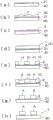
FIG. 1: in fig. 1, (a) to (f) are process diagrams showing respective steps of the mask forming method according to the present invention.
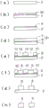
FIG. 2: in fig. 2, (a) to (h) are process diagrams showing respective steps of the method for manufacturing a printed wiring board by the subtractive method according to the present invention.
FIG. 3: in fig. 3, (a) to (h) are process diagrams showing respective steps of the method for manufacturing a printed wiring board by the semi-additive method according to the present invention.
FIG. 4: in fig. 4, (a) to (h) are process diagrams showing respective steps of the method for producing an electroformed component according to the present invention.
FIG. 5: in fig. 5, (a) to (f) are process diagrams showing respective steps of the method for manufacturing a screen printing plate according to the present invention.
Detailed Description
Embodiments according to the present invention will be described below with reference to the drawings.
Fig. 1 is a schematic view of a method of forming a mask 10, fig. 2 and 3 are schematic views showing a process for manufacturing a printed wiring board 4 by using the method of forming the mask 10 shown in fig. 1, and fig. 4 is a schematic view showing a process for manufacturing an electroformed component 5 by using the method of forming the mask 10 shown in fig. 1.
That is, the method of forming the mask 10 according to the present invention: a step of bringing an acidic aqueous solution 30 containing an undercoat layer forming agent into contact with the surface of the base material layer 2 to remove the oxide film 2a on the surface of the base material layer 2 and form an undercoat layer 3 derived from the undercoat layer forming agent on the exposed active surface of the base material layer 2 (fig. 1(a) to 1 (d)); a step of forming an ultraviolet-curable mask layer 31 composed of the primer layer 3 and the resin layer 1 by pressure-bonding a dry film, which is the resin layer 1 cured by irradiation, to the surface of the primer layer 3 at room temperature, and bonding the resin layer 1 to the surface of the base layer 2 via the primer layer 3; after the mask layer 31 is irradiated with an irradiation beam to cure the irradiated portion, the uncured mask layer 31 is removed to form a cured mask 10 (fig. 1(e) and 1 (f)).
As the above-mentioned base material layer 2, a layer of a metal selected from the group consisting of copper or an alloy containing copper, iron or an alloy containing iron, nickel or an alloy containing nickel, aluminum or an alloy containing aluminum, zinc or an alloy containing zinc, lead or an alloy containing lead, cobalt or an alloy containing cobalt, tin or an alloy containing tin, titanium or an alloy containing titanium, silver or an alloy containing silver, gold or an alloy containing gold, or platinum or an alloy containing platinum is suitably used. In the case of the resin, the resin may be the same as the resin layer or may be a different type of resin. Specific examples thereof include polyester, epoxy resin, polyimide resin, phenol resin, Polybenzimidazole (PBI) resin, and the like. In the case of the inorganic material, ceramics, glass, quartz, and the like can be cited.
The copper alloy is not particularly limited as long as it contains copper (Cu), and a copper alloy containing copper (Cu) as a main component and 1 or 2 or more of components such as Al, Mn, Fe, Sn, Mo, V, Pd, and Ta is particularly preferable according to the purpose.
The aluminum alloy is not particularly limited as long as it contains aluminum, and examples thereof include an ACL (Al-Co-Ge-La) alloy, an ACX (Al-Ni-B) alloy, an aluminum-neodymium (Al-Nd) alloy, an aluminum-zirconium (Al-Zr) alloy, an aluminum-copper (Al-Cu) alloy, an aluminum-silicon (Al-Si) alloy, and an aluminum-silicon-copper (Al-Si-Cu) alloy.
The iron alloy is not particularly limited as long as it contains iron (Fe), and particularly, an iron alloy containing iron (Fe) as a main component and 1 or 2 or more of components such as Ni, Cr, W, Cu, Co, C, Si, Mn, Mo, and the like according to the purpose is preferable, and specifically, products formed from a raw material such as ferritic stainless steel, martensitic stainless steel, austenitic stainless steel, or carbon steel are exemplified.
Among them, the acidic aqueous solution 30 containing the primer layer 3 forming agent preferably contains nitric acid or sulfuric acid. The ratio of the nitric acid to the whole acidic aqueous solution 30 is preferably adjusted to a range of 0.5 to 9.9 wt%, and the ratio of the sulfuric acid to the whole acidic aqueous solution 30 is preferably adjusted to a range of 0.5 to 9.9 wt%. As described above, if the concentration of nitric acid or sulfuric acid is less than 0.5 wt% based on the whole acidic aqueous solution 30, the concentration is too small to obtain the desired effect, while if the concentration of nitric acid or sulfuric acid exceeds 9.9 wt% based on the whole acidic aqueous solution 30, the concentration is too large, which is not only meaningless in blending, but also deteriorates safety, handleability, and working environment, and thus both cases are not preferable. Among these, it is preferable that the total amount of nitric acid and sulfuric acid is 9.9 wt% or less based on the entire acidic aqueous solution 30, because the acidic aqueous solution 30 is not a target of a so-called poison and violent poison association method, and transportation and storage are not restricted by various methods, and handling can be easily performed.
In the present invention, phosphoric acid may be added to the acidic aqueous solution as needed, and in this case, the amount of phosphoric acid to be added is preferably adjusted to a range of 0.05 to 40 wt%, and more preferably 0.5 to 25 wt%, with respect to the entire acidic aqueous solution 30, from the viewpoints of the effect, safety, handling properties, working environment, and the like.
Alternatively, in the above-mentioned acidic aqueous solution 30, an acidic aqueous solution containing three components of nitric acid, sulfuric acid and phosphoric acid is preferable, and in this case, it is preferable that the mixing ratio of nitric acid is in the range of 0.5 to 9.9 wt%, the mixing ratio of sulfuric acid is in the range of 0.5 to 9.9 wt% and the mixing ratio of phosphoric acid is in the range of 0.05 to 40 wt% in the entire acidic aqueous solution 30, and in this case, it is preferable that the total amount of nitric acid and sulfuric acid is 9.9 wt% or less with respect to the entire acidic aqueous solution 30, and by adjusting in this way, the acidic aqueous solution 30 is no longer a target of a so-called toxic and violent association method, and can be handled easily without being regulated by various methods in transportation and storage.
In the present invention, it is preferable that "hydrochloric acid" is further added to the acidic aqueous solution 30 so that hydrochloric acid is added to at least 1 selected from nitric acid and sulfuric acid to form a two-component acidic aqueous solution or a three-component acidic aqueous solution, or phosphoric acid is further added to form a three-component or four-component acidic aqueous solution 30, whereby the oxide film on the surface of the base material layer 2 can be suitably removed even for the base material layer 2 made of a nickel-containing alloy such as austenitic stainless steel.
The concentration of the hydrochloric acid to be further added to the acidic aqueous solution 30 is preferably in the range of 0.1 to 9.9 wt% with respect to the entire acidic aqueous solution 30, and if the concentration of the hydrochloric acid is less than 0.1 wt% with respect to the entire acidic aqueous solution 30, the concentration is too small to obtain the desired effect, while if the concentration of the hydrochloric acid exceeds 9.9 wt% with respect to the entire acidic aqueous solution 30, the meaning of the addition is lost, and too much causes deterioration in safety, handleability, and working environment, and therefore, neither case is preferable.
Further, in the above-mentioned acidic aqueous solution 30, when a mixed acid composed of 2 or more of hydrochloric acid, nitric acid and sulfuric acid is prepared, it is preferable that the total concentration of the mixed acid is 9.9 wt% or less with respect to the entire acidic aqueous solution 30, and by adjusting in this way, the acidic aqueous solution 30 is no longer an object of the toxic substance and the violent toxic substance association method, and is not subjected to various regulations with respect to transportation and storage, and can be easily handled, and therefore, it is more preferable.
In the present invention, the acidic aqueous solution 30 is mixed with an undercoat layer forming agent, and the undercoat layer forming agent is not particularly limited as long as it is a substance that, when the oxidized film 2a on the surface of the base material layer 2 is dissolved and removed by the acidic aqueous solution 30 to activate the surface of the base material layer 2, elemental ions that constitute a component of the base material layer 2 that is generated on the active surface bond with the undercoat layer forming agent to form the undercoat layer 3 on the surface of the base material layer 2.
Further, by forming the undercoat layer 3 on the active surface of the base material layer 2, oxidation of the active surface can be prevented.
The primer layer forming agent capable of forming the primer layer 3 includes a functional group such as a carboxyl group which can be easily bonded to an element ion constituting a component of the substrate layer 2 formed on the active surface of the substrate layer 2, and an organic group having good adhesion to the resin layer 1 formed on the active surface of the substrate layer 2.
Specific examples of the primer forming agent include at least 1 or more selected from gallic acid, pyrogalloc acid, tannic acid, citric acid, malic acid, lactic acid, tartaric acid, glycolic acid, glyceric acid, hydroxypentanoic acid, salicylic acid, mandelic acid, oxalic acid, malonic acid, succinic acid, glutaric acid, adipic acid, maleic acid, phthalic acid, or an alkali metal salt or an ammonium salt thereof, or an alkali metal salt or an ammonium salt of EDTA.
In the present invention, in the undercoat layer forming agent, the functional group thereof is mainly bonded to the ion of the element constituting the component of the base material layer 2 to form a compound, while the organic group faces the outside of the active surface of the base material layer 2, so that the adhesion between the undercoat layer 3 formed on the active surface of the base material layer 2 and the resin layer 1 is further improved.
The formation of the undercoat layer 3 may be performed using the one-pack type acidic aqueous solution 30 containing the undercoat layer forming agent as described above, or alternatively, the substrate layer 2 may be first treated with an acidic aqueous solution not containing the undercoat layer forming agent, and then treated with an aqueous solution containing the undercoat layer forming agent to perform a treatment with a two-pack type aqueous solution.
In the present invention, when the treatment is performed using the two-liquid type aqueous solution, first, the 1 st acidic aqueous solution containing the inorganic acid is brought into contact with the surface of the base material layer 2 to remove the oxide film 2a on the surface of the base material layer 2 and activate the surface of the base material layer 2.
Next, the active surface of the obtained base material layer 2 is brought into contact with a 2 nd aqueous solution containing an undercoat layer forming agent, and an undercoat layer 3 is formed on the active surface of the base material layer 2.
As the 2 nd aqueous solution, any of acidic, neutral or basic aqueous solutions can be used.
In the present invention, other components such as an organic acid and a surfactant may be appropriately added to the acidic aqueous solution (including the 1 st acidic aqueous solution and the same applies hereinafter) or the 2 nd aqueous solution, as required.
The "organic acid" is not particularly limited as long as it is an acid mainly used for preventing excessive dissolution of the surface of the base material layer 2, and an organic acid having a carboxyl group (-COOH) is generally preferred, and specific examples thereof include polyhydroxymonocarboxylic acid, gluconic acid, formic acid, acetic acid, propionic acid, butyric acid, and the like.
The amount of the organic acid added is appropriately determined depending on the material of the substrate layer 2 to be the object, the composition of the inorganic acid, and the like, and is not particularly limited, but is generally preferably in the range of 0.01 to 20.0 wt%, and more preferably about 0.1 to 10 wt% with respect to the whole acidic aqueous solution.
If the amount of the organic acid added is less than 0.01 wt% based on the whole acidic aqueous solution, the effect of suppressing the reaction of the base layer 2 is insufficient, and the desired suppression effect cannot be obtained, which is not preferable, while if the amount added exceeds 20.0 wt% based on the whole acidic aqueous solution, the effect is limited, which is not only meaningless, but also the balance with other components and the adjustment are deteriorated, and it becomes uneconomical, which is not preferable.
These organic acids may be added not only as one kind, but also as a mixture of two or more kinds as appropriate.
The "surfactant" is added mainly to allow an acidic aqueous solution to permeate and be compatible with the entire fine portion of the surface of the base material layer 2, to achieve a uniform treatment and to impart glossiness, and any of an anionic surfactant, a cationic surfactant, a nonionic surfactant, an amphoteric surfactant, and a nonionic surfactant can be used.
Specifically, examples of the anionic surfactant include fatty acid salt type, alkylbenzene sulfonate type, alkyl sulfate type, linear secondary sulfonate type, dialkyl sulfosuccinate type, POE alkyl or alkylphenyl ether sulfate type, POE alkyl or alkylphenyl ether phosphate type, and the like.
On the other hand, as the cationic surfactant, there can be mentioned an alkyl picolinium chloride type (アルキルピコリニウムクロライド), an alkyl triethylammonium chloride type, and other quaternary ammonium salt types.
Examples of the nonionic surfactant include POE alkylphenyl ether type nonionic, POE alkyl ether type nonionic, POE polyoxypropylene block polymer type nonionic, POE ethylene glycol alkyl ester type nonionic, sorbitan fatty acid ester type nonionic, and sucrose fatty acid ester type nonionic.
Further, examples of the amphoteric surfactant include alkylcarboxybetaine type, alkylaminocarboxylic acid type, and alkylimidazoline type.
Examples of the nonionic surfactant include POE alkyl ethers, POE alkylphenyl ethers, sucrose fatty acid esters, ethylene glycol, glycerin, and the like.
The amount of the surfactant to be added is appropriately determined depending on the raw material of the substrate layer 2 to be the object, the concentration of the inorganic acid, and the like, and is not particularly limited, but is generally preferably about 0.005 to 7.5% by weight, more preferably about 0.05 to 5% by weight, and particularly preferably about 0.1 to 3% by weight, based on the whole acidic aqueous solution.
If the amount of the surfactant added is less than 0.005% by weight based on the whole acidic aqueous solution, the amount of the surfactant added is too small to obtain the desired effect of addition, and therefore, it is not preferable, and if it exceeds 7.5% by weight, the effect is limited, and therefore, it is not only meaningless, but also in the case of performing the drainage treatment of the acidic aqueous solution, the waste liquid foams, and the treatment and adjustment thereof become difficult and become uneconomical, and therefore, it is not preferable.
The surfactant may be added not only in one kind but also in a mixture of two or more kinds as appropriate.
Next, in the present invention, a method for forming a mask will be described in detail.
As shown in fig. 1(a) to 1(c), the acidic aqueous solution 30 is brought into contact with the surface of the base material layer 2 to remove the oxide film 2a formed on the surface of the base material layer 2. As a method of contacting the substrate layer 2, the substrate layer may be immersed in the acidic aqueous solution 30 to be contacted, or the acidic aqueous solution may be contacted by any method such as coating, blowing, spreading, roll coating, or flooding (かけ flow し). In this case, if the oxidized film 2a on the surface of the base material layer 2 is removed to activate the surface of the base material layer 2, the elemental ions of the component constituting the base material layer 2 generated on the active surface thereof are bonded to the undercoat layer forming agent to form the undercoat layer 3 on the surface of the base material layer 2.
As shown in fig. 1(d), after the primer layer 3 is formed on the surface of the base material layer 2, the surface of the base material layer 2 is washed with water and dried. At this time, the active surface of the base layer 2 is protected by the undercoat layer 3, so that oxidation thereof is prevented, and adhesion between the base layer 2 and the undercoat layer 3 becomes extremely good. In this drying, if excessive heating is performed, the undercoat layer 3 may be thermally decomposed, and therefore, it is necessary to control the drying temperature. The drying conditions are not particularly limited, and specifically, the drying temperature is preferably controlled to be 100 ℃ or lower, preferably within a temperature range of room temperature to 55 ℃, particularly preferably within a temperature range of room temperature to 45 ℃, and the drying is preferably performed by a method such as natural drying, vacuum drying, heat drying, air drying, or hot air drying.
Next, as shown in fig. 1(e), a resin layer 1 cured by irradiation with radiation, in this case, ultraviolet rays, is provided on the surface of the dried undercoat layer 3, and the resin layer 1 is laminated on the surface of the base material layer 2 via the undercoat layer 3, thereby forming an ultraviolet-curable mask layer 31 composed of the undercoat layer 3 and the resin layer 2. The primer layer 3 is formed in a state of being adhered to the surface of the base layer 2, and the primer layer 3 has good compatibility with the resin layer 1, so that the adhesion with the resin layer 1 is remarkably improved.
In the present embodiment, the ultraviolet-curable mask layer 31 may be formed by bringing an ultraviolet-curable resin solution or an ultraviolet-curable resin solution into contact with the primer layer 3 on the surface of the base layer 2 and drying the same, or the ultraviolet-curable mask layer 31 may be formed by pressing an ultraviolet-curable dry film (resin layer 1) at room temperature or, if necessary, with heating. In the bonding of the dry film (resin layer 1), since the primer layer 3 is formed on the surface of the base material layer 2, the bonding property with the dry film (resin layer 1) is good, and as a result, the dry film (resin layer 1) can be effectively bonded to form the mask layer 31 even in a safe temperature range in a factory, that is, at room temperature or at a relatively low temperature (20 to 45 ℃). When the mask layer 31 is formed at a relatively low temperature in this manner, the mask layer 10 having a fine and precise pattern can be formed in a subsequent step as will be described later.
Further, as shown in fig. 1(f), after the ultraviolet-curable mask layer 31 is formed, a predetermined portion is irradiated with ultraviolet light from the mask layer, and the irradiated portion of the ultraviolet light is cured to form the mask layer 10. The treatment with ultraviolet rays may be performed by providing a pattern sheet having a pattern formed of an ultraviolet-ray irradiated portion and a non-irradiated portion on the surface of the mask layer 31 and irradiating ultraviolet rays therefrom, or may be performed by irradiating a predetermined portion of the mask layer 31 with ultraviolet rays in accordance with a previously programmed pattern and curing the pattern.
After the ultraviolet-curable mask layer 31 is cured in this way, the uncured part of the mask layer 31 is removed with a special solvent, and the mask layer 10 cured in a predetermined pattern is formed. In this case, since the mask layer 31 is formed at a relatively low temperature as described above, wrinkles, floating, further elongation, deformation, further gaps, and the like of the resin layer 1 do not exist, and thus the mask 10 having a fine, precise, and highly reliable pattern can be formed.
Next, a process for manufacturing the printed wiring board 4 by using the method for forming the mask 10 will be described.
Fig. 2 shows a process for manufacturing the printed wiring board 4 by the subtractive method.
As shown in fig. 2, in the method for manufacturing the printed wiring board 4, the surface of the metal layer (base material layer) 22 provided on the insulating layer 40 via the metal seed layer (base material layer) 21 is provided with the primer layer 3 formed by the above-described method using the acidic aqueous solution 30 containing the primer layer forming agent, and the ultraviolet-curable resin layer 1 is provided on the primer layer 3, thereby forming the ultraviolet-curable mask layer 31 (fig. 2a to 2 e). Then, a predetermined portion (the mask layer 10) where the mask layer 31 is cured and uncured portions other than the predetermined portion are formed by irradiating the predetermined portion with ultraviolet rays from above the mask layer 31.
Next, after the uncured portions of the mask layer 31 are removed with a solvent to expose the metal seed layer 21 and the metal layer 22 (fig. 2 f), the exposed metal seed layer 21 and the exposed metal layer 22 are removed with a solvent to form a conductive pattern a composed of the metal seed layer 21a and the metal layer 22a under the mask layer 10 (fig. 2 g and 2 h), and the mask layer 10 is removed to obtain the printed wiring board 4.
The method of manufacturing the printed wiring board 4 will be described in more detail.
As shown in fig. 2(a), a metal seed layer 21 is provided on the insulating layer 40.
The insulating layer 40 may be a rigid substrate such as a phenol resin paper substrate, an epoxy resin paper substrate, a glass composite substrate, a glass epoxy resin substrate, a fluororesin or a ceramic substrate, a flexible substrate made of a film of polyimide, polyester or the like, or a composite substrate of these.
When the metal layer 22 is formed on the surface of the insulating layer 40, a metal seed layer 21 is provided on the surface of the insulating layer 40 in order to improve adhesion between the insulating layer 40 and the metal layer 22. The metal seed layer 21 is made of Ni, Ni — Cr, Cu, or the like. The metal seed layer 21 is provided by physical vapor deposition, chemical vapor deposition, sputtering, or the like.
As shown in fig. 2(b), a metal layer 22 is provided on the surface of the metal seed layer 21. The metal layer 22 is formed of a conventionally known metal, specifically, a metal such as copper, a copper alloy, nickel, aluminum, zinc, tin, stainless steel, titanium, silver, gold, or an alloy thereof, since it is to be the conductor pattern a later. The metal layer 22 is formed by a known method such as plating.
Next, as shown in fig. 2(c) and (d), after the undercoat layer 3 is formed on the surface of the metal layer 22 using an acidic aqueous solution 30 containing an undercoat layer forming agent, the surface is washed with water and dried, and then, as shown in fig. 2(e), an ultraviolet-curable resin layer 1 is provided on the undercoat layer 3, thereby forming an ultraviolet-curable mask layer 31. In this case, the adhesion between the metal layer 22 and the mask layer 31 is extremely good through the undercoat layer 3.
Further, as shown in fig. 2(f), a predetermined portion of the mask layer 31 is irradiated with ultraviolet rays to cure the predetermined portion, and the uncured portion is removed with a solvent to form a cured mask layer 10. In this case, the treatment with ultraviolet rays may be performed by irradiating ultraviolet rays to cure only the ultraviolet-transmitting part of the original photographic plate on which the conductive pattern a is formed on the mask layer 31, or by irradiating ultraviolet rays to form the conductive pattern a in accordance with a previously programmed conductive pattern a. In this way, the mask layer 31 is irradiated with ultraviolet rays in a predetermined pattern to form a cured mask layer 10 portion and uncured portions other than the cured mask layer 10 portion, and then the uncured portions are removed with a solvent.
Then, as shown in fig. 2(g), if the exposed metal seed layer 21 and metal layer 22 are etched and removed, a conductor pattern a composed of the metal seed layer 21a and metal layer 22a existing below the cured mask layer 10 is formed.
Finally, as shown in fig. 2(h), the cured mask layer 10 is removed, and the printed wiring substrate 4 is completed.
The printed wiring board 4 thus formed has the metal layer 22 formed through the undercoat layer 3 formed on the metal seed layer 21, and the resin layer 1 is further bonded to the metal layer 22 without any gap and without any occurrence of elongation, shrinkage, deformation, and the like, and as a result, high density and high precision of the conductor pattern can be achieved, and a printed wiring board having a highly reliable fine conductor pattern can be easily obtained.
In the present embodiment, the printed wiring board 4 has been described as a single-sided board having the conductor pattern a formed on one side thereof, but may be a double-sided board.
Fig. 3 shows a process for manufacturing the printed wiring board 4 by the semi-additive method.
In the method for manufacturing the printed wiring board 4, the ultraviolet-curable resin layer 1 is provided through the undercoat layer 3 by using the acidic aqueous solution 30 containing the undercoat layer forming agent on the surface of the metal seed layer 21 provided on the insulating layer 40, and the ultraviolet-curable mask layer 31 is formed (fig. 3 a to 3 d).
Then, a predetermined portion (mask layer 10) where the mask layer 31 is cured and an uncured portion 11 other than the predetermined portion are formed by irradiating a predetermined portion with ultraviolet rays from above the ultraviolet-curing mask layer 31. Next, after the uncured portions 11 of the mask layer 31 are removed with a solvent to expose the metal seed layer 21 (fig. 3 e), a plating process is performed on the exposed metal seed layer 21 to form a conductor pattern a (fig. 3 f), and the cured mask layer 10 and the metal seed layer 21 thereunder are removed to form the conductor pattern a, thereby obtaining the printed wiring board 4 (fig. 3g and 3 h).
The metal seed layer 21 used in the present invention may be a metal layer having a one-layer structure or a metal layer having a 2-layer structure. The acidic aqueous solution 30 containing the undercoat layer forming agent used in the semi-additive method includes the same acidic aqueous solution as that used in the subtractive method.
In the printed wiring board 4 thus manufactured, as in the case of employing the subtractive method described above, the resin layer 1 is firmly adhered to the metal seed layer 21 via the undercoat layer 3 without any gap and without any occurrence of elongation, shrinkage, deformation, or the like, and as a result, high density and high precision of the conductor pattern can be achieved, and a printed wiring board having a highly reliable fine conductor pattern can be easily obtained.
Particularly, in the case of the semi-additive method, if the adhesion between the metal seed layer 21 and the mask layer 10 obtained by curing the ultraviolet-curable resin layer 31 is poor, the pattern 11 formed by the mask layer 10 may be subjected to plating treatment, which may cause the following problems: the mask 10 is peeled off and causes generation of a defective product, but if the method of the present invention is employed, generation of such a defective product can be prevented, and the yield of the product can be improved.
In the present embodiment, the printed wiring board 4 is also described as a single-sided board on one side of which the conductor pattern a is formed, but may be a double-sided board.
Fig. 4 shows a manufacturing process of the electroformed component 5.
In the method for producing the electroformed member 5, the undercoat layer 3 is formed on the surface of the base layer 2 by the above-described method using the acidic aqueous solution 30 containing the undercoat layer forming agent, and the ultraviolet-curable resin layer 1 is provided on the undercoat layer 3, thereby forming the ultraviolet-curable mask layer 31 (fig. 4 a to 4 d). In this case, the substrate layer 2 may be formed of a conventionally known metal, resin, or inorganic material.
Next, a predetermined portion (mask layer 10) where the mask layer 31 is cured and an uncured portion other than the predetermined portion are formed by irradiating a predetermined portion with ultraviolet rays from above the mask layer 31, and then the uncured portion of the mask layer 31 is removed with a solvent to expose the base material layer 2 and form the mold portion 12 (fig. 4 (e)).
Next, as shown in fig. 4(f) and 4(g), the electroforming part 5 is manufactured by applying electroforming plating treatment to the mold part 12. In the next step, the electroformed component 5 is obtained by heating or cooling the substrate, imparting a temperature difference with the temperature immediately after the production of the electroformed component 5, improving the releasability between the cured mask layer 10 and the electroformed component 5 by expansion or contraction of the mask layer 10 and the electroformed component 5, and then separating the cured mask layer 10 and the electroformed component 5 (fig. 4 (h)). The heating temperature is preferably in the range of 50-250 ℃ or the cooling temperature is preferably in the range of-5 ℃ to-200 ℃, and liquid nitrogen can be used according to the requirement. Alternatively, in order to improve the peelability of the electroformed component 5, it is preferable to control the temperature difference from immediately after the production of the electroformed component 5 to be about 150 to 250 ℃.
In the production of the electroformed component 5, the ultraviolet-curable resin layer 1 is formed on the base layer 2 via the undercoat layer 3 in a tightly adhered state without any gap. In this case, the resin layer 1 is firmly adhered to the undercoat layer 3 without being elongated or shrunk, and further without being deformed, and as a result, the electroformed component 5 having high density and high reliability with high accuracy can be easily obtained. Further, according to the method of the present invention, since the base material layer 2 and the mask 10 are firmly adhered to each other as described above, generation of defective products can be prevented, and the yield of products can be improved.
Fig. 5 shows a manufacturing process of the screen printing plate 6.
In the method for producing the screen printing plate-making 6, the acid aqueous solution 30 containing the primer layer forming agent is used to form the primer layer 3 on the surface of the screen printing mesh sheet 60 provided on the insulating layer 40 by the above-described method, and the ultraviolet-curable resin layer 1 is provided on the primer layer 3, thereby forming the ultraviolet-curable mask layer 31 (fig. 5 a to 5 d). In this case, the mesh sheet 60 may be a mesh sheet made of a conventionally known metal or resin.
Next, a predetermined portion (mask layer 10) where the mask layer 31 is cured and an uncured portion other than the predetermined portion are formed by irradiating a predetermined portion from the mask layer 31 with ultraviolet rays, and then the uncured portion of the mask layer 31 is removed with a solvent to expose the mesh sheet 60, thereby forming an opening 61 through which a paste (not shown) passes (fig. 5 (e)).
Next, as shown in fig. 5(f), if mesh sheet 60 is peeled off from insulating layer 40, and the top and bottom are reversed, screen printing plate making 6 is completed.
In the production of the screen printing plate 6, the ultraviolet-curable resin layer 1 is formed on the mesh sheet 60 through the undercoat layer 3 in a tightly adhered state without a gap, and the screen printing plate 6 is produced in this manner. In this case, the resin layer 1 is firmly adhered to the undercoat layer 3 without causing elongation, shrinkage, deformation, or the like, and as a result, the screen printing plate 6 having high density and high reliability and high accuracy can be easily obtained. Further, according to the method of the present invention, since the mesh sheet 60 is firmly adhered to the mask 10 as described above, generation of defective products can be prevented, and the yield of products can be improved.
Embodiments according to the present invention will be described below.
[ example 1]
As the acidic aqueous solution 30 containing the undercoat layer forming agent, an acidic aqueous solution 30 was prepared which was composed of 4.5 wt% of sulfuric acid, 2.0 wt% of hydrochloric acid, 1.1 wt% of tartaric acid, 0.9 wt% of pyrogalloc acid, 0.2 wt% of polyoxyethylene styrenated phenyl ether, and 91.3 wt% of water.
SUS304 (measured in SURF test SJ-301 manufactured by Mitutoyo Corporation, 50 mm. times.50 mm. times.t 1mm, average Ra0.05, RzJIS0.175) was used as a test substrate (substrate layer 2).
Next, the test substrate (substrate layer 2) was immersed in the acidic aqueous solution 30 containing the undercoat layer forming agent at a temperature of 25 ℃ for 3 minutes, then washed with pure water at a temperature of 25 ± 2 ℃ by spraying, and then dried by air blowing, to form the undercoat layer 3.
After the drying, an ultraviolet-curable dry film (フォトキャスト HM-4075 manufactured by hitachi chemical) as the resin layer 1 was laminated on the surface of the primer layer 3 of the test substrate (substrate layer 2) with the primer layer 3 under the temperature conditions shown in table 1 within 30 minutes.
That is, the test substrate (base material layer 2) was placed on a hot plate set to each predetermined temperature shown in table 1 for 5 minutes, and the dry film (resin layer 1) was bonded to the test substrate (base material layer 2). In this bonding, a stainless steel plate heated to each predetermined temperature in the same manner as the dry film (resin layer 1) was placed on the dry film, and the stainless steel plate was held for 5 minutes by its weight. In this case, the stainless steel sheet used was the same as the test substrate (base material layer 2), and the weight thereof was 18.3 g.
Through such steps, an ultraviolet-curable dry film (resin layer 1) is laminated on the surface of the test substrate (substrate layer 2) via the primer layer 3, thereby forming an ultraviolet-curable mask layer 31. Next, the entire surface of the ultraviolet-curable mask layer 31 was exposed to ultraviolet light for 5 minutes to be cured, and the cured mask layer 10 was formed on the entire surface to obtain a test piece.
In the mask layer 10 of the test piece thus obtained, cuts were formed at 5mm intervals in the vertical and horizontal directions, and a total of 25 meshes of 5 lines in the vertical and horizontal directions were formed. Then, a transparent tape (NICIBAN CO., manufactured by LTD., trade name CELLOTAPE CT1535) was attached to the surface of each mesh, and after rubbing the surface with a fingernail several times, the test substrate (substrate layer 2) and the tape were brought to an angle of 90 degrees, and an adhesion evaluation test by T-peeling was performed with a peel strength of 3N. The results are shown in table 1.
The adhesion evaluation criteria are as follows.
Evaluation criteria
Very good: 25-21 grids in 25 grids are defect-free
O: 20-13 grids in 25 grids are defect-free
And (delta): 12-6 grids in 25 grids are defect-free
X: no defect below 5 grids of 25 grids
The adhesion evaluation test using the transparent tape was performed 2 times, and the average value thereof was shown as the result. The temperature of the hot plate was 20 degrees, 30 degrees, 40 degrees, 50 degrees, 60 degrees, 70 degrees, 80 degrees, 90 degrees, and 100 degrees, respectively. The results are shown in table 1.
[ example 2]
A test piece was produced in the same manner as in example 1 using a tin plate having a thickness of 1mm as a test substrate (substrate layer 2), and using an acidic aqueous solution 30 containing an undercoat layer forming agent, instead of the acidic aqueous solution 30 used in example 1, the acidic aqueous solution 30 consisting of 4.5 wt% of sulfuric acid, 1.0 wt% of hydrochloric acid, 1.1 wt% of tartaric acid, 0.9 wt% of pyrogallol, 0.2 wt% of polyoxyethylene styrenated phenyl ether, and 92.3 wt% of water, and an adhesion evaluation test was performed in the same manner as in example 1. The results are shown in table 1.
Comparative example 1
A test piece was produced in the same manner as in example 1 except that an aqueous solution of mixed acid consisting of 4.5 wt% of sulfuric acid, 2.0 wt% of hydrochloric acid, 0.2 wt% of polyoxyethylene styrenated phenyl ether and 93.3 wt% of water was used instead of the acidic aqueous solution 30 containing the undercoat layer forming agent used in example 1, and an adhesion evaluation test was performed in the same manner as in example 1. That is, the test piece is prepared by directly bonding the dry film (resin layer 1) to the surface of the base material layer 2, and therefore, the evaluation of the adhesion is used to evaluate the adhesion between the base material layer 2 and the dry film (resin layer 1). The results are shown in table 1.
Comparative example 2
A test piece was produced in the same manner as in example 1 except that a hydrochloric acid mixed solution composed of 1.7 wt% of hydrochloric acid, 1.6 wt% of ferric chloride, 0.2 wt% of polyoxyethylene styrenated phenyl ether and 96.5 wt% of water was used instead of the acidic aqueous solution 30 containing the undercoat layer forming agent used in example 1, and an adhesion evaluation test was performed in the same manner as in example 1. That is, since the test piece is also prepared by directly bonding the dry film (resin layer 1) to the surface of the base material layer 2, the evaluation of the adhesion is performed to evaluate the adhesion between the base material layer 2 and the dry film (resin layer 1). The results are shown in table 1.
Comparative example 3
A test piece was produced in the same manner as in example 1 except that a nitric acid mixed solution consisting of 13.0 wt% of nitric acid, 15.8 wt% of ferric nitrate, 0.2 wt% of polyoxyethylene styrenated phenyl ether and 71.0 wt% of water was used instead of the acidic aqueous solution 30 containing the undercoat layer forming agent used in example 1, and an adhesion evaluation test was performed in the same manner as in example 1. That is, since the test piece is also prepared by directly bonding the dry film (resin layer 1) to the surface of the base layer 2, the evaluation of the adhesion is performed to evaluate the adhesion between the metal layer 2 and the dry film (resin layer 1). The results are shown in table 1.
Comparative example 4
Test pieces were prepared in the same manner as in example 1 except that a hydrogen peroxide-mixed acidic aqueous solution composed of 2.0% hydrogen peroxide, 9.0% sulfuric acid, 0.2% by weight of polyoxyethylene styrenated phenyl ether and 88.8% water was used instead of the acidic aqueous solution 30 containing the undercoat layer forming agent used in example 1, and adhesion evaluation tests were performed in the same manner as in example 1. That is, since the test piece is also prepared by directly bonding the dry film (resin layer 1) to the surface of the base material layer 2, the evaluation of the adhesion is performed to evaluate the adhesion between the base material layer 2 and the dry film (resin layer 1). The results are shown in table 1.
[ Table 1]

From the results shown in table 1, it was confirmed that: in each example, even at a relatively low temperature of about 20 ℃, the mask layer 10 having a desired adhesion can be formed on the surface of the undercoat layer 3 in the metal layer 2 having the undercoat layer 3.
On the other hand, it was confirmed that the required adhesion was not obtained in each comparative example even at a relatively high temperature of about 100 ℃.
[ example 3]
A test was carried out in the same manner as in example 1 except that immediately after the formation of the undercoat layer 3, the dry film was laminated at a hot plate temperature of 20 degrees (unheated room temperature) after 1 hour, 20 hours, 24 hours, and 72 hours of leaving at room temperature (20 ℃) after the formation of the undercoat layer 3. This adhesion evaluation test is used to evaluate the stability of the undercoat layer 3 and to evaluate how long it is possible to prevent oxidation of the active surface in the base material layer 2. The results are shown in table 2.
[ example 4]
A test was carried out in the same manner as in example 2 except that immediately after the formation of the undercoat layer 3, the dry film was laminated at a hot plate temperature of 20 degrees (unheated room temperature) after 1 hour, 20 hours, 24 hours, and 72 hours of leaving at room temperature (20 ℃) after the formation of the undercoat layer 3. The adhesion evaluation test evaluates the stability of the undercoat layer 3 to evaluate how long it is possible to prevent oxidation of the active surface in the base material layer 2. The results are shown in table 2.
Comparative example 5
The test was carried out in the same manner as in comparative example 1 except that the base material layer 2 was pretreated with an aqueous mixed acid solution, then washed with pure water at 25 ± 2 degrees by spraying, and then dried by air blowing immediately after drying, and after leaving at room temperature (20 ℃) for 1 hour, 20 hours, 24 hours, and 72 hours, respectively, the dry film was bonded at a hot plate temperature of 20 degrees (room temperature which was not heated). The adhesion evaluation test evaluates the stability of the active surface in the base material layer 2, and is used to confirm the degree to which the oxidation of the active surface in the base material layer 2 progresses with the passage of time and to confirm the change in adhesion between the base material layer 2 and the dry film (resin layer 1).
The results are shown in table 2.
Comparative example 6
The test was carried out in the same manner as in comparative example 2 except that the base material layer 2 was pretreated with an aqueous mixed acid solution, then washed with pure water at 25 ± 2 degrees by spraying, and then dried by air blowing immediately after drying, and after leaving at room temperature (20 ℃) for 1 hour, 20 hours, 24 hours, and 72 hours, respectively, the dry film was bonded at a hot plate temperature of 20 degrees (room temperature which was not heated). The adhesion evaluation test evaluates the stability of the active surface in the base material layer 2, and is used to confirm the degree to which the oxidation of the active surface in the base material layer 2 progresses with the passage of time and to confirm the change in adhesion between the base material layer 2 and the dry film (resin layer 1).
The results are shown in table 2.
Comparative example 7
The test was carried out in the same manner as in comparative example 3 except that the base material layer 2 was pretreated with an aqueous mixed acid solution, then washed with pure water at 25 ± 2 degrees by spraying, and then dried by air blowing immediately after drying, and after leaving at room temperature (20 ℃) for 1 hour, 20 hours, 24 hours, and 72 hours, respectively, the dry film was bonded at a hot plate temperature of 20 degrees (room temperature which was not heated). The adhesion evaluation test evaluates the stability of the active surface in the base material layer 2, and is used to confirm the degree to which the oxidation of the active surface in the base material layer 2 progresses with the passage of time and to confirm the change in adhesion between the base material layer 2 and the dry film (resin layer 1).
The results are shown in table 2.
Comparative example 8
The test was carried out in the same manner as in comparative example 4 except that the base material layer 2 was pretreated with an aqueous mixed acid solution, then washed with pure water at 25 ± 2 degrees by spraying, and then dried by air blowing immediately after drying, and after leaving at room temperature (20 ℃) for 1 hour, 20 hours, 24 hours, and 72 hours, respectively, the dry film was bonded at a hot plate temperature of 20 degrees (room temperature which was not heated). The adhesion evaluation test evaluates the stability of the active surface in the metal layer 2, and is used to confirm the degree to which the oxidation of the active surface in the base material layer 2 progresses with the passage of time and to confirm the change in adhesion between the base material layer 2 and the dry film (resin layer 1). The results are shown in table 2.
[ Table 2]

From the results shown in table 2, it was confirmed that: in each example, the primer layer 3 was formed on the surface of the stainless steel base material (base material layer 2), and even when 3 days or more elapsed from immediately after the formation of the primer layer 3, the dry film (resin layer 1) was firmly bonded to the stainless steel base material (base material layer 2) in an adhesive state.
In contrast, it was confirmed that each comparative example did not obtain the required adhesion immediately after the formation of the active surface of the base material layer 2, and the adhesion was deteriorated with time.
[ examples 5 and 6]
In example 5 or example 6, test pieces were produced in the same manner as in example 1 except that in example 5 or example 6, corresponding to example 1 or example 2, the base material layer 2 used in example 1 or example 2 was used instead of the copper plate as the test base material (50mm × 50mm × t1mm, average ra0.07, rzjis 0.35: measured in SURF test SJ-301 manufactured by Mitutoyo Corporation), and in example 5, the same acidic aqueous solution as in example 1 was used as the acidic aqueous solution, and in example 6, the same acidic aqueous solution as in example 2 was used, and the same adhesion evaluation test as in example 1 was performed.
The results are shown in table 3.
Comparative examples 9 to 12
In comparative examples 9 to 12, test pieces were produced in the same manner as in comparative example 1 except that in each of comparative examples 1 to 4, the base material layer 2 used in each of comparative examples 1 to 4 was replaced with a copper plate (50mm × 50mm × t1mm, average ra0.07, rzjis 0.35: measured in SURF test SJ-301 manufactured by Mitutoyo Corporation) as a test base material, and as an acidic aqueous solution, the same acidic aqueous solution as in comparative example 1 was used in comparative example 9, the same acidic aqueous solution as in comparative example 2 was used in comparative example 10, the same acidic aqueous solution as in comparative example 3 was used in comparative example 11, the same acidic aqueous solution as in comparative example 4 was used in comparative example 12, and the same adhesion evaluation test as in comparative example 1 was performed. The results are shown in table 3.
[ Table 3]

From the results shown in table 3, it was confirmed that: in each example, even at a relatively low temperature of about 20 ℃, the mask layer 10 having a desired adhesion can be formed on the surface of the undercoat layer 3 in the copper base material (base material layer 2) having the undercoat layer 3.
On the other hand, it was confirmed that in each comparative example, even at a relatively high temperature of about 90 ℃, the required adhesion was not obtained, and fluctuation was generated, and the reliability was poor in some cases.
[ examples 7 and 8]
In example 7 or example 8, the base material layer 2 used in example 3 or example 4 was replaced with a copper plate (50mm × 50mm × t1mm, average ra0.07, rzjis 0.35: measured in SURF test SJ-301 manufactured by Mitutoyo Corporation) as a test base material in accordance with example 3 or example 4, respectively, and as an acidic aqueous solution, the same acidic aqueous solution as in example 3 was used in example 7, the same acidic aqueous solution as in example 4 was used in example 8, the undercoat layer 3 was formed on the surface of the base material layer 2, respectively, and from immediately after the formation of the undercoat layer 3, after being left at room temperature (20 ℃) for 1 hour, 20 hours, 24 hours and 72 hours, an experiment was performed in the same manner as in example 3, except that the dry film was bonded at a hot plate temperature of 20 ℃ (room temperature). This adhesion evaluation test is used to evaluate the stability of the undercoat layer 3 and to evaluate how long oxidation of the active surface in the base material layer 2 can be prevented. The results are shown in table 4.
Comparative examples 13 to 16
In comparative examples 13 to 16, the base material layers 2 used in comparative examples 5 to 8 were used in place of copper plates (50mm × 50mm × t1mm, average ra0.07, rzjis 0.35: measured in SURF test SJ-301 manufactured by Mitutoyo Corporation) as test base materials, respectively, in addition, as an acidic aqueous solution, the same acidic aqueous solution as in comparative example 5 was used in comparative example 13, the same acidic aqueous solution as in comparative example 6 was used in comparative example 14, the same acidic aqueous solution as in comparative example 7 was used in comparative example 15, the same acidic aqueous solution as in comparative example 8 was used in comparative example 16, the primer layer 3 was not formed on the surface of the base material layer 2, and after the primer layer 3 was formed immediately thereafter, the base material layer was left at room temperature (20 ℃) for 1 hour, after 20 hours, after 24 hours, after 72 hours, and then the base material layers were bonded on a hot plate at a temperature of 20 ℃ (dry film heating room temperature), except for this, the test was performed in the same manner as in comparative example 5. The adhesion evaluation test evaluates the stability of the active surface in the substrate layer 2, and is used to confirm how much the oxidation of the active surface in the substrate layer 2 progresses with the passage of time and to confirm the change in adhesion between the substrate layer 2 and the dry film (resin layer 1). The results are shown in table 4.
[ Table 4]

From the results shown in table 4, it was confirmed that: in each example, the undercoat layer 3 is formed on the surface of the copper base material (base material layer 2), and even when 3 days or more have elapsed from immediately after the formation of the undercoat layer 3, the dry film (resin layer 1) can be firmly bonded to the copper base material (base material layer 2) in an adhesive state.
In contrast, it was confirmed that each comparative example did not obtain the required adhesion immediately after the formation of the active surface of the copper base material (base material layer 2), and the adhesion was deteriorated with time.
[ example 9]
A test piece was produced in the same manner as in example 1 except that a mixed acid aqueous solution composed of 4.5 wt% of sulfuric acid, 2.0 wt% of hydrochloric acid, 0.2 wt% of polyoxyethylene styrenated phenyl ether and 93.3 wt% of water was used, the same base material layer 2 as in example 1 was immersed in the mixed acid aqueous solution at a temperature of 25 ℃ for 3 minutes to remove an oxide film of the base material layer 2 and activate the surface thereof, and then treated with an acidic aqueous solution containing the following primer layer-forming agent to form a primer layer 3, and an adhesion evaluation test was performed in the same manner as in example 1. That is, while the above examples 1 to 8 use a one-pack type acidic aqueous solution containing an undercoat layer forming agent for treatment, the examples use a two-pack type aqueous solution for treatment.
The acidic aqueous solution containing the primer layer forming agent used in example 9 was composed of 0.25% by weight of hydrochloric acid, 1.1% by weight of tartaric acid, 0.9% by weight of pyrogalloc acid, 0.2% by weight of polyoxyethylene styrenated phenyl ether and 97.55% by weight of water. The results are shown in table 5.
[ example 10]
A test piece was produced in the same manner as in example 1 except that in the method of treating a two-liquid aqueous solution of example 9, instead of the hydrochloric acid aqueous solution containing an undercoat layer forming agent, a neutral aqueous solution of 2 wt% pyrogalloc acid and 98 wt% water was used to form an undercoat layer 3, and an adhesion evaluation test was performed in the same manner as in example 1. That is, in this case, the treatment is also performed using a two-liquid type aqueous solution. The results are shown in table 5.
[ example 11]
A test piece was produced in the same manner as in example 1 except that in the method of treating the two-liquid type aqueous solution of example 9, an alkaline aqueous solution consisting of 1.4 wt% of pyrogalloc acid, 4.8 wt% of sodium carbonate, 1.1 wt% of sodium hydroxide, and 92.7 wt% of water was used instead of the hydrochloric acid aqueous solution containing the primer layer forming agent to form the primer layer 3, and the adhesion evaluation test was performed in the same manner as in example 1. That is, in this case, the treatment is also carried out using a two-liquid type aqueous solution. The results are shown in table 5.
[ Table 5]

From the results shown in table 5, it was confirmed that: in each of examples 9 to 11, the mask layer 10 having the desired adhesion can be formed on the surface of the undercoat layer 3 in the base layer 2 having the undercoat layer 3 even at a relatively low temperature of about 20 ℃.
[ examples 12 to 14]
Tests were carried out in the same manner as in examples 1, 3, and 9, except that the raw material of the base layer 2 was changed to a phenol resin in examples 1, 3, and 9. All results obtained an evaluation of ". circinata".
In the present invention, since the resin layer such as a dry film can be pressed against the undercoat layer without heating, the resin layer can be formed neatly on the surface of the undercoat layer without causing elongation and shrinkage of the resin layer, further without causing deformation, further without causing floating, sagging, or the like, and as a result, high density and high precision of the conductor pattern can be achieved, and a printed wiring board and an electroformed component having a highly reliable fine conductor pattern can be obtained.
The present invention may be embodied in other various forms without departing from the spirit or essential characteristics thereof. Therefore, the above-described embodiments are merely illustrative in all aspects and should not be construed as limiting. The scope of the invention is indicated by the claims, and is not limited in any way by the text of the specification. Further, all modifications and variations falling within the equivalent scope of the claims are within the scope of the present invention.
Industrial applicability
In the present invention, as described above, high density and high precision of the conductor pattern can be achieved, and a printed wiring board and an electroformed component having a highly reliable fine conductor pattern can be obtained, and therefore, the present invention has an extremely high industrial utility value.
Description of reference numerals
1 ultraviolet-curable resin layer
10 cured mask (layer)
11 electroforming mold (mold part)
2 base material layer
21 Metal seed layer (substrate layer)
22 Metal layer (substrate layer)
3 base coat
30 acidic aqueous solution containing primer layer Forming agent
31 ultraviolet curing mask layer
4 printed wiring board
5 electroforming of parts
6 Screen printing plate making
60 mesh sheet (substrate layer)
61 opening part
A pattern
Claims (10)
1. A method for forming a mask, characterized in that,
a step of bringing an acidic aqueous solution containing an undercoat layer forming agent into contact with the surface of the base material layer to remove an oxide film on the surface of the base material layer and form an undercoat layer on the active surface of the base material layer exposed thereby;
a step of forming a mask layer composed of the undercoat layer and a resin layer by providing a resin layer cured by irradiation on the surface of the undercoat layer and laminating the resin layer on the surface of the base material layer through the undercoat layer; and
irradiating a predetermined portion of the mask layer with an irradiation ray to cure the irradiated portion, and then removing the uncured mask layer to form a cured mask layer;
wherein,
the substrate layer is a layer of metal selected from copper or copper-containing alloy, iron or iron-containing alloy, nickel or nickel-containing alloy, aluminum or aluminum-containing alloy, cobalt or cobalt-containing alloy, tin or tin-containing alloy, titanium or titanium-containing alloy, silver or silver-containing alloy, gold or gold-containing alloy, or platinum-containing alloy, and is polyester, epoxy resin, polyimide resin, phenolic resin-Polybenzimidazole (PBI) resin, or is ceramic, glass, or quartz;
the acidic aqueous solution is:
4.5% by weight of sulfuric acid, 2.0% by weight of hydrochloric acid, 1.1% by weight of tartaric acid, 0.9% by weight of pyrogallol, 0.2% by weight of polyoxyethylene styrenated phenyl ether and 91.3% by weight of water; or
4.5% by weight of sulfuric acid, 1.0% by weight of hydrochloric acid, 1.1% by weight of tartaric acid, 0.9% by weight of pyrogallol, 0.2% by weight of polyoxyethylene styrenated phenyl ether and 92.3% by weight of water.
2. A method for forming a mask, characterized in that,
bringing an acidic aqueous solution into contact with the surface of the base material layer to remove the oxide film on the surface of the base material layer and activate the surface of the base material layer;
forming an undercoat layer on the active surface of the base material layer by bringing an aqueous solution containing an undercoat layer forming agent into contact with the active surface of the base material layer;
a step of forming a mask layer composed of the undercoat layer and a resin layer by providing a resin layer cured by irradiation on the surface of the undercoat layer and laminating the resin layer on the surface of the base material layer through the undercoat layer; and
irradiating a predetermined portion of the mask layer with an irradiation ray to cure the irradiated portion, and then removing the uncured mask layer to form a cured mask layer;
wherein,
the substrate layer is a layer of metal selected from copper or copper-containing alloy, iron or iron-containing alloy, nickel or nickel-containing alloy, aluminum or aluminum-containing alloy, cobalt or cobalt-containing alloy, tin or tin-containing alloy, titanium or titanium-containing alloy, silver or silver-containing alloy, gold or gold-containing alloy, or platinum-containing alloy, and is polyester, epoxy resin, polyimide resin, phenolic resin-Polybenzimidazole (PBI) resin, or is ceramic, glass, or quartz;
the acidic aqueous solution is: 4.5% by weight of sulfuric acid, 2.0% by weight of hydrochloric acid, 0.2% by weight of polyoxyethylene styrenated phenyl ether and 93.3% by weight of water;
the primer forming agent is any one of an acidic aqueous solution containing 0.25 wt% of hydrochloric acid, 1.1 wt% of tartaric acid, 0.9 wt% of pyrogalloc acid, 0.2 wt% of polyoxyethylene styrenated phenyl ether and 97.55 wt% of water, a neutral aqueous solution containing 2.0 wt% of pyrogalloc acid and 98 wt% of water, or a basic aqueous solution containing 1.4 wt% of pyrogalloc acid, 4.8 wt% of sodium carbonate, 1.1 wt% of sodium hydroxide and 92.7 wt% of water.
3. The method of forming a mask according to claim 1 or 2, wherein the resin layer is a radiation-curable dry film.
4. The method of forming a mask according to claim 1 or 2, wherein the resin layer is formed by applying a radiation-curable resin solution or a resin solution to the surface of the base material layer and then drying the resin solution.
5. The method of forming a mask according to claim 1 or 2, wherein the undercoat layer is formed, dried at a temperature ranging from room temperature to 100 ℃ after washing, and then a resin layer cured by irradiation is provided on the surface of the dried undercoat layer.
6. The method of forming a mask according to claim 1 or 2, wherein the irradiation ray is infrared ray, near infrared ray, ultraviolet ray, electron beam, or laser.
7. A method for manufacturing a printed wiring board, characterized in that after a cured mask layer is formed by the method according to any one of claims 1 to 6 on the surface of a first base material layer made of a metal provided on an insulating layer or on the surface of a second base material layer made of a metal provided on an insulating layer via a metal seed layer, the metal seed layer not protected by the mask layer and the first base material layer made of a metal or the second base material layer made of a metal are removed, the metal seed layer protected by the mask layer and the first base material layer made of a metal or the second base material layer made of a metal are formed into a conductor pattern, and then the cured mask layer is removed.
8. A method for manufacturing a printed wiring board, characterized in that a cured mask layer is formed on the surface of a metal seed layer provided on an insulating layer by the method according to any one of claims 1 to 6, then the uncured part of the mask layer is removed to form a pattern, a plating treatment is applied to the pattern part to form a conductor pattern, and then the mask layer and the metal seed layer protected by the mask layer are removed.
9. A method for producing an electroformed component, comprising forming a cured mask layer by the method according to any one of claims 1 to 6, removing an uncured portion of the mask layer to form a mold section, subjecting the mold section to an electroforming plating treatment to form an electroformed component, heating or cooling the electroformed component to impart a temperature difference, improving the releasability between the cured mask layer and the electroformed component by expansion or contraction of the cured mask layer and the electroformed component, and then releasing the cured mask layer and the electroformed component.
10. A method for producing a screen printing plate, comprising forming a cured mask layer by the method according to any one of claims 1 to 6 using a base material layer as a mesh sheet for screen printing, and removing an uncured portion of the mask layer to form an opening through which a paste for screen printing passes.
Applications Claiming Priority (3)
| Application Number | Priority Date | Filing Date | Title |
|---|---|---|---|
| JP2015-087166 | 2015-04-21 | ||
| JP2015087166 | 2015-04-21 | ||
| PCT/JP2016/062057 WO2016171074A1 (en) | 2015-04-21 | 2016-04-15 | Method for forming mask, and method for manufacturing printed wiring board, method for manufacturing electroformed component, and method for manufacturing screen printing plate using same |
Publications (2)
| Publication Number | Publication Date |
|---|---|
| CN107533298A CN107533298A (en) | 2018-01-02 |
| CN107533298B true CN107533298B (en) | 2021-06-22 |
Family
ID=57144437
Family Applications (1)
| Application Number | Title | Priority Date | Filing Date |
|---|---|---|---|
| CN201680023007.2A Active CN107533298B (en) | 2015-04-21 | 2016-04-15 | Mask forming method and method for manufacturing printed wiring board using the same |
Country Status (4)
| Country | Link |
|---|---|
| JP (1) | JP6829859B2 (en) |
| CN (1) | CN107533298B (en) |
| TW (1) | TWI693485B (en) |
| WO (1) | WO2016171074A1 (en) |
Families Citing this family (4)
| Publication number | Priority date | Publication date | Assignee | Title |
|---|---|---|---|---|
| US20200087808A1 (en) * | 2016-12-23 | 2020-03-19 | 3M Innovative Properties Company | Method of electroforming microstructured articles |
| TWI651994B (en) * | 2018-03-06 | 2019-02-21 | 易華電子股份有限公司 | System for improving the stability of dry film and substrate |
| TWI669404B (en) * | 2018-06-06 | 2019-08-21 | 張東暉 | Metal evaporation mask structure |
| JP7478262B2 (en) * | 2020-12-24 | 2024-05-02 | 京セラ株式会社 | Screen printing plate making and screen printing equipment |
Citations (7)
| Publication number | Priority date | Publication date | Assignee | Title |
|---|---|---|---|---|
| JP2004058640A (en) * | 2002-07-29 | 2004-02-26 | Needs:Kk | Screen printing plate |
| CN1612048A (en) * | 2003-10-30 | 2005-05-04 | 富士胶片株式会社 | Method for making printed circuit board |
| CN1653873A (en) * | 2002-05-17 | 2005-08-10 | 独立行政法人科学技术振兴机构 | Method for forming multilayer circuit structure and base having multilayer circuit structure |
| JP2006235499A (en) * | 2005-02-28 | 2006-09-07 | Hitachi Chem Co Ltd | Photosensitive resin composition, photosensitive element using the same, resist pattern forming method, method for manufacturing printed wiring board and method for removing photoset object |
| JP2007334058A (en) * | 2006-06-15 | 2007-12-27 | Murata Mfg Co Ltd | Screen printing plate and method for manufacturing the same |
| JP2012237064A (en) * | 2011-04-28 | 2012-12-06 | Hokuriku Roka:Kk | Surface modification treatment agent and surface modification method |
| TW201433231A (en) * | 2012-12-14 | 2014-08-16 | Uyemura C & Co Ltd | Method for manufacturing a printed circuit board and a printed circuit board manufactured by using the same |
Family Cites Families (5)
| Publication number | Priority date | Publication date | Assignee | Title |
|---|---|---|---|---|
| JP2005039097A (en) * | 2003-07-16 | 2005-02-10 | Matsushita Electric Ind Co Ltd | Method for forming copper-foil wiring, wiring transfer substrate and wiring board |
| JP2006156605A (en) * | 2004-11-29 | 2006-06-15 | Matsushita Electric Works Ltd | Method for manufacturing multilayer circuit board |
| JP5232487B2 (en) * | 2007-02-22 | 2013-07-10 | 富士フイルム株式会社 | Planographic printing plate precursor and planographic printing method |
| KR20110118803A (en) * | 2009-04-20 | 2011-11-01 | 아사히 가세이 이-매터리얼즈 가부시키가이샤 | Photosensitive resin laminate |
| JP2014051575A (en) * | 2012-09-06 | 2014-03-20 | Tosoh Corp | Cleaning composition |
-
2016
- 2016-04-15 WO PCT/JP2016/062057 patent/WO2016171074A1/en active Application Filing
- 2016-04-15 CN CN201680023007.2A patent/CN107533298B/en active Active
- 2016-04-15 JP JP2016082149A patent/JP6829859B2/en active Active
- 2016-04-19 TW TW105112155A patent/TWI693485B/en active
Patent Citations (7)
| Publication number | Priority date | Publication date | Assignee | Title |
|---|---|---|---|---|
| CN1653873A (en) * | 2002-05-17 | 2005-08-10 | 独立行政法人科学技术振兴机构 | Method for forming multilayer circuit structure and base having multilayer circuit structure |
| JP2004058640A (en) * | 2002-07-29 | 2004-02-26 | Needs:Kk | Screen printing plate |
| CN1612048A (en) * | 2003-10-30 | 2005-05-04 | 富士胶片株式会社 | Method for making printed circuit board |
| JP2006235499A (en) * | 2005-02-28 | 2006-09-07 | Hitachi Chem Co Ltd | Photosensitive resin composition, photosensitive element using the same, resist pattern forming method, method for manufacturing printed wiring board and method for removing photoset object |
| JP2007334058A (en) * | 2006-06-15 | 2007-12-27 | Murata Mfg Co Ltd | Screen printing plate and method for manufacturing the same |
| JP2012237064A (en) * | 2011-04-28 | 2012-12-06 | Hokuriku Roka:Kk | Surface modification treatment agent and surface modification method |
| TW201433231A (en) * | 2012-12-14 | 2014-08-16 | Uyemura C & Co Ltd | Method for manufacturing a printed circuit board and a printed circuit board manufactured by using the same |
Also Published As
| Publication number | Publication date |
|---|---|
| TWI693485B (en) | 2020-05-11 |
| JP6829859B2 (en) | 2021-02-17 |
| WO2016171074A1 (en) | 2016-10-27 |
| CN107533298A (en) | 2018-01-02 |
| JP2016206670A (en) | 2016-12-08 |
| TW201702766A (en) | 2017-01-16 |
Similar Documents
| Publication | Publication Date | Title |
|---|---|---|
| CN107533298B (en) | Mask forming method and method for manufacturing printed wiring board using the same | |
| JP4126038B2 (en) | BGA package substrate and manufacturing method thereof | |
| JP5724468B2 (en) | Method for producing polyimide metal laminate | |
| US11266025B2 (en) | Electronic-component manufacturing method and electronic components | |
| TW200407061A (en) | Process for creating vias for circuit assemblies | |
| JPH01261888A (en) | Manufacture of printed board | |
| US5145553A (en) | Method of making a flexible circuit member | |
| JPH02173129A (en) | Method for surface treatment of polyimide to improve receptivity to metallic layer | |
| JP2016206670A5 (en) | ||
| JP6841585B2 (en) | Manufacturing method of laminated structure and laminated film | |
| JP2012182292A (en) | Resin opening method | |
| TW592009B (en) | Use of metallic treatment on copper foil to produce fine lines and replace oxide process in printed circuit board production | |
| NO141554B (en) | ANALOGICAL PROCEDURE FOR THE PREPARATION OF T.-AMINO-ALKYLPHENYL ESTERS WITH LOCAL ANESTHETIC EFFECT | |
| JP4900036B2 (en) | Resin substrate ozone solution processing method and wiring substrate manufacturing method | |
| JP6516367B2 (en) | Method of forming mask, method of manufacturing printed wiring board using the same, method of manufacturing electroformed part, and method of manufacturing screen printing plate making | |
| JP5246521B2 (en) | Manufacturing method of electronic parts adopting wet etching, electronic parts and hard disk suspension | |
| KR102138341B1 (en) | Film type antenna using high ductility nickel/stannum plating and its manufacturing method | |
| JP2015035331A (en) | Method for producing conductive coating film and conductive coating film | |
| JP5760162B2 (en) | Method for producing transparent conductive film | |
| JP6031332B2 (en) | Surface-treated copper foil, laminate using the same, printed wiring board, electronic component, and method for producing surface-treated copper foil | |
| JP2009295872A (en) | Method for manufacturing printed circuit board, and printed circuit board | |
| JP2531466B2 (en) | Method for manufacturing printed wiring board | |
| JPH03221449A (en) | Metal foil with ultraviolet cured water base resin, and metal coated laminate sheet with ultraviolet cured water base resin, and manufacture thereof and removing method of cured film thereof | |
| WO2006093272A1 (en) | Wiring substrate, manufacturing method thereof, and resin body surface treatment method | |
| WO2015087876A1 (en) | Electroless plating method |
Legal Events
| Date | Code | Title | Description |
|---|---|---|---|
| PB01 | Publication | ||
| PB01 | Publication | ||
| SE01 | Entry into force of request for substantive examination | ||
| SE01 | Entry into force of request for substantive examination | ||
| GR01 | Patent grant | ||
| GR01 | Patent grant |