Drawings
Fig. 1 is a schematic exploded perspective view illustrating a configuration of a display device manufactured based on an in-housing technique;
FIG. 2A illustrates workpiece preparation in a manufacturing process based on an overview of optical bonding off-housing technology;
FIG. 2B illustrates the dam ring (dam) application and curing in the manufacturing process based on the optical bonding outside the housing technique;
FIG. 2C illustrates OCR application in a manufacturing process based on optical bonding with out-of-housing technology;
FIG. 2D illustrates bonding of front panels in a manufacturing process based on optical bonding of out-of-housing technology;
FIG. 2E illustrates OCR temporary curing in a manufacturing process based on an overview of optical bonding off-housing technology;
FIG. 2F illustrates OCR full cure in the manufacturing process based on optical bonding outside the housing technology;
FIG. 3A illustrates workpiece preparation in a manufacturing process based on an overview of the technology within an optical bond enclosure;
FIG. 3B illustrates the dam ring application and curing in the manufacturing process based on the overview of the technology within the optical bond housing;
FIG. 3C illustrates OCR application in a manufacturing process based on optical bonding in-housing technology;
FIG. 3D illustrates bonding of a front panel in a manufacturing process based on optical bonding of in-housing technology;
FIG. 3E illustrates OCR temporary curing in a manufacturing process based on an overview of the technology within the optical bond housing;
FIG. 3F illustrates OCR full cure in the manufacturing process based on optical bonding in-housing technology;
fig. 4 is a schematic exploded perspective view illustrating a configuration of a display device manufactured based on an out-of-housing technique;
fig. 5 is a schematic exploded perspective view illustrating an example in which the shape of a resin tail ring changes along a boundary portion of a housing;
fig. 6A is a schematic sectional view illustrating a cross-sectional structure (a cross-section along VI-VI in fig. 1) of the display device;
fig. 6B is a schematic sectional view illustrating a cross-sectional structure (a cross-section along VI-VI in fig. 4) of the display device;
FIG. 7A is a schematic cross-sectional view illustrating UV non-illuminable regions in the art within an enclosure;
FIG. 7B is a schematic cross-sectional view illustrating UV non-illuminable regions in the out-of-housing technique;
FIG. 8A is a schematic cross-sectional view illustrating the location where a resin tail ring is formed in the housing technology;
FIG. 8B is a schematic cross-sectional view illustrating the location where a resin tail ring is formed in the housing technology;
fig. 9A is a schematic cross-sectional view illustrating a structure of holding upper and lower substrates based on the in-housing technique;
fig. 9B is a schematic cross-sectional view illustrating a structure of holding upper and lower substrates based on the out-of-housing technique;
fig. 10 is a schematic cross-sectional view illustrating separation of a resin tail ring due to a load;
fig. 11 is a schematic perspective view illustrating a protrusion at a tail ring engaging portion;
fig. 12A shows a schematic top view and a schematic side view illustrating the adaptability of the bulge at the striker ring engagement portion;
fig. 12B shows a schematic top view and a schematic side view illustrating the adaptability of the bulge at the striker ring engagement portion;
fig. 12C shows a schematic top view and a schematic side view illustrating the adaptability of the bulge at the striker ring engagement portion;
fig. 12D shows a schematic top view and a schematic side view illustrating the adaptability of the bulge at the striker ring engagement portion;
fig. 12E shows a schematic top view and a schematic side view illustrating the adaptability of the bulge at the striker ring engagement portion;
fig. 13A is a schematic cross-sectional view illustrating an example of a basic cross-sectional shape of a housing;
fig. 13B is a schematic cross-sectional view illustrating an example of the basic cross-sectional shape of the housing;
fig. 13C is a schematic cross-sectional view illustrating an example of the basic cross-sectional shape of the housing;
fig. 14A is a schematic cross-sectional view illustrating an example of the shape of a machined surface in corner finishing on a boundary portion of a housing;
fig. 14B is a schematic cross-sectional view illustrating an example of the shape of the machined surface in corner finishing on a boundary portion of the housing;
fig. 14C is a schematic cross-sectional view illustrating an example of the shape of the machined surface in corner finishing on the boundary portion of the housing;
fig. 14D is a schematic cross-sectional view illustrating an example of the shape of the machined surface in corner finishing on the boundary portion of the housing;
fig. 15 is a schematic partial sectional view illustrating the arrangement position and width (along the length of the inner edge of the outer shell) of the working face;
FIG. 16A shows a schematic enlarged perspective view and a schematic cross-sectional view of an example of a composite material illustrating corner processing performed on a border portion of the shell;
FIG. 16B shows a schematic enlarged perspective view and a schematic cross-sectional view of an example of a composite material illustrating corner processing performed on a border portion of the shell;
fig. 17A illustrates an example of the shape of a boundary portion of a housing in corner processing;
fig. 17B illustrates an example of the shape of a boundary portion of a housing in corner processing;
fig. 18 illustrates a schematic cross-sectional view of a display device;
fig. 19 is a schematic enlarged partial perspective view illustrating an example in which a portion of a resin tail ring engaging portion corresponding to a housing is provided with a corner treatment to have an inclined surface;
fig. 20 is a schematic enlarged partial perspective view illustrating an example in which a portion of a resin tail ring engaging portion corresponding to a housing is provided with a corner treatment to have an L-shaped surface;
fig. 21A shows a schematic top view and a schematic side view illustrating the adaptation of the bulge at the resin tail ring engaging portion;
fig. 21B shows a schematic top view and a schematic side view illustrating the adaptability of the bulge at the resin tail ring engaging portion;
fig. 21C shows a schematic top view and a schematic side view illustrating the adaptability of the bulge at the resin tail ring engaging portion;
fig. 21D shows a schematic top view and a schematic side view illustrating the adaptation of the bulge at the resin tail ring engaging portion;
fig. 21E shows a schematic top view and a schematic side view illustrating the adaptation of the bulge at the resin tail ring engaging portion;
fig. 22A is a schematic cross-sectional view illustrating an example of an unmodified shape of a resin tail ring in which there is a passage to a UV non-irradiation region;
fig. 22B is a schematic cross-sectional view illustrating an example of an unmodified shape of a resin tail ring in which there is a passage to a UV non-irradiation region;
fig. 22C is a schematic cross-sectional view illustrating an example of an unmodified shape of a resin tail ring in which there is a passage to a UV non-irradiation region;
fig. 23 is a schematic exploded perspective view illustrating the configuration of a display device according to embodiment 3; and
fig. 24 is a schematic sectional view illustrating a configuration of a display device according to embodiment 3.
Detailed Description
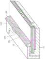
Fig. 1 is a schematic exploded perspective view illustrating the configuration of a display device manufactured based on the in-housing technology. A unit including upper and lower substrates 100 formed by adhering an upper substrate to a lower substrate, a case 101 supporting and accommodating the upper and lower substrates 100, and a housing 102 having a portion for display opened is referred to as a display module 103. The upper and lower substrates 100 correspond to a liquid crystal display panel, and include, for example, a Color Filter (CF) substrate and a Thin Film Transistor (TFT) substrate. The housing 101 is, for example, a backlight unit. The housing 102 is, for example, a metal bezel.
An exemplary display device includes a display module 103 having a display portion completely combined with a front panel 106 by an OCR104 as a transparent resin (see fig. 1). The front panel 106 is, for example, a projected capacitive touch panel (PCAP) or tempered glass.
In manufacturing such a display device, a method of forming a sealing material made of resin in a gap between the housing 102 and the upper and lower substrates 100 so that the OCR104 does not leak into the inside of the display module 103 before curing is adopted. For convenience, the formation of the sealing material is referred to as stock ring formation, the resin to be used is referred to as stock ring material, and the formed sealing portion is referred to as a resin stock ring (resin member) 105.
A basic manufacturing process based on the outside-housing technology is disclosed in patent document 1. A basic manufacturing process based on the in-housing technology is disclosed in patent document 2. Which manufacturing process (and product structure) to select depends on product specifications, development costs, business strategies, and the like. The present application is directed to solving problems in the art within a housing.
An outline of a manufacturing process in the case outside technology according to the comparative example is illustrated in fig. 2A to 2F. An overview of the manufacturing process in the in-housing technology is illustrated in fig. 3A to 3F. The configuration of a display device manufactured based on the out-of-housing technology is illustrated in fig. 4. The configuration of a display device manufactured based on the in-housing technology is illustrated in fig. 1.
An outline of a manufacturing process based on the out-of-case technology is described with reference to fig. 2A to 2F. As shown in fig. 2A, the display surfaces of the upper and lower substrates 100 corresponding to the workpiece are placed in a horizontal state, and preparation for the subsequent steps is made. As shown in fig. 2B, the dispenser 300 is used to apply the tail ring material with a single stroke along the perimeter of the upper and lower substrates 100. Here, a resin tail ring engaging portion 504 (see fig. 11) is also formed, in which a starting end 502 (see fig. 11) from which application is started and an ending end 503 (see fig. 11) at which application is completed overlap each other. Note that the application of the tail ring material may be repeated more than once. In this case, more than one resin tail ring engaging portion 504 is also formed. An ultraviolet lamp (UV lamp) 301 is used for UV irradiation to cure the dam material and form the resin dam 105.
As shown in fig. 2C, OCR104 is applied to the inside of the resin tail ring 105. The OCR104 is satisfactorily applied in a uniform thickness by using a dispenser 300 having a plurality of nozzles. As shown in fig. 2D, the OCR104 is sandwiched between the upper and lower substrates 100 and the front panel 106 by being covered by the front panel 106. Here, a load is applied to the upper surface of the front panel 106 while the lower surfaces of the upper and lower substrates 100 are held (see fig. 9B).
As shown in fig. 2E, a UV lamp 301 is used for weak UV irradiation to temporarily cure the OCR 104. As shown in fig. 2F, a high power UV lamp 302 is used for strong UV irradiation to fully cure the OCR 104. Then, the upper and lower substrates 100 are combined between the case 101 and the housing 102, and the front panel 106 is fixed to the upper and lower substrates 100.
An outline of a manufacturing process based on the in-housing technology is described with reference to fig. 3A to 3F. Similar parts to those in the out-of-housing technique will not be described here. As shown in fig. 3A, the display surface of the display module 103 as a workpiece is placed in a horizontal state in preparation for the subsequent step. As shown in fig. 3B, the dispenser 300 is used to apply the tail ring material with a single stroke along the inner perimeter of the housing 102, i.e., along the boundary portion of the housing 102 adjacent the opening. A UV lamp 301 is used for UV irradiation to cure the dam material and form the resin dam 105.
As shown in fig. 3C, OCR104 is applied to the inside of the resin tail ring 105. As shown in fig. 3D, OCR104 is sandwiched between display module 103 and front panel 106 by being covered by front panel 106. Here, a load is applied to the upper surface of the front panel 106 while holding the lower surface of the housing 101 (see fig. 9A).
As shown in fig. 3E, a UV lamp 301 is used for weak UV irradiation to temporarily cure the OCR 104. As shown in fig. 3F, a high power UV lamp 302 is used for strong UV irradiation to fully cure the OCR 104. Thus, the display module 103 and the front panel 106 are fixed to each other.
Fig. 5 is a schematic exploded perspective view illustrating an example in which the shape of the resin tail ring 105 is changed along the boundary portion of the housing 102. Fig. 5 illustrates the case of the in-housing technique. Variation in the amount of tail ring material discharged from the dispenser 300 may vary the thickness, shape, position, etc. of the resin tail ring 105 along the boundary portion of the housing 102 as shown in fig. 5. Note that the dispenser 300 is set to suppress such variations as low as possible.
A schematic cross-sectional view cut along the cutting line shown in fig. 5 may be used in the following description. The relation between the figure numbers of the schematic cross-sectional view in fig. 5 and the cutting position is shown with reference codes indicated at both ends of the respective cutting lines.
A comparison between the profile structures (the VI-VI cross-section in fig. 1, the VI-VI cross-section in fig. 4) of display devices based on in-housing technology and off-housing technology is shown in fig. 6A and 6B. The inside-housing technology (see fig. 3A to 3F) differs from the outside-housing technology (see fig. 2A to 2F) in the following points. The workpiece to be prepared is the display module 103, not the upper and lower substrates 100. The position where the resin tail ring 105 is provided is at the boundary portion of the housing 102 adjacent to the opening (i.e., the inner periphery of the housing), not at the peripheries of the upper and lower substrates 100. No merging operation is required after the joining of the front panels 106.
Since the manufacturing sequence differs between the out-of-housing technology and the in-housing technology, the difference also lies in the shape and arrangement of the components. As shown in fig. 6B, in the case-outside technique, only the OCR104 as an adhesive and the resin dam 105 suppressing the leakage of the OCR104 exist between the adhered upper and lower substrates 100 and the front panel 106. In the case of the in-housing technique (see fig. 6A), a housing 102 is also present between the upper and lower substrates 100 and the front panel 106. Therefore, in the case of the in-housing technique, a limitation is imposed on the holding manner of the upper and lower substrates 100 at the time of bonding and the program of UV irradiation to the OCR104 and the material of the tail ring 105.
Fig. 7A, 7B to 11 illustrate the problem. In fig. 7A and 7B, "OK" indicates that the OCR104 or the resin tail ring 105 may be irradiated with UV. In fig. 7A and 7B, "NG" indicates that the OCR104 or the resin tail ring 105 cannot be irradiated with UV due to interruption of a non-translucent member such as the housing 102. In the case of the out-of-housing technique (see fig. 7B), there is no area that cannot be irradiated with UV, although there is still a limitation in the direction of UV irradiation. There is no need to note OCR104 leaking on the resin tail ring 105.
In the case of the inside-case technique (see fig. 7A), on the other hand, there is a region (UV-unirradiatable region) 501 that cannot be irradiated with UV in the space between the upper and lower substrates 100 and the case 102. In the case of the inside-case technology, the UV non-irradiation area 501 cannot be eliminated. Measures must therefore be taken so that no resin leaks or the UV-non-radiation-able areas 501 are somehow pre-filled. However, in the case-in-case technique, material insertion between the upper and lower substrates 100 and the case 102 may cause a display abnormality, and may also cause an increase in material cost. Measures must therefore be taken so that the resin of the resin tail ring 105 material, OCR104, etc. does not leak to the UV-unirradiated area 501.
There are generally two different locations where the tail ring is formed based on the technology within the housing. One is a case in which the tail ring is in contact with the housing 102 (see fig. 8A), and the other is a case in which the tail ring is not in contact with the housing 102 (see fig. 8B). Without contact, if the OCR104 leaks on the resin dam 105, the OCR104 intrudes into the UV non-irradiation area 501. The OCR104 intruding into the UV-unirradiated area 501 cannot be UV-cured. The OCR104 that cannot be cured may later flow out into the display surface and cause display anomalies.
If the resin tail 105 is in contact with the housing 102 (see fig. 8A), the OCR104 may be UV cured even in cases where the OCR104 leaks over the resin tail 105. It is therefore desirable that the resin tail ring 105 in the in-shell technique be in contact with the shell 102. Here, the resin dam 105 has two roles of suppressing leakage of the OCR104 and preventing the leaked OCR104 from intruding into the UV-unirradiation area 501.
The upper and lower substrates 100 in the in-housing technology are held only around the perimeter of the casing 101. Likewise, if a load is applied to the front panel 106, submergence and deformation occur in the middle portion of the upper and lower substrates 100. Such deformation phenomena do not occur in the out-of-housing technique (see fig. 9B).
The housing 102 has a thickness of about 0.4 to 1.0 millimeters. Therefore, the adhesion area between the resin tail ring 105 and the boundary portion of the housing 102 is small. It is possible that the resin tail ring 105 is separated from the boundary portion of the case 102 due to the deformation phenomenon of the upper and lower substrates 100 described with reference to fig. 9A and cannot bear a load. If separation occurs, the OCR104 leaks over the resin dam 105 to the UV non-irradiatable region 501 (see fig. 10) before curing.
To address such phenomena, a method of selecting a tail ring material that is difficult to separate from the housing 102 may be envisaged. However, it is difficult to adopt such a method for the following reasons. First, considering the purpose of use of the display device having the front panel 106, the material of the tail ring requires various characteristics such as those listed below. One is to have transparency so as not to interfere with the visibility required of the display device. Other characteristics are: a good match with the OCR 104; has a certain degree of flexibility (rigidity) so as not to cause display abnormality (pressing unevenness or waving unevenness) after being cured with UV; toughness to inhibit leakage of OCR 104; a suitable value of viscosity that affects dispensing accuracy and processability before curing; and has an adhesiveness that does not cause separation from the housing 102. The physical properties of the tail ring material and the OCR104 are also disclosed in patent document 3. However, in patent document 3, no consideration is given to the adhesion between the material of the tail ring and the housing 102. And therefore must be designed in an appropriate structure and shape.
Regarding the design form of the tail ring material, patent document 2 discloses a technique of forming a resin tail ring 105 to be hung on the inner edge of the boundary portion of the housing 102 (embodiment 3). However, as the OCR104, a first adhesive is formed on the upper and lower substrates (display panels) 100 side, and a second adhesive is formed on the front panel (translucent substrate) 106 side for bonding, which makes the manufacturing steps more complicated.
Furthermore, in order to prevent the uncured tail ring material from flowing into the UV non-irradiated area 501, the tail ring material must be cured quickly. This causes a problem of causing a projection at the resin tail ring engaging portion 504, which is an engaging portion between the starting end 502 and the ending end 503 of the tail ring material (see fig. 11). In the case where the upper and lower substrates 100 adhered together as a display panel serve as a workpiece, only a narrow range of products is allowed to have the protrusion 508 at the resin tail ring engaging portion 504. In the case where the protrusion 508 is locally present, display abnormality (pressing unevenness or wavy unevenness) may occur around the local point. It may be difficult to control the conditions within the proper range in applying the resin tail ring 105 using the dispenser 300.
The adaptability of the projection 508 is described with reference to fig. 12A to 12E. It is necessary that the protrusion 508 at the resin tail ring engaging portion 504 as the engaging portion between the starting end 502 and the ending end 503 of the resin tail ring 105 is lower than the height 507 of the surrounding resin tail ring and that the pit in the resin tail ring engaging portion 504 does not open to the UV non-irradiation area 501.
Fig. 12A to 12E illustrate five examples in which the projections 508 have different shapes. Each of the upper portions in fig. 12A to 12E is a top view of the perspective view shown in fig. 11 viewed from the upper side of the figure. Each of the lower halves in fig. 12A to 12E is a side view of the perspective view shown in fig. 11 as viewed from the right side of the figure. Fig. 12A and 12B are not modifiable because the protrusion 508 is higher than the surrounding area. Fig. 12C and 12D are modifiable because the protrusion 508 is lower than the surrounding area and the pits do not open into the UV non-irradiation area 501. Fig. 12E is not modifiable because the pits lead to UV non-irradiatable regions 501.
As previously described, the housing 102 has a thickness of about 0.4 to 1.0 millimeters. It is therefore difficult to adjust the conditions (nozzle width, application position, timing of starting and ending discharge, discharge pressure, discharge speed, suck-back pressure, etc.) for forming the dispenser 300 and stably manufacture the shape shown in fig. 12C or 12D.
First, the overall configuration of the display device according to the present embodiment is described. The display module 103 includes upper and lower substrates 100 formed by adhering the upper substrate to the lower substrate, a case 101 accommodating the upper and lower substrates 100, and a housing 102 in which a display portion is opened. The display apparatus includes a display module 103 and a front panel 106 bonded to surfaces of upper and lower substrates 100 via an OCR104 and a resin dam 105 that suppresses leakage of the OCR104 (see fig. 1).
The housing 102 of the display module 103 is located at a position between the upper and lower substrates 100 and the front panel 106. The resin tail ring 105 is in contact with a boundary portion of the housing 102. The resin tail ring 105 is not only simply in contact with the housing 102 but also hung on an edge of an upper surface (a surface on the front panel 106 side) of the housing 102 so as to prevent the resin tail ring 105 from being separated from the housing 102 (see fig. 6A). This structure is hereinafter referred to as an "edge suspension structure".
Such a structure may prevent OCR104 leakage. Further, even if the OCR104 leaks, the leaking OCR104 can be prevented from intruding into the display module 103.
In order to accommodate the variation in the shape and height of the resin tail ring 105, the inner edge of the housing 102, over which the resin tail ring 105 is suspended, is partially provided with a corner treatment. More specifically, a partial corner processing (a processed surface 500 such as an inclined surface, an L-shaped surface, a concave curved surface, a convex curved surface, or the like) is performed at a position corresponding to the resin tail ring engaging portion 504, which is an engaging portion of the resin tail ring 105. The corner treatment suppresses the protrusion 508 of the resin tail ring 105 to prevent occurrence of display abnormality.
Adjustment of manufacturing facilities and manufacturing conditions may not always be able to account for the protrusion 508 at the resin tail ring engaging portion 504. Examples of such cases include a case where the selected tail ring material is hard after curing and thus the protrusion 508 at the resin tail ring engaging portion 504 directly affects the workpiece or a case where the workpiece is susceptible to a small protrusion 508 still existing at the resin tail ring engaging portion 504 and thus a display abnormality occurs. In this exemplary case, the display abnormality can be alleviated by providing a corner treatment to a portion of the inner edge of the outer shell 102 located at the resin tail ring engaging portion 504 to form the machined surface 500 (see fig. 14A to 14D). More specifically, the processing surface 500 is at least one of an inclined surface, an L-shaped surface, a concave curved surface, and a convex curved surface. The shape, depth and area obtained by the feasible corner processing depends on the thickness and material of the housing 102.
The corner treatment may reduce the protrusion 508 at the resin tail ring engaging portion 504 by a height corresponding to the depth of the machined surface 500. This does not cause a display abnormality, thereby promoting the formation of the resin tail ring 105 that is not separated from the housing 102. This can enhance the display quality and manufacturing yield of the display device. Furthermore, the tail ring material and facilities to be used may have more options.
The housing 102 can be shared with display module products that do not need to be combined with the front panel 106, which can suppress development costs. The design and development may be performed in advance, assuming that the front panel 106 will be incorporated later based on in-housing technology, which eliminates additional development expenditures.
Although an example of a liquid crystal display device having a touch panel is illustrated in the following description, it is not limited thereto. A similar effect can be expected for any display device having the front panel 106 bonded to the display surface of the display module 103, in which the upper and lower substrates 100 causing display abnormality due to being pressed are incorporated between the housing 102 and the case 101. The upper and lower substrates 100 are, for example, a plasma panel, an organic EL panel, and an electronic paper panel. The front panel 106 is, for example, a touch panel or a cover glass.
From the structural point of view, it is necessary that the case 102 is sandwiched between the adhered upper and lower substrates 100 and the front panel 106, and the tail ring material is placed on the end of the upper surface of the case 102 (the end of the surface on the front panel 106 side). Although the material of the housing 102 is not particularly limited, a metal sheet or resin molding is generally used therefor. In the following description, a metal bezel made of a metal sheet is taken as an example.
Fig. 13A to 13C each illustrate a shape of a basic cross section of the housing 102. The rear surface of the housing 102 that can be in contact with the upper and lower substrates 100 is desirably a flat and smooth surface to the extent that display abnormalities (pressing unevenness or wavy unevenness) are not caused. The back surface of the housing 102 may be any state or shape unless it causes a display anomaly. The shape for adjusting the thickness of the upper and lower substrates 100 (see fig. 13A to 13C) and the presence/absence of accessories such as metal pieces for electrical connection are not particularly problematic.
The following description is made for the shape of a flat and smooth surface without any elaborate geometry or additional accessories (see fig. 13A). The corner processing to be described below is performed on a part of a ridge line in which a front surface reference line 505 and a side surface reference line 506 at the inner edge of the case 102 on the front panel 106 side cross each other.
Fig. 14A to 14D illustrate schematic cross-sectional views illustrating, by combination with fig. 13A to 13C, the shape of a machining face 500 in corner machining for the inner edge of the outer shell 102, which may be arranged. Fig. 14A illustrates an inclined surface of the processing surface 500, fig. 14B illustrates an L-shaped surface of the processing surface 500, fig. 14C illustrates a concave curved surface of the processing surface 500, and fig. 14D illustrates a convex curved surface of the processing surface 500. Any shape may be adopted for the corner processing if the inner edge of the case 102 after the corner processing is recessed inward without protruding from the front surface reference line 505 and the side surface reference line 506 and does not reach the intersection o of the two reference lines (the ridge line of the case 102 without the corner processing). The shape obtained by the corner processing may be a shape formed by combining any two or more shapes. Specific examples of the combination shape will be described later.
Fig. 14B > fig. 14C > fig. 14A > fig. 14D when arranged in order of effectiveness. The desired dimensions may be a ≧ 0.5 mm and b ≧ 0.1 mm. The manufacturing shape of the portion subjected to the corner treatment differs depending on the material and the processing method of the housing 102. The following is a description of the shape shown in fig. 14A and 14B.
Fig. 15 is a partial sectional view illustrating the arrangement position and width (along the length of the inner edge of the outer shell 102) of the processed surface 500 obtained by corner processing for the inner edge of the outer shell 102. The position provided with the corner processing is a position corresponding to the resin tail ring engaging portion 504 as shown in fig. 15. The width of the portion provided with the corner treatment corresponds to the length of a portion of the resin protrusion including at least the resin tail ring engaging portion 504 thereat.
Fig. 16A and 16B illustrate a case where a processed surface 500 is further formed on the entire inner edge of the outer shell 102 in addition to the above-described position corresponding to the resin tail ring engaging portion 504. Fig. 16A and 16B show a change in the shape of the processing surface 500. The lower part of fig. 16A and 16B show an enlarged perspective view of the housing 102 in the vicinity of a portion corresponding to the resin tail ring engaging portion 504. The upper portion of fig. 16A and 16B show a cross-sectional view of the outer shell 102 cut at a portion corresponding to the resin tail ring engaging portion 504. Details of the shape shown in fig. 16A and 16B will be described later.
Fig. 17A and 17B illustrate an example of the shape of the inner edge of the outer case 102 obtained by the corner processing. An example of a typical shape is illustrated in fig. 17A and 17B.
Fig. 17A illustrates a schematic cross-sectional view showing six examples of the cross-sectional shape of the housing 102, in which three basic cross-sectional shapes of the housing 102 shown in fig. 13A, 13B, and 13C are combined with two shapes obtained by corner processing shown in fig. 14A and 14B. Two shapes at the top of fig. 17A show an example of the shape of the housing 102 shown in fig. 13B. Two shapes at the center of fig. 17A show an example of the shape of the housing 102 shown in fig. 13A. Two shapes at the bottom of fig. 17A show an example of the shape of the housing 102 shown in fig. 13C. Three shapes at the left side of fig. 17A show an example of the shape obtained by the corner processing shown in fig. 14A. Three shapes at the right side of fig. 17A show an example of the shape obtained by the corner processing shown in fig. 14B.
Fig. 17B illustrates a schematic perspective view illustrating four examples of a partially enlarged perspective view of the housing 102 in which two shapes obtained by the corner processing shown in fig. 14A and 14B are combined with the arrangement in the corner processing shown in fig. 15, 16A, and 16B. The upper left of fig. 17B shows an example of the shape obtained by the corner processing shown in fig. 14A positioned according to the arrangement shown in fig. 15. The upper right portion of fig. 17B shows an example of the shape obtained by the corner processing shown in fig. 14B positioned according to the arrangement shown in fig. 15. The lower left of fig. 17B shows an example of the shape obtained by the corner processing shown in fig. 14A positioned according to the arrangement shown in fig. 16A. The lower right portion of fig. 17B shows an example of the shape obtained by the corner processing shown in fig. 14B positioned according to the arrangement shown in fig. 16B.
There are no physical limitations to the energy ray curing type of dam material or OCR104, such as the type of UV curing used for different shapes. Further, even if a resin of a moisture curing type, a heat curing type, a two-liquid curing type, or a combined curing type in which two or more of these curing types are combined together, which requires more time for curing than the energy ray curing type, is employed, an effect similar to that of curing a resin with UV can be obtained. Even by the use of any resin material, the resin tail ring 105 is formed in a state of being suspended over the inner edge of the outer shell 102, so that an effect of increasing the withstand load can be obtained.
[ example 1]
Next, specific embodiments will be described.
Fig. 1 illustrates a configuration of a display device according to embodiment 1. The general display module 103 is configured such that upper and lower substrates (liquid crystal display panels) 110 are incorporated between a case (backlight) 101 and a housing (metal bezel) 102. The display surface of the display module 103 is used as a workpiece, and a resin dam 105 made of a UV-curable resin material seals the entire periphery of the boundary portion of the housing 102 without a gap. The OCR104 is applied to the display surface surrounded by the resin tail ring 105 at a uniform thickness. The display surface of the display module 103 and the front panel (touch screen (106) are adhered to each other by the OCR104 the thickness of the housing 102 is about 0.4 mm in the case of a display device of 10.4 inches or less, and about 1 mm in the case of a display device of 19 inches or more.
Fig. 18 illustrates a schematic cross-sectional view of a display device. Looking at the cross section of the display device, there is a gap of about 0.2 millimeters between the housing 102 and the liquid crystal display panel 100. A resin dam 105 material having a width of about 0.5 mm and a height of about 0.3 mm is placed on the upper surface (the surface on the front panel 106 side) of the boundary portion of the housing 102 and the display surface of the liquid crystal display panel 100 so that the resin dam 105 is not separated from the housing 102.
Fig. 19 is a schematic enlarged partial perspective view illustrating an example in which a portion of the resin tail ring engaging portion 504 corresponding to the housing 102 is provided with a corner treatment to have an inclined surface. Fig. 20 is a schematic enlarged partial perspective view illustrating an example in which a portion of the resin tail ring engaging portion 504 corresponding to the housing 102 is provided with a corner treatment to have an L-shaped surface. As shown in fig. 19 and 20, a portion of the housing 102 corresponding to the resin tail ring engaging portion 504 is provided with a corner treatment, thereby suppressing bulging. This can suppress occurrence of display abnormality caused by the protrusion 508.
Fig. 21A to 21E illustrate the adaptability of the protrusion 508 for the resin tail ring engaging portion 504 of the shape shown in fig. 19 and 20. Fig. 21A to 21E illustrate five examples in which the projections 508 have different shapes. Each of the upper portions in fig. 21A to 21E is a top view of the perspective views shown in fig. 19 and 20 viewed from the upper side of the drawing. Each of the lower portions in fig. 21A to 21E is a side view of the perspective view shown in fig. 19 and 20 as viewed from the right side of the figure.
Fig. 21A is not modifiable because the protrusion 508 is higher than the surrounding area. Fig. 21B, 21C and 21D are modifiable because the protrusions 508 are lower than the surrounding area and the pits do not open into the UV non-irradiatable area 501. Fig. 21E is not modifiable because the pits lead to UV non-irradiatable regions 501.
As shown in fig. 19 and 20, a portion of the outer shell 102 corresponding to the resin tail ring engaging portion 504 of the outer shell 102 is partially provided with a corner treatment, thereby reducing the height of the protrusion 508 at the resin tail ring 105. For example, the height of the protrusion 508 at the resin tail ring 105, which is approximately the same as that in the non-modifiable example of fig. 12B, may be reduced to a height substantially corresponding to that shown in fig. 21B, so that a modifiable state may be obtained. This results in suppression of occurrence of display abnormality in the display panel 100.
According to the present embodiment, the protrusion 508 of the resin tail ring portion 504 can be made smaller. It is therefore possible to prevent the occurrence of display abnormality of the upper and lower substrates 100 caused by the projection 508 of the resin tail ring engaging portion 504.
The housing 102 according to the present embodiment can be shared with a display module product that does not need to be combined with the front panel 106, which can reduce the cost and time for development.
Experiments conducted by the present inventors confirmed that the shape of the resin tail ring 105 (see fig. 18) suspended over the edge of the upper surface of the housing 10 has strength twice as high as the shape of the resin tail ring 105 in contact with only the boundary portion of the housing 102. Therefore, in the case where the display module 103 is bonded with the front panel 106 based on the in-housing technology using the resin tail ring 105 material and the OCR104, the resin tail ring may desirably have an edge suspension structure as shown in fig. 18. Further, in order to prevent the occurrence of the display abnormality, the resin tail ring 105 may desirably be formed with a few irregular portions at the boundary portion of the housing 102.
As previously described, in the case of the in-housing technology, there is a UV non-irradiatable region 501. Therefore, there cannot be a passage to the UV non-irradiation region 501 in the resin tail ring 105. Fig. 22A to 22C are schematic cross-sectional views each illustrating an example of an unmodified shape of the resin tail ring 105 in which there is a passage to the UV-unirradiatable region 501. In the example shown in fig. 22A, there is a passage between the resin tail ring 105 and the upper and lower substrates 100. In the example shown in fig. 22B, there is a passage between the resin tail ring 105 and the housing 102. In the example shown in fig. 22C, there are channels between the portions of the resin tail ring 105.
[ example 2]
As shown in fig. 8A, the resin tail ring 105 can be manufactured by using the minimum amount of OCR104 required in the case where the resin tail ring 105 is in contact with only the boundary portion of the housing 102. However, as shown in fig. 18, in the case where the resin tail ring 105 is suspended over the edge of the upper surface of the housing 102, the resin tail ring 105 has a height increased by about 0.3 mm (20-30%). This increases manufacturing costs due to the increased amount of OCR104 required for manufacturing. The present embodiment relates to the shape of the boundary portion of the housing 102 that can alleviate or solve such problems. Portions common to those in embodiment 1 will not be described here.
Fig. 16A and 16B illustrate the shape of the housing 102 according to the present embodiment. This embodiment is suitable for cases where the housing 102 is very thick (about 0.6 mm or more). The position of the outer shell 102 corresponding to the resin tail ring engaging portion 504 is partially provided with a corner treatment, and the entire perimeter of the boundary portion of the outer shell 102 is further provided with a combined corner treatment.
Fig. 16A illustrates an example of the housing 102 in which the entire periphery is provided with a corner treatment to have an inclined surface (see fig. 14A) and the position thereof corresponding to the resin tail ring engaging portion 504 is further provided with a partial corner treatment to have an inclined surface (see fig. 14A). Fig. 16B illustrates an example in which the entire periphery is provided with a corner treatment to have an L-shaped surface (see fig. 14B) and the position thereof corresponding to the resin tail ring engaging portion 504 is further provided with a partial corner treatment to have an L-shaped surface (see fig. 14B).
It is not necessary to match the shape obtained by the corner treatment for the entire periphery with the shape obtained by the partial corner treatment corresponding to the resin tail ring engaging portion 504. The shapes and the like shown in fig. 14A to 14D may be combined in various ways and appropriately selected depending on the material, shape, thickness and the like of the housing 102.
According to the present embodiment, the projection 508 of the resin tail ring engaging portion 504 can be reduced to improve the display quality. Furthermore, the reduced height of the resin tail ring 105 may also reduce manufacturing costs by reducing the amount of tail ring material and OCR104 to be used.
The reason for reducing the stock ring material and the amount of OCR104 is as follows. Providing a corner treatment over the entire inner edge of the outer shell 102 is equivalent to a reduction in the thickness of the outer shell 102. Because the effective thickness of the housing 102 is small, the height of the resin tail ring 105 can be low, thus reducing the amount of tail ring material and OCR 104. When the height of the resin dam 105 is low, the OCR104 is more likely to leak between the housing 102 and the front panel 106. However, this area can be UV cured later, and thus leakage does not cause fatal problems.
[ example 3]
Embodiments 1 and 2 describe the case of optical bonding in which the display module 103 is bonded to the front panel 106 by the OCR 104. The present embodiment relates to a display device of a gap bonding structure in which the display module 103 is bonded to the front panel 106 via the air space 107. Portions common to those in embodiment 1 will not be described here.
Fig. 23 is a schematic exploded perspective view illustrating the configuration of a display device according to embodiment 3. Fig. 24 is a schematic sectional view illustrating a display apparatus according to embodiment 3. An air space 107 exists between the display module 103 and the front panel 106. The housing 102 and the front panel 106 are bonded to each other with a double-sided adhesive tape 108. The resin tail ring 105 is formed to prevent intrusion of abnormal substances into the air space 107.
According to the present embodiment, the projection 508 of the resin tail ring engaging portion 504 can be made smaller to prevent display abnormality as in embodiments 1 and 2. Further, the resin tail ring 105 is configured to be suspended over the edge of the boundary portion of the housing 102 so as not to be easily separated from the housing 102. This can prevent the display quality from being lowered due to the intrusion of the abnormal substance into the display portion.
In addition, the technical characteristics (configuration requirements) described in each embodiment may be combined with each other, and new technical characteristics may be formed by combining them.
It should be noted that, as used herein and in the appended claims, the singular forms "a," "an," and "the" include plural referents unless the context clearly dictates otherwise.
It should be noted that the disclosed embodiments are illustrative and not restrictive in all respects. The scope of the invention is defined by the appended claims rather than the preceding description thereof, and all changes that come within the meaning and range of equivalency of the claims are therefore intended to be embraced therein.