CN107452688B - Semiconductor device with a plurality of semiconductor chips - Google Patents
Semiconductor device with a plurality of semiconductor chips Download PDFInfo
- Publication number
- CN107452688B CN107452688B CN201710258116.9A CN201710258116A CN107452688B CN 107452688 B CN107452688 B CN 107452688B CN 201710258116 A CN201710258116 A CN 201710258116A CN 107452688 B CN107452688 B CN 107452688B
- Authority
- CN
- China
- Prior art keywords
- semiconductor element
- base plate
- main surface
- control
- semiconductor device
- Prior art date
- Legal status (The legal status is an assumption and is not a legal conclusion. Google has not performed a legal analysis and makes no representation as to the accuracy of the status listed.)
- Active
Links
Images


Classifications
-
- H—ELECTRICITY
- H01—ELECTRIC ELEMENTS
- H01L—SEMICONDUCTOR DEVICES NOT COVERED BY CLASS H10
- H01L23/00—Details of semiconductor or other solid state devices
- H01L23/34—Arrangements for cooling, heating, ventilating or temperature compensation ; Temperature sensing arrangements
- H01L23/36—Selection of materials, or shaping, to facilitate cooling or heating, e.g. heatsinks
- H01L23/367—Cooling facilitated by shape of device
- H01L23/3675—Cooling facilitated by shape of device characterised by the shape of the housing
-
- H—ELECTRICITY
- H01—ELECTRIC ELEMENTS
- H01L—SEMICONDUCTOR DEVICES NOT COVERED BY CLASS H10
- H01L23/00—Details of semiconductor or other solid state devices
- H01L23/02—Containers; Seals
- H01L23/04—Containers; Seals characterised by the shape of the container or parts, e.g. caps, walls
-
- H—ELECTRICITY
- H01—ELECTRIC ELEMENTS
- H01L—SEMICONDUCTOR DEVICES NOT COVERED BY CLASS H10
- H01L23/00—Details of semiconductor or other solid state devices
- H01L23/02—Containers; Seals
- H01L23/04—Containers; Seals characterised by the shape of the container or parts, e.g. caps, walls
- H01L23/053—Containers; Seals characterised by the shape of the container or parts, e.g. caps, walls the container being a hollow construction and having an insulating or insulated base as a mounting for the semiconductor body
-
- H—ELECTRICITY
- H01—ELECTRIC ELEMENTS
- H01L—SEMICONDUCTOR DEVICES NOT COVERED BY CLASS H10
- H01L23/00—Details of semiconductor or other solid state devices
- H01L23/34—Arrangements for cooling, heating, ventilating or temperature compensation ; Temperature sensing arrangements
- H01L23/36—Selection of materials, or shaping, to facilitate cooling or heating, e.g. heatsinks
- H01L23/373—Cooling facilitated by selection of materials for the device or materials for thermal expansion adaptation, e.g. carbon
- H01L23/3737—Organic materials with or without a thermoconductive filler
-
- H—ELECTRICITY
- H01—ELECTRIC ELEMENTS
- H01L—SEMICONDUCTOR DEVICES NOT COVERED BY CLASS H10
- H01L24/00—Arrangements for connecting or disconnecting semiconductor or solid-state bodies; Methods or apparatus related thereto
- H01L24/01—Means for bonding being attached to, or being formed on, the surface to be connected, e.g. chip-to-package, die-attach, "first-level" interconnects; Manufacturing methods related thereto
- H01L24/42—Wire connectors; Manufacturing methods related thereto
- H01L24/47—Structure, shape, material or disposition of the wire connectors after the connecting process
- H01L24/49—Structure, shape, material or disposition of the wire connectors after the connecting process of a plurality of wire connectors
-
- H—ELECTRICITY
- H01—ELECTRIC ELEMENTS
- H01L—SEMICONDUCTOR DEVICES NOT COVERED BY CLASS H10
- H01L25/00—Assemblies consisting of a plurality of individual semiconductor or other solid state devices ; Multistep manufacturing processes thereof
- H01L25/16—Assemblies consisting of a plurality of individual semiconductor or other solid state devices ; Multistep manufacturing processes thereof the devices being of types provided for in two or more different main groups of groups H01L27/00 - H01L33/00, or in a single subclass of H10K, H10N, e.g. forming hybrid circuits
- H01L25/162—Assemblies consisting of a plurality of individual semiconductor or other solid state devices ; Multistep manufacturing processes thereof the devices being of types provided for in two or more different main groups of groups H01L27/00 - H01L33/00, or in a single subclass of H10K, H10N, e.g. forming hybrid circuits the devices being mounted on two or more different substrates
-
- H—ELECTRICITY
- H01—ELECTRIC ELEMENTS
- H01L—SEMICONDUCTOR DEVICES NOT COVERED BY CLASS H10
- H01L2224/00—Indexing scheme for arrangements for connecting or disconnecting semiconductor or solid-state bodies and methods related thereto as covered by H01L24/00
- H01L2224/01—Means for bonding being attached to, or being formed on, the surface to be connected, e.g. chip-to-package, die-attach, "first-level" interconnects; Manufacturing methods related thereto
- H01L2224/42—Wire connectors; Manufacturing methods related thereto
- H01L2224/44—Structure, shape, material or disposition of the wire connectors prior to the connecting process
- H01L2224/45—Structure, shape, material or disposition of the wire connectors prior to the connecting process of an individual wire connector
- H01L2224/45001—Core members of the connector
- H01L2224/45099—Material
- H01L2224/451—Material with a principal constituent of the material being a metal or a metalloid, e.g. boron (B), silicon (Si), germanium (Ge), arsenic (As), antimony (Sb), tellurium (Te) and polonium (Po), and alloys thereof
- H01L2224/45117—Material with a principal constituent of the material being a metal or a metalloid, e.g. boron (B), silicon (Si), germanium (Ge), arsenic (As), antimony (Sb), tellurium (Te) and polonium (Po), and alloys thereof the principal constituent melting at a temperature of greater than or equal to 400°C and less than 950°C
- H01L2224/45124—Aluminium (Al) as principal constituent
-
- H—ELECTRICITY
- H01—ELECTRIC ELEMENTS
- H01L—SEMICONDUCTOR DEVICES NOT COVERED BY CLASS H10
- H01L2224/00—Indexing scheme for arrangements for connecting or disconnecting semiconductor or solid-state bodies and methods related thereto as covered by H01L24/00
- H01L2224/01—Means for bonding being attached to, or being formed on, the surface to be connected, e.g. chip-to-package, die-attach, "first-level" interconnects; Manufacturing methods related thereto
- H01L2224/42—Wire connectors; Manufacturing methods related thereto
- H01L2224/47—Structure, shape, material or disposition of the wire connectors after the connecting process
- H01L2224/48—Structure, shape, material or disposition of the wire connectors after the connecting process of an individual wire connector
- H01L2224/4805—Shape
- H01L2224/4809—Loop shape
- H01L2224/48091—Arched
-
- H—ELECTRICITY
- H01—ELECTRIC ELEMENTS
- H01L—SEMICONDUCTOR DEVICES NOT COVERED BY CLASS H10
- H01L2224/00—Indexing scheme for arrangements for connecting or disconnecting semiconductor or solid-state bodies and methods related thereto as covered by H01L24/00
- H01L2224/01—Means for bonding being attached to, or being formed on, the surface to be connected, e.g. chip-to-package, die-attach, "first-level" interconnects; Manufacturing methods related thereto
- H01L2224/42—Wire connectors; Manufacturing methods related thereto
- H01L2224/47—Structure, shape, material or disposition of the wire connectors after the connecting process
- H01L2224/48—Structure, shape, material or disposition of the wire connectors after the connecting process of an individual wire connector
- H01L2224/481—Disposition
- H01L2224/48151—Connecting between a semiconductor or solid-state body and an item not being a semiconductor or solid-state body, e.g. chip-to-substrate, chip-to-passive
- H01L2224/48221—Connecting between a semiconductor or solid-state body and an item not being a semiconductor or solid-state body, e.g. chip-to-substrate, chip-to-passive the body and the item being stacked
- H01L2224/48225—Connecting between a semiconductor or solid-state body and an item not being a semiconductor or solid-state body, e.g. chip-to-substrate, chip-to-passive the body and the item being stacked the item being non-metallic, e.g. insulating substrate with or without metallisation
- H01L2224/48227—Connecting between a semiconductor or solid-state body and an item not being a semiconductor or solid-state body, e.g. chip-to-substrate, chip-to-passive the body and the item being stacked the item being non-metallic, e.g. insulating substrate with or without metallisation connecting the wire to a bond pad of the item
-
- H—ELECTRICITY
- H01—ELECTRIC ELEMENTS
- H01L—SEMICONDUCTOR DEVICES NOT COVERED BY CLASS H10
- H01L23/00—Details of semiconductor or other solid state devices
- H01L23/16—Fillings or auxiliary members in containers or encapsulations, e.g. centering rings
- H01L23/18—Fillings characterised by the material, its physical or chemical properties, or its arrangement within the complete device
- H01L23/24—Fillings characterised by the material, its physical or chemical properties, or its arrangement within the complete device solid or gel at the normal operating temperature of the device
-
- H—ELECTRICITY
- H01—ELECTRIC ELEMENTS
- H01L—SEMICONDUCTOR DEVICES NOT COVERED BY CLASS H10
- H01L23/00—Details of semiconductor or other solid state devices
- H01L23/34—Arrangements for cooling, heating, ventilating or temperature compensation ; Temperature sensing arrangements
- H01L23/36—Selection of materials, or shaping, to facilitate cooling or heating, e.g. heatsinks
- H01L23/367—Cooling facilitated by shape of device
-
- H—ELECTRICITY
- H01—ELECTRIC ELEMENTS
- H01L—SEMICONDUCTOR DEVICES NOT COVERED BY CLASS H10
- H01L23/00—Details of semiconductor or other solid state devices
- H01L23/34—Arrangements for cooling, heating, ventilating or temperature compensation ; Temperature sensing arrangements
- H01L23/36—Selection of materials, or shaping, to facilitate cooling or heating, e.g. heatsinks
- H01L23/373—Cooling facilitated by selection of materials for the device or materials for thermal expansion adaptation, e.g. carbon
- H01L23/3735—Laminates or multilayers, e.g. direct bond copper ceramic substrates
-
- H—ELECTRICITY
- H01—ELECTRIC ELEMENTS
- H01L—SEMICONDUCTOR DEVICES NOT COVERED BY CLASS H10
- H01L23/00—Details of semiconductor or other solid state devices
- H01L23/34—Arrangements for cooling, heating, ventilating or temperature compensation ; Temperature sensing arrangements
- H01L23/38—Cooling arrangements using the Peltier effect
-
- H—ELECTRICITY
- H01—ELECTRIC ELEMENTS
- H01L—SEMICONDUCTOR DEVICES NOT COVERED BY CLASS H10
- H01L24/00—Arrangements for connecting or disconnecting semiconductor or solid-state bodies; Methods or apparatus related thereto
- H01L24/01—Means for bonding being attached to, or being formed on, the surface to be connected, e.g. chip-to-package, die-attach, "first-level" interconnects; Manufacturing methods related thereto
- H01L24/42—Wire connectors; Manufacturing methods related thereto
- H01L24/44—Structure, shape, material or disposition of the wire connectors prior to the connecting process
- H01L24/45—Structure, shape, material or disposition of the wire connectors prior to the connecting process of an individual wire connector
-
- H—ELECTRICITY
- H01—ELECTRIC ELEMENTS
- H01L—SEMICONDUCTOR DEVICES NOT COVERED BY CLASS H10
- H01L24/00—Arrangements for connecting or disconnecting semiconductor or solid-state bodies; Methods or apparatus related thereto
- H01L24/01—Means for bonding being attached to, or being formed on, the surface to be connected, e.g. chip-to-package, die-attach, "first-level" interconnects; Manufacturing methods related thereto
- H01L24/42—Wire connectors; Manufacturing methods related thereto
- H01L24/47—Structure, shape, material or disposition of the wire connectors after the connecting process
- H01L24/48—Structure, shape, material or disposition of the wire connectors after the connecting process of an individual wire connector
-
- H—ELECTRICITY
- H01—ELECTRIC ELEMENTS
- H01L—SEMICONDUCTOR DEVICES NOT COVERED BY CLASS H10
- H01L2924/00—Indexing scheme for arrangements or methods for connecting or disconnecting semiconductor or solid-state bodies as covered by H01L24/00
- H01L2924/10—Details of semiconductor or other solid state devices to be connected
- H01L2924/11—Device type
- H01L2924/13—Discrete devices, e.g. 3 terminal devices
- H01L2924/1304—Transistor
- H01L2924/1305—Bipolar Junction Transistor [BJT]
- H01L2924/13055—Insulated gate bipolar transistor [IGBT]
-
- H—ELECTRICITY
- H01—ELECTRIC ELEMENTS
- H01L—SEMICONDUCTOR DEVICES NOT COVERED BY CLASS H10
- H01L2924/00—Indexing scheme for arrangements or methods for connecting or disconnecting semiconductor or solid-state bodies as covered by H01L24/00
- H01L2924/10—Details of semiconductor or other solid state devices to be connected
- H01L2924/11—Device type
- H01L2924/13—Discrete devices, e.g. 3 terminal devices
- H01L2924/1304—Transistor
- H01L2924/1306—Field-effect transistor [FET]
- H01L2924/13091—Metal-Oxide-Semiconductor Field-Effect Transistor [MOSFET]
-
- H—ELECTRICITY
- H01—ELECTRIC ELEMENTS
- H01L—SEMICONDUCTOR DEVICES NOT COVERED BY CLASS H10
- H01L2924/00—Indexing scheme for arrangements or methods for connecting or disconnecting semiconductor or solid-state bodies as covered by H01L24/00
- H01L2924/19—Details of hybrid assemblies other than the semiconductor or other solid state devices to be connected
- H01L2924/191—Disposition
- H01L2924/19101—Disposition of discrete passive components
- H01L2924/19107—Disposition of discrete passive components off-chip wires
Abstract
A semiconductor device (100) is provided with a base plate (1), a case (3), a power semiconductor element (5), and a control semiconductor element (6). The shell (3) is arranged on the base plate (1). The power semiconductor element (5) is disposed on the base plate (1) in the case (3). The control semiconductor element (6) is disposed inside the case (3). An opening (21) is formed in the case (3) on the side opposite to the base plate (1). Further, the device has a cover (23) for closing the opening (21) of the housing (3). A hole (25) is formed in at least a part of a region of the lid (23) that overlaps the control semiconductor element (6) in a plan view.
Description
Technical Field
The present invention relates to a semiconductor device, and more particularly, to a semiconductor device having a structure in which a power semiconductor element is encapsulated with a resin.
Background
The power control Semiconductor module includes power Semiconductor elements used as switching devices, such as an igbt (insulated Gate Bipolar transistor), a mosfet (metal Oxide Semiconductor Field Effect transistor), and a fwdi (free Wheeling diode), mounted in a housing. The semiconductor module described above is referred to as a power module.
In the field of power modules, there is a power module called an Intelligent Power Module (IPM) which includes not only a power semiconductor element but also a control circuit for driving and protecting the power semiconductor element. As an intelligent power module, for example, a structure disclosed in japanese patent application laid-open No. 2006-121861 is known.
In the smart power module, it is necessary to cool a portion generating heat inside by heat dissipation or the like in order to suppress a decrease in the operation thereof. However, in japanese patent application laid-open No. 2006-121861, a control circuit board, which is a board of a control circuit, is encapsulated with an insulating resin. Therefore, it is difficult to cool electronic components such as control semiconductor elements mounted on the control circuit board.
Disclosure of Invention
The present invention has been made in view of the above problems, and an object thereof is to provide a semiconductor device capable of efficiently cooling a control semiconductor element mounted on a control circuit board of a smart power module.
A semiconductor device of the present invention includes a base plate, a case, a power semiconductor element, and a control semiconductor element. The shell is arranged on the base plate. The power semiconductor element is arranged on the base plate in the shell. The control semiconductor element is disposed inside the case. An opening is formed in the case on the side opposite to the base plate. The case further includes a cover for closing the opening of the case. At the cover, a hole is formed in at least a part of a region overlapping with the control semiconductor element in a plan view.
The above and other objects, features, aspects and advantages of the present invention will become apparent from the following detailed description of the present invention, which is to be read in connection with the accompanying drawings.
Drawings
Fig. 1 is a schematic cross-sectional view showing the structure of a semiconductor device according to embodiment 1.
Fig. 2 is an exploded perspective view showing the arrangement of the respective members constituting the semiconductor device of fig. 1.
Fig. 3 is a schematic front view showing a structure of a control semiconductor element disposed in a region III surrounded by a broken line in fig. 1.
Fig. 4 is a schematic cross-sectional view showing the structure of a semiconductor device of a comparative example.
Fig. 5 is an exploded perspective view showing the arrangement of the respective members constituting the semiconductor device of fig. 4.
Fig. 6 is a schematic cross-sectional view showing the structure of the semiconductor device according to embodiment 2.
Fig. 7 is a schematic cross-sectional view of example 1 showing a detailed form of a region a surrounded by a broken line in fig. 6.
Fig. 8 is a schematic cross-sectional view of example 2 showing a detailed form of a region a surrounded by a broken line in fig. 6.
Fig. 9 is a schematic cross-sectional view showing the structure of a semiconductor device according to embodiment 3.
Fig. 10 is a schematic cross-sectional view showing the structure of a semiconductor device according to embodiment 4.
Fig. 11 is a schematic cross-sectional view showing the structure of a semiconductor device according to embodiment 5.
Fig. 12 is a schematic cross-sectional view showing the structure of the peltier element.
Fig. 13 is a schematic front view showing the structure of a control semiconductor element arranged in a region III surrounded by a broken line in fig. 1 in embodiment 6.
Fig. 14 is a schematic cross-sectional view showing the structure of a semiconductor device according to embodiment 7.
Detailed Description
An embodiment will be described below with reference to the drawings.
First, the structure of the semiconductor device 100 according to the present embodiment will be described with reference to fig. 1. Referring to fig. 1, a semiconductor device 100 of the present embodiment is an intelligent power module mainly including a base plate 1, a case 3, a power semiconductor element 5, and a control semiconductor element 6.
The susceptor 1 is a flat plate-shaped member, for example, which is disposed at the lowermost portion of the entire semiconductor device 100 and functions as a base for the entire semiconductor device 100. The base plate 1 has one main surface 1A having, for example, a rectangular shape in plan view and the other main surface 1B on the opposite side. Here, of the 1 pair of main surfaces of the base plate 1, the upper main surface in fig. 1 is set as one main surface 1A, and the lower main surface in fig. 1 is set as the other main surface 1B. The base plate 1 is preferably made of a metal material such as aluminum.
The case 3 is a member having a rectangular frame shape and disposed in a region overlapping with the outermost region of the base plate 1 in a plan view, and is joined to the upper surface of the base plate 1, i.e., the one main surface 1A. That is, the case 3 is disposed so as to surround the center portion of the base plate 1 in a plan view. When the case 3 is mounted on the base plate 1 to be integrated with the base plate 1, the case is formed in a container shape having the base plate 1 as a bottom surface and the case 3 as a side surface. In this embodiment, each component described later is mounted on a portion surrounded by the case 3, on the center portion of the base plate 1, which is the inside of the container-like component. The housing 3 is formed of an insulating material such as resin.
The housing 3 has a housing wall portion 3A, a housing upper surface 3B, and a housing lower surface 3C. The case wall 3A is a main part of the case 3, and the case wall 3A extends in the vertical direction in fig. 1, and forms a portion surrounded by the case 3 as a container-like housing portion together with the base plate 1. The case upper surface 3B is the uppermost surface of the case wall portion 3A. The case lower surface 3C is a lowermost surface of the case 3 and includes a portion that engages with the one main surface 1A of the base plate 1. The casing 3 is preferably formed to be wider on the inner side in plan view than the casing wall 3A and the casing upper surface 3B at the lowermost portion including the casing lower surface 3C. In this way, for example, compared to the case where the case lower surface 3C does not include the region inside the case wall portion 3A, the area of the portion where the case lower surface 3C is joined to the one main surface 1A of the base plate 1 can be increased, and therefore the case 3 can be more firmly fixed to the base plate 1.
The power semiconductor element 5 is disposed on the base plate 1 in the case 3, that is, in a region surrounded by the case 3. Specifically, the power semiconductor element 5 is disposed inside a container-shaped member constituted by the base plate 1 and the case 3. The power semiconductor element 5 is mounted on the power semiconductor substrate 8.
The power semiconductor substrate 8 is mounted on the one main surface 1A of the base plate 1 inside the container-like member. The power semiconductor substrate 8 includes an insulating substrate 10 and wiring patterns 11, 12, and 13. The insulating substrate 10 is, for example, a flat plate-shaped member having a rectangular shape in plan view, and has one main surface 10A and the other main surface 10B opposite thereto. The wiring patterns 11 and 12 are placed on one main surface 10A, which is the upper main surface in fig. 1, of the 1 pair of main surfaces of the insulating substrate 10 with a gap therebetween. A wiring pattern 13 is placed on the other main surface 10B, which is the lower main surface of the insulating substrate 10. Preferably, the insulating substrate 10 is made of a material having insulating properties such as ceramic, and the wiring patterns 11, 12, and 13 are made of a metal material such as copper. The wiring patterns 11, 12, and 13 are bonded directly (without using a connecting member such as solder) to the main surfaces 10A and 10B of the insulating substrate 10.
The power semiconductor element 5 is mounted on the main surface of the power semiconductor substrate 8, for example, on the upper side of the wiring pattern 11 in fig. 1. The power semiconductor element 5 is mounted with power semiconductor elements such as an IGBT, a MOSFET, and a FWDi. The chip constituting the power semiconductor element 5 is preferably formed of, for example, silicon carbide.
In fig. 1, only a single power semiconductor element 5 is illustrated in view of simplification of the drawing. However, actually, as shown in the exploded oblique view of fig. 2, it is preferable that a plurality of power semiconductor elements 5 are placed with an interval therebetween in the direction along the one main surface 10A of the insulating substrate 10. Therefore, the power semiconductor element 5 is not limited to be placed on the upper main surface of the wiring pattern 11 of the power semiconductor substrate 8, and may be placed on the upper main surface of the wiring pattern 12.
The control semiconductor element 6 is disposed in the case 3, that is, in a region surrounded by the case 3. Specifically, the control semiconductor element 6 is disposed inside a container-shaped member constituted by the base plate 1 and the case 3, similarly to the power semiconductor element 5. The control semiconductor element 6 is mounted on the control circuit board 9.
The control circuit board 9 is, for example, a flat plate-shaped member having a rectangular shape in plan view, and is a printed board having one main surface 9A and the other main surface 9B opposite thereto. The control semiconductor element 6 is placed in contact with the upper surface of the one main surface 9A of the control circuit board 9. The control semiconductor element 6 is a semiconductor element provided for driving and protecting the power semiconductor element 5. Although not shown, a peripheral circuit and the like are mounted on the one main surface 9A of the control circuit board 9.
The control circuit board 9 and the control semiconductor element 6 and the power semiconductor substrate 8 mounted on the control circuit board 9 and the power semiconductor element 5 and mounted on the power semiconductor substrate 8 are preferably arranged on the upper side of fig. 1, which is the opposite side of the power semiconductor substrate 8 from the base plate 1, with a gap therebetween in the vertical direction of fig. 1.
In fig. 1, only a single control semiconductor element 6 is shown in view of simplifying the drawing. However, actually, as shown in the exploded perspective view of fig. 2, it is preferable that a plurality of control semiconductor elements 6 are placed with an interval therebetween in the direction along the one main surface 10A of the insulating substrate 10. As shown in fig. 2, the control semiconductor elements 6 are placed, for example, in such a manner that the control semiconductor elements 6 are arranged in 2 rows, that is, a row on the far end side and a row on the near end side in the drawing in a plan view. The control semiconductor elements 6 in the near-end row are placed at positions corresponding to positions between 1 pair of control semiconductor elements 6 adjacent to each other in the left-right direction (longitudinal direction in plan view) in fig. 2 in the far-end row. On the other hand, the control semiconductor device 6 in the row on the far end side is placed at a position corresponding to the position between 1 pair of control semiconductor devices 6 adjacent to each other in the left-right direction of fig. 2 in the row on the near end side. As described above, the control semiconductor elements 6 may be arranged at different positions (staggered positions) between the near-end row and the far-end row in fig. 2.
The control circuit board 9 is preferably made of a resin material such as glass epoxy. The control circuit board 9 is larger in size in plan view than the power semiconductor substrate 8. This is because the power semiconductor substrate 8 is directly mounted on the one main surface 1A of the base plate 1, and the case 3 is extended inward from the other region on the case lower surface 3C, and accordingly, the planar area of the region where the power semiconductor substrate 8 can be disposed is smaller than the planar area of the region where the control circuit substrate 9 can be disposed. However, the present invention is not limited to the above embodiment, and the control circuit board 9 may be smaller than the power semiconductor substrate 8.
In fig. 1, the control circuit board 9 has a size that occupies the entire area surrounded by the case 3 in a plan view, and the control circuit board 9 and the case wall portion 3A of the case 3 are in contact with each other. However, the present invention is not limited to the above embodiment, and for example, a space may be provided between the case wall portion 3A and the outer edge of the control circuit board 9.
An opening 21 is formed in a region of the housing 3 on the opposite side to the base plate 1, i.e., on the upper side in fig. 1. The components such as the power semiconductor element 5 and the control semiconductor element 6 can be housed in a container-like member including the case 3 through the opening 21.
A cover 23 is disposed to close the uppermost opening 21 of the housing 3. The cover 23 is preferably formed of an insulating material such as resin. The lid 23 is disposed at the uppermost portion of the entire semiconductor device 100 so as to face the base plate 1. In fig. 1, the outer edge surface of the lid 23 comes into contact with the inner wall of the housing wall 3A to close the opening 21. However, the cover 23 may cover the case upper surface 3B to close the opening 21.
The lid 23 is formed with a hole 25, and the hole 25 penetrates the lid 23 from one main surface of the lid 23 in the thickness direction to the other main surface on the opposite side. The hole 25 is formed so as to include at least a part of a region overlapping the control semiconductor element 6 in a plan view when the hole 25 is disposed so as to face the base plate 1. More preferably, the hole 25 is formed so as to overlap the entire control semiconductor element 6 in a plan view.
Since the holes 25 are formed in the region overlapping the control semiconductor element 6, it is preferable to form a plurality of holes 25 if a plurality of control semiconductor elements 6 are formed as shown in fig. 2. Therefore, in fig. 1, only a single hole 25 is illustrated in view of simplifying the drawing, but actually, a plurality of holes 25 are formed as shown in fig. 2.
Therefore, the holes 25 may be arranged at different positions (staggered positions) between the near-end side row and the far-end side row in fig. 2, as in the control semiconductor element 6. Further, since the hole 25 is formed to overlap the control semiconductor element 6, the planar shape thereof is more preferably the same as that of the control semiconductor element 6, for example, a rectangular shape as that of the control semiconductor element 6. However, the planar shape of the hole 25 is not limited to this, and may be, for example, a circular shape.
The above-described components are connected and packaged in the following manner. First, the housing 3 shown in fig. 1 may be formed with the main electrode terminal 15 on the inner surface thereof. The main electrode terminal 15 may have a continuous form extending from above the uppermost surface of the region inside the case wall portion 3A to above the surface inside the case wall portion 3A to reach the case upper surface 3B, similarly to the case lower surface 3C. The main electrode terminal 15 is preferably made of a thin film of a metal material such as copper.
The power semiconductor substrate 8 is bonded to the one main surface 1A of the base plate 1 with solder 31, for example. That is, the wiring pattern 13 disposed on the other main surface 10B side of the power semiconductor substrate 8 is bonded to the base plate 1 with solder 31. The power semiconductor element 5 mounted on the power semiconductor substrate 8 is bonded to the surface of the wiring pattern 11 with solder 31, for example.
The chip-shaped power semiconductor element 5 is bonded to the power semiconductor substrate 8 by the solder 31, whereas the control semiconductor element 6 has a different form. Referring to fig. 3, control semiconductor element 6 includes package 61 and lead frame 62.
A component made of, for example, silicon as a chip constituting a control semiconductor element is housed in the package 61. For example, when the control semiconductor element 6 is a surface-mount control semiconductor element, the package 61 preferably has a flat plate shape extending in a direction along the one main surface 9A of the control circuit board 9 on which the control semiconductor element 6 is mounted. The internal structure of the package 61 is arbitrary. The lead frame 62 is electrically connected to the chip in the package 61, and can input and output an electric signal to and from the outside of the control semiconductor element 6. Preferably, the package 61 is made of a resin material, and the lead frame 62 is made of a metal material such as copper.
The control semiconductor element 6 having the structure shown in fig. 3 is mounted on the one main surface 9A of the control circuit board 9, and the tip portion of the lead frame 62 is electrically connected to a terminal or the like on the one main surface 9A of the control circuit board 9 by solder or the like. Thereby, the control semiconductor element 6 is mounted on the control circuit board 9.
The control signal terminal 32 is connected to the control circuit substrate 9, and the control signal terminal 33 is connected to a region along the case lower surface 3C, for example, which is a part of the case 3. The control signal terminal 32 on the control circuit board 9 side is a terminal for inputting and outputting an electric signal between the control semiconductor element 6 and the outside of the semiconductor device 100. Therefore, the control signal terminal 32 is configured to reach the outside of the semiconductor device 100 by extending to the upper side of the cover 23. The control signal terminal 33 is a terminal provided for controlling the power semiconductor element 5. The control signal terminals 32 and 33 are preferably made of a metal material such as copper.
The control signal terminal 33 and terminals, not shown, provided in the power semiconductor element 5 are electrically connected by bonding wires 34. The bonding wire 34 is a thin wire-shaped member made of a metal material such as aluminum. The bonding wire 34 may be used for electrically connecting the power semiconductor element 5 and the wiring pattern 12, and may be used for electrically connecting the wiring pattern 12 and the main electrode terminal 15.
The resin material 35 is a resin material such as silicone gel or epoxy resin, and is preferably filled so as to encapsulate the power semiconductor element 5, the power semiconductor substrate 8, and the like in the region on the base board 1 side, i.e., on the lower side in fig. 1, with respect to the control circuit board 9, as described above.
Next, a description will be given of comparative examples of the present embodiment and the effects of the present embodiment.
Referring to fig. 4 and 5, a semiconductor device 900 of a comparative example has basically the same structure as the semiconductor device 100 of the present embodiment. Therefore, the same components as those of the semiconductor device 100 are denoted by the same reference numerals as those of the semiconductor device 900, and the description thereof will not be repeated. The semiconductor device 900 is different from the semiconductor device 100 in that the hole 25 is not formed in the lid 23.
In the smart power module incorporating the silicon power semiconductor element 5, the junction temperature of the power semiconductor element is generally increased in a low frequency region of about 20kHz or less in consideration of the increase in junction temperature of the power semiconductor element due to heat generation caused by on-off loss. On the other hand, the smart power module incorporating the silicon carbide power semiconductor element 5 can operate at a higher temperature than the smart power module incorporating the silicon carbide power semiconductor element 5, can be used even in a frequency range of 50kHz or more and 100kHz or less, and can operate in a high frequency range of 100kHz or more.
However, an increase in the amount of heat generated by the control semiconductor element 6 is a problem in the operation of the smart power module in a high-frequency region of 50kHz or more. That is, in the semiconductor device 900, the power semiconductor element 5 can be cooled on the user side through the base plate 1, but it is difficult to cool the control semiconductor element 6 on the user side.
Therefore, in the semiconductor device 100 of the present embodiment, the hole 25 is formed in at least a part of the region overlapping with the control semiconductor element 6 in a plan view of the lid 23. This allows the control semiconductor element 6 to be cooled by the air or the like from above the lid 23, that is, from outside the semiconductor device 100, and thus an excessive temperature rise of the control semiconductor element 6 can be suppressed.
In order to improve the cooling efficiency, it is more preferable to provide a cooling device such as a fan on the upper surface of the control semiconductor element 6 on the user side. By providing the hole portion 25, the cooling device can be installed on the user side. This makes it possible to cool the control semiconductor element 6 in air, thereby improving the effect of suppressing the temperature rise. As described above, the present embodiment can efficiently dissipate heat not only from the power semiconductor element 5 but also from the control semiconductor element 6.
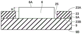
Referring to fig. 6, a semiconductor device 200 of the present embodiment has basically the same configuration as the semiconductor device 100 of embodiment 1 shown in fig. 1. Therefore, in the semiconductor device 200 of fig. 6, the same components as those of the semiconductor device 100 of fig. 1 are denoted by the same reference numerals, and the description thereof will not be repeated. The semiconductor device 200 is different from the semiconductor device 100 in that the control semiconductor element 6 is located at a different position in the vertical direction in fig. 6.
As described above, the control semiconductor element 6 has the structure including the package 61 and the lead frame 62, but here, one main surface 6A of the control semiconductor element 6 and the other main surface 6B opposite thereto are considered. One main surface 6A is the upper main surface in fig. 6 of the pair of main surfaces of the main body of the control semiconductor element 6 (e.g., the main body of the package 61), and the other main surface 6B is the lower main surface in fig. 6. Similarly, the cover 23 also has one main surface 23A on the upper side of fig. 6 and the other main surface 23B on the opposite side.
As shown by a region a surrounded by a broken line in fig. 6, in the present embodiment, the hole 25 of the cover 23 overlaps the entire control semiconductor element 6 in a plan view. And is arranged such that the control semiconductor element 6 is inserted into the hole portion 25. Referring to fig. 7, in region a in fig. 6, one main surface 23A of cover 23 on the side opposite to base plate 1 may be disposed at a position coplanar with one main surface 6A of control semiconductor element 6 on the side opposite to base plate 1. Alternatively, referring to fig. 8, in the region a of fig. 6, one main surface 23A of the cover 23 on the opposite side to the base plate 1 may be disposed on the base plate 1 side, i.e., on the lower side of fig. 6, as compared to the one main surface 6A of the control semiconductor element 6 on the opposite side to the base plate 1. In the case of fig. 8, one main surface 6A is raised upward by dimension H compared to one main surface 23A.
In this embodiment, the control semiconductor element 6 and the control circuit board 9 are disposed entirely above the semiconductor device 200, as compared with embodiment 1. Therefore, the region below the control circuit board 9, that is, the region filled with the resin material 35 is deeper in the vertical direction in fig. 6 than in embodiment 1, and substantially the entire inside of the container-like member constituted by the base plate 1 and the case 3 is covered with the resin material 35.
Next, the operation and effects of the present embodiment will be described. This embodiment achieves the following operational effects in addition to the operational effects of embodiment 1.
In embodiment 1, the uppermost surface of the lid 23 is disposed above the uppermost surface of the control semiconductor element 6, and the uppermost surface of the control semiconductor element 6 is disposed inside the container-shaped member formed by the base plate 1 and the case 3. Therefore, it is difficult to mount the cooling device on the uppermost surface of the control semiconductor element 6 on the user side. However, by disposing one main surface 23A, which is the uppermost surface of the cover 23, below one main surface 6A, which is the uppermost surface of the control semiconductor element 6 as in the present embodiment, the one main surface 6A of the control semiconductor element 6 is easily touched by the user. Therefore, it becomes easy to mount a cooling device such as a heat dissipating fin on one main surface 6A on the user side as compared with embodiment 1. By mounting this cooling device, the effect of suppressing an excessive temperature rise of the control semiconductor element 6 is improved.
Referring to fig. 9, a semiconductor device 300 according to this embodiment has basically the same configuration as the semiconductor device 100 according to embodiment 1 shown in fig. 1. Therefore, in the semiconductor device 300 of fig. 9, the same components as those of the semiconductor device 100 of fig. 1 are denoted by the same reference numerals, and the description thereof will not be repeated. The semiconductor device 300 is different from the semiconductor device 100 in that a heat sink 41 is further provided on one main surface 6A of the control semiconductor element 6 on the opposite side to the base plate 1, and the heat sink 41 is arranged to close the hole 25 of the cover 23 located directly above the control semiconductor element 6.
The heat sink 41 is preferably formed of a metal plate such as aluminum. Further, heat sink 41 is preferably in contact with main surface 6A so as to cover the entire main surface 6A of control semiconductor element 6. In fig. 9, the planar areas of the heat sink 41 and the control semiconductor element 6 are equal. However, the planar shape of the heat sink 41 is basically arbitrary, and may have a size that partially protrudes outside the control semiconductor element 6 in a plan view (that is, the heat sink 41 is larger than the control semiconductor element 6).
The heat sink 41 is disposed such that its lowermost surface is in contact with the one main surface 6A of the control semiconductor element 6, and its uppermost surface closes the end of the hole 25 closest to the base plate 1 (lower side in fig. 9), and is in contact with the other main surface 23B of the cover 23 in the region adjacent to the hole 25 in plan view. Therefore, in the semiconductor device 300, the hole 25 is disposed only in a part of the region overlapping the heat sink 41 in a plan view, and the planar area of the hole 25 is smaller than that of the heat sink 41. When the planar areas of the heat sink 41 and the control semiconductor element 6 are equal, the hole 25 may be disposed only in a part of the region overlapping the control semiconductor element 6 in a plan view, and the planar area of the hole 25 may be smaller than the control semiconductor element 6. Thereby, the heat dissipation plate 41 closes the entire hole 25, and blocks the flow of air or the like between the inside and the outside of the container-shaped member constituted by the base plate 1 and the housing 3.
Next, the operation and effects of the present embodiment will be described. This embodiment achieves the following operational effects in addition to the operational effects of embodiment 1.
In embodiment 1, by providing the hole 25 in the lid 23, the circulation of the atmosphere or the like between the inside and the outside of the container-like member constituted by the base plate 1 and the case 3 can be realized. This improves the efficiency of heat dissipation of the control semiconductor element 6 to the outside, but foreign matter mixed from the outside of the semiconductor device 100 may adhere to the one main surface 6A of the control semiconductor element 6.
Therefore, by providing the heat dissipation plate 41 that covers the one main surface 6A of the control semiconductor element 6 and closes the hole 25 of the cover 23 as in the present embodiment, it is possible to suppress adhesion of foreign matter to the one main surface 6A of the control semiconductor element 6 while ensuring heat dissipation from the control semiconductor element 6 to the outside of the semiconductor device 100.
Embodiment 4
Referring to fig. 10, a semiconductor device 400 according to this embodiment has basically the same configuration as the semiconductor device 100 according to embodiment 1 shown in fig. 1 and the semiconductor device 300 according to embodiment 3 shown in fig. 9. Therefore, in the semiconductor device 400 of fig. 10, the same components as those of the semiconductor devices 100 and 300 of fig. 1 and 9 are denoted by the same reference numerals, and the description thereof will not be repeated.
The semiconductor device 400 is different from the semiconductor device 300 in that the heat sink 41 includes: a 1 st heat-dissipating plate portion 41A housed in the hole portion 25 of the cover 23; and a portion 41B of the 2 nd heat dissipation plate extending from the portion of the 1 st heat dissipation plate 41A to the inside of the case 3, i.e., the lower side in fig. 10. The lowermost portion of the 2 nd heat sink part 41B is in contact with the upper surface of the one main surface 6A of the control semiconductor element 6, and particularly, in fig. 10, the 2 nd heat sink part 41B is in contact with the entire surface of the one main surface 6A. Therefore, the planar areas of the portion 41B of the 2 nd heat dissipation plate and the one main surface 6A are equal. The portion 41A of the 1 st heat sink is disposed so as to cover the inner wall of the hole 25 and fill the entire hole 25.
In fig. 10, the planar area of the hole portion 25 is larger than that of the control semiconductor element 6, and the hole portion 25 is arranged so as to overlap with the entire region overlapping with the control semiconductor element 6 in a plan view and also overlap with a region adjacent to the outer edge of the control semiconductor element 6. Therefore, the planar area of the 1 st heat sink 41A that is entirely filled to cover the inner wall of the hole 25 is larger than that of the 2 nd heat sink 41B that is in contact with the control semiconductor element 6. However, for example, as shown in fig. 9, in the present embodiment, the hole 25 may have a smaller planar area than the control semiconductor element 6, and the heat sink 41 may be disposed such that the heat sink 41 has a portion of the 1 st heat sink 41A filling the hole 25 and a portion of the 2 nd heat sink 41B contacting the control semiconductor element 6 therebelow.
Next, the operation and effects of the present embodiment will be described. This embodiment achieves the following operational effects in addition to the operational effects of embodiment 3.
In the structure of embodiment 3 in which the heat generated by the control semiconductor element 6 is radiated to the outside of the hole portion 25 using the heat radiation plate 41, it is more preferable to provide a cooling device such as a fan on the upper surface of the heat radiation plate 41 on the user side, for example, in order to further improve the cooling efficiency. However, in embodiment 3, since the uppermost surface of the heat sink 41 is located at a lower position than the one main surface 23A of the cover 23, it is difficult to attach a cooling device such as a heat dissipating fin to the upper surface of the heat sink 41.
Therefore, in the semiconductor device 400 of the present embodiment, the heat sink 41 has both a portion of the 1 st heat sink 41A accommodated in the hole 25 and a portion of the 2 nd heat sink 41B contacting the control semiconductor element 6 on the lower side thereof. In this way, the uppermost surface of the heat sink 41 is disposed at a higher position than in embodiment 3. Therefore, the heat dissipation effect of the heat dissipation plate 41 itself to the heat generated by the control semiconductor element 6 can be ensured, and the cooling device such as the heat dissipation fin can be easily mounted on the upper surface of the heat dissipation plate 41.
In fig. 10, the uppermost surface of the 1 st heat sink 41A of the heat sink 41 is disposed at a position coplanar with the one main surface 23A of the cover 23, but the uppermost surface of the 1 st heat sink 41A may be raised above the one main surface 23A, in other words, to the outside of the semiconductor device 100. Even in this case, the cooling device can be easily mounted on the heat sink 41, and the heat sink 41 is exposed to the outside of the semiconductor device 100, so that the heat dissipation to the control semiconductor element 6 can be further improved.
Referring to fig. 11, a semiconductor device 500 of the present embodiment has basically the same configuration as the semiconductor device 200 of embodiment 2 shown in fig. 6. Therefore, in the semiconductor device 500 of fig. 11, the same components as those of the semiconductor device 200 of fig. 6 are denoted by the same reference numerals, and the description thereof will not be repeated. The semiconductor device 500 is different from the semiconductor device 200 in that it further includes a peltier element 71 above the one main surface 23A of the cover 23 on the side opposite to the base plate 1.
The peltier element 71 is disposed such that, in fig. 11, the lowermost surface thereof is in contact with one main surface 23A of the cover 23 and one main surface 6A of the control semiconductor element 6. However, the present invention is not limited to the above-described embodiment, and for example, as in the case where the peltier element 71 is applied to the configuration shown in fig. 8 of embodiment 2, the lowermost surface of the peltier element 71 may be in contact with the one main surface 6A, but may be in contact with the one main surface 23A, but may be in a state of floating upward with respect to the one main surface 23A. When the peltier element 71 is applied to the semiconductor device 400 of fig. 10 of embodiment 4, the uppermost surface of the heat sink 41 and the one main surface 23A of the cover 23 are in contact with the lowermost surface of the peltier element 71, but such a configuration is also possible.
As the power source of the peltier element 71, a power source for a control circuit of the smart power module, that is, a power source for driving the control semiconductor element 6 mounted on the control circuit board 9 is used. This eliminates the need to additionally provide a power supply for the peltier element 71.
Referring to fig. 12, the peltier element 71 in the region XII surrounded by the dotted line in fig. 11 is composed of a plurality of thermoelectric elements 72, a plurality of electrodes 73, and 1 pair of ceramic substrates 74. The plurality of thermoelectric elements 72 are formed of a combination of a p-type semiconductor and an n-type semiconductor of silicon, for example. Here, for example, in the left-right direction of fig. 12, the p-type semiconductor and the n-type semiconductor are alternately arranged.
The plurality of electrodes 73 are formed of a metal material such as copper. The plurality of electrodes 73 are connected to both of 1 pair of thermoelectric elements 72 adjacent to each other in the left-right direction of fig. 12, and the electrodes 73 are alternately arranged between the upper region and the lower region of the thermoelectric element 72 in fig. 12. That is, for example, if the 1 st thermoelectric element 72 and the 2 nd thermoelectric element 72 adjacent thereto are connected by the electrode 73 on their upper sides, the 2 nd thermoelectric element 72 and the 3 rd thermoelectric element 72 adjacent to the 2 nd thermoelectric element 72 on the opposite side of the 1 st thermoelectric element 72 are connected by the electrode 73 on their lower sides.
In the above manner, all the thermoelectric elements 72 and the electrodes 73 are integrally connected. The pair of ceramic substrates 74 1 were arranged so that all of the integrated thermoelectric elements 72 and electrodes 73 were sandwiched from above and below.
Next, the operation and effects of the present embodiment will be described. The present embodiment achieves the following operational effects in addition to the operational effects of the above-described embodiments.
In the semiconductor devices according to the above embodiments, a cooling device needs to be provided on the user side in order to further improve the cooling effect. However, in the present embodiment, the peltier element 71 is provided above the one main surface 23A of the cover 23. This enables the control semiconductor element 6 to be efficiently cooled via the peltier element without providing the cooling device.
As described above, the control semiconductor element 6 used in each embodiment includes the package 61 and the lead frame 62 (see fig. 3). Referring to fig. 13, in the present embodiment, a plurality of recesses 63 having a depth of 500 μm or more are included in at least a part of the surface of the package 61. The plurality of recesses 63, i.e., 2 or more, are formed on the surface of the package 61 with a space therebetween. The depth of the recess 63, i.e., the vertical dimension in fig. 13, is greater than or equal to 500 μm on the surface of the package 61 than the region other than the region where the recess 63 is formed. More preferably, the depth of the recess 63 is 600 μm or more.
As shown in fig. 13, 2 or more recesses 63 may be formed on both the uppermost surface of the package 61, i.e., the surface on the side opposite to the base plate 1 during mounting, and the lowermost surface of the package 61, i.e., the surface on the base plate 1 during mounting. However, 2 or more recesses 63 may be formed only in one of the uppermost surface and the lowermost surface of the package.
The control semiconductor element 6 having the surface features of the package 61 can be applied to the semiconductor devices 100 to 500 of any of the above embodiments. The semiconductor device of the present embodiment basically has the same structure as the semiconductor devices 100 to 500 of embodiments 1 to 5 except for the surface of the package 61, and therefore, description of the structural features thereof is omitted.
Next, the operation and effects of the present embodiment will be described. This embodiment achieves the following operational effects in addition to the operational effects of embodiments 1 to 5 described above.
As described above, by providing the recessed portion 63 having a depth of 500 μm or more on the surface of the package 61 included in the control semiconductor element 6, the surface area of the package 61 is increased as compared with the case where the recessed portion 63 is not formed. Therefore, heat dissipation from the surface of the control semiconductor element 6 can be improved.
Embodiment 7
Referring to fig. 14, in the semiconductor device 600 of the present embodiment, a high heat-dissipating resin 36 is disposed in place of the resin material 35 in an area inside the container-like member including the base plate 1 and the case 3, particularly below the control circuit board 9. The high heat-dissipating resin 36 is disposed so as to cover the surfaces of the power semiconductor substrate 8 and the power semiconductor element 5, the other main surface 9B of the control circuit substrate 9, a part of the inner surface of the case wall portion 3A, a part of the surface of the main electrode terminal 15, and the like, as in the case of the resin material 35 of fig. 1 and the like. As described above, the high heat-dissipating resin 36 is filled in the case 3 so as to encapsulate the power semiconductor element 5.
The high heat dissipation resin 36 is made of a resin such as silicone gel or epoxy resin, similarly to the resin material 35. However, the high heat-dissipating resin 36 has higher heat dissipation than the resin material 35. Specifically, the thermal conductivity of the high heat dissipating resin 36 is 0.5W/(m.K) or more. More preferably, the thermal conductivity is 0.6W/(mK) or more.
Fig. 14 shows an example in which the high heat-dissipating resin 36 is applied to the semiconductor device 200 of embodiment 2 as an example. However, the present invention is not limited to this, and the high heat dissipation resin 36 may be applied to any of the semiconductor devices 100 to 500 according to the above embodiments. The semiconductor device of the present embodiment basically has the same structure as the semiconductor devices 100 to 500 of the above embodiments except for the surface of the package 61, and therefore, description of the structural features thereof is omitted.
Next, the operation and effects of the present embodiment will be described. This embodiment achieves the following operational effects in addition to the operational effects of embodiments 1 to 6 described above.
In each of embodiments 1 to 6, there is a possibility that a heat dissipation method of heat transferred from the control semiconductor element 6 and the control circuit board 9 to the resin material 35 may become a problem. However, in the present embodiment, the heat transferred from the control semiconductor element 6 and the control circuit board 9 to the heat-dissipating resin 36 can be efficiently dissipated from the base plate 1 side to the outside of the semiconductor device 600, for example. Therefore, the heat dissipation of the control semiconductor element 6 can be further improved as compared with the embodiments 1 to 6.
The features described in the above embodiments (including the examples) can be combined as appropriate in a range not technically contradictory.
While the embodiments of the present invention have been described, the embodiments disclosed herein are illustrative in all respects and are not intended to be limiting. The scope of the present invention is indicated by the claims, and all changes that come within the meaning and range of equivalency of the claims are intended to be embraced therein.
Claims (4)
1. A semiconductor device, comprising:
a base plate;
a housing disposed above the base plate;
a power semiconductor element disposed on the base plate in the case; and
a control semiconductor element disposed inside the case,
an opening is formed in the case on the side opposite to the base plate,
the semiconductor device further includes a cover for closing the opening of the case,
a hole is formed in at least a part of a region of the lid that overlaps with the control semiconductor element in a plan view,
the hole portion overlaps with the entire control semiconductor element in a plan view,
the control semiconductor element is disposed in the hole,
the main surface of the lid on the side opposite to the base plate is disposed at a position coplanar with the main surface of the control semiconductor element on the side opposite to the base plate, or at a position closer to the base plate side than the main surface of the control semiconductor element on the side opposite to the base plate.
2. The semiconductor device according to claim 1,
the cover further has a peltier element above a main surface of the cover on the opposite side of the base plate.
3. The semiconductor device according to claim 1,
the control semiconductor element includes a package member,
the package includes a plurality of recesses having a depth of 500 [ mu ] m or more in at least a part of a surface of the package.
4. The semiconductor device according to claim 1,
the case further contains a high heat-dissipating resin filled to encapsulate the power semiconductor element, and the high heat-dissipating resin has a thermal conductivity of 0.5W/(m.K) or more.
Applications Claiming Priority (2)
| Application Number | Priority Date | Filing Date | Title |
|---|---|---|---|
| JP2016083444A JP6552450B2 (en) | 2016-04-19 | 2016-04-19 | Semiconductor device |
| JP2016-083444 | 2016-04-19 |
Publications (2)
| Publication Number | Publication Date |
|---|---|
| CN107452688A CN107452688A (en) | 2017-12-08 |
| CN107452688B true CN107452688B (en) | 2020-09-25 |
Family
ID=59980925
Family Applications (1)
| Application Number | Title | Priority Date | Filing Date |
|---|---|---|---|
| CN201710258116.9A Active CN107452688B (en) | 2016-04-19 | 2017-04-19 | Semiconductor device with a plurality of semiconductor chips |
Country Status (4)
| Country | Link |
|---|---|
| US (1) | US10062632B2 (en) |
| JP (1) | JP6552450B2 (en) |
| CN (1) | CN107452688B (en) |
| DE (1) | DE102017206195B4 (en) |
Families Citing this family (3)
| Publication number | Priority date | Publication date | Assignee | Title |
|---|---|---|---|---|
| JP7038645B2 (en) * | 2018-12-06 | 2022-03-18 | 三菱電機株式会社 | Semiconductor devices and methods for manufacturing semiconductor devices |
| CN112467957A (en) * | 2020-10-10 | 2021-03-09 | 山东斯力微电子有限公司 | Intelligent high-power IGBT module |
| CN112864112A (en) * | 2021-01-19 | 2021-05-28 | 安徽安晶半导体有限公司 | Insulating high-power semiconductor module |
Citations (1)
| Publication number | Priority date | Publication date | Assignee | Title |
|---|---|---|---|---|
| JPH10229146A (en) * | 1997-02-17 | 1998-08-25 | Seiko Epson Corp | Semiconductor device |
Family Cites Families (15)
| Publication number | Priority date | Publication date | Assignee | Title |
|---|---|---|---|---|
| JPS51160119U (en) * | 1975-06-14 | 1976-12-20 | ||
| JPS583784U (en) * | 1981-07-01 | 1983-01-11 | 株式会社日立ホームテック | automotive converter |
| US5285107A (en) * | 1989-04-20 | 1994-02-08 | Sanyo Electric Co., Ltd. | Hybrid integrated circuit device |
| JPH04138693A (en) * | 1990-09-29 | 1992-05-13 | Toshiba Lighting & Technol Corp | Lighting device for discharge lamp |
| JPH09211266A (en) * | 1996-01-30 | 1997-08-15 | Hitachi Ltd | Semiconductor device and optical communication module |
| US6094919A (en) * | 1999-01-04 | 2000-08-01 | Intel Corporation | Package with integrated thermoelectric module for cooling of integrated circuits |
| JP4044265B2 (en) * | 2000-05-16 | 2008-02-06 | 三菱電機株式会社 | Power module |
| JP3764687B2 (en) * | 2002-02-18 | 2006-04-12 | 三菱電機株式会社 | Power semiconductor device and manufacturing method thereof |
| US6999317B2 (en) * | 2003-08-12 | 2006-02-14 | Delphi Technologies, Inc. | Thermally enhanced electronic module with self-aligning heat sink |
| JP2006121861A (en) | 2004-10-25 | 2006-05-11 | Fuji Electric Fa Components & Systems Co Ltd | Power converter |
| US20080178920A1 (en) * | 2006-12-28 | 2008-07-31 | Schlumberger Technology Corporation | Devices for cooling and power |
| CN101214918B (en) * | 2007-01-04 | 2012-04-18 | 菱生精密工业股份有限公司 | Packaging structure used for micro-electromechanical capping process |
| US9052724B2 (en) * | 2012-08-07 | 2015-06-09 | International Business Machines Corporation | Electro-rheological micro-channel anisotropic cooled integrated circuits and methods thereof |
| JP6119313B2 (en) * | 2013-03-08 | 2017-04-26 | 富士電機株式会社 | Semiconductor device |
| JP6120704B2 (en) * | 2013-07-03 | 2017-04-26 | 三菱電機株式会社 | Semiconductor device |
-
2016
- 2016-04-19 JP JP2016083444A patent/JP6552450B2/en active Active
- 2016-12-21 US US15/386,764 patent/US10062632B2/en active Active
-
2017
- 2017-04-11 DE DE102017206195.2A patent/DE102017206195B4/en active Active
- 2017-04-19 CN CN201710258116.9A patent/CN107452688B/en active Active
Patent Citations (1)
| Publication number | Priority date | Publication date | Assignee | Title |
|---|---|---|---|---|
| JPH10229146A (en) * | 1997-02-17 | 1998-08-25 | Seiko Epson Corp | Semiconductor device |
Also Published As
| Publication number | Publication date |
|---|---|
| US20170301603A1 (en) | 2017-10-19 |
| JP2017195677A (en) | 2017-10-26 |
| DE102017206195A1 (en) | 2017-10-19 |
| CN107452688A (en) | 2017-12-08 |
| JP6552450B2 (en) | 2019-07-31 |
| DE102017206195B4 (en) | 2020-11-26 |
| US10062632B2 (en) | 2018-08-28 |
Similar Documents
| Publication | Publication Date | Title |
|---|---|---|
| JP3804861B2 (en) | Electrical device and wiring board | |
| US8373197B2 (en) | Circuit device | |
| CN109637983B (en) | Chip package | |
| CN111261598B (en) | Packaging structure and power module applicable to same | |
| JP7107295B2 (en) | electronic device | |
| CN107452688B (en) | Semiconductor device with a plurality of semiconductor chips | |
| JP7247574B2 (en) | semiconductor equipment | |
| US10163752B2 (en) | Semiconductor device | |
| US11195775B2 (en) | Semiconductor module, semiconductor device, and manufacturing method of semiconductor module | |
| US11239131B2 (en) | Semiconductor module | |
| JP4375299B2 (en) | Power semiconductor device | |
| TWI660471B (en) | Chip package | |
| KR102313764B1 (en) | Cooling system for semiconductor component having semiconductor chip with cooling apparatus | |
| JP7392319B2 (en) | semiconductor equipment | |
| JP3855726B2 (en) | Power module | |
| JPH02278856A (en) | Semiconductor integrated circuit device | |
| JPH11220074A (en) | Semiconductor device | |
| US20230253291A1 (en) | Power semiconductor module arrangement and methods for producing a semiconductor arrangement | |
| JP2006041199A (en) | Electronic device | |
| JP2017005129A (en) | Semiconductor device | |
| KR20160009950A (en) | Leadframe and power semicondductor package | |
| JPH1044657A (en) | Card type electronic device | |
| JP2005203570A (en) | Semiconductor module | |
| JPH05129483A (en) | Hybrid ic | |
| JPH1117084A (en) | Power semiconductor device and power controller using the same |
Legal Events
| Date | Code | Title | Description |
|---|---|---|---|
| PB01 | Publication | ||
| PB01 | Publication | ||
| SE01 | Entry into force of request for substantive examination | ||
| SE01 | Entry into force of request for substantive examination | ||
| GR01 | Patent grant | ||
| GR01 | Patent grant |