CN107039387B - Lead frame, semiconductor device, and method for manufacturing lead frame - Google Patents
Lead frame, semiconductor device, and method for manufacturing lead frame Download PDFInfo
- Publication number
- CN107039387B CN107039387B CN201710012575.9A CN201710012575A CN107039387B CN 107039387 B CN107039387 B CN 107039387B CN 201710012575 A CN201710012575 A CN 201710012575A CN 107039387 B CN107039387 B CN 107039387B
- Authority
- CN
- China
- Prior art keywords
- lead
- frame
- lead frame
- resin
- leads
- Prior art date
- Legal status (The legal status is an assumption and is not a legal conclusion. Google has not performed a legal analysis and makes no representation as to the accuracy of the status listed.)
- Active
Links
Images


Classifications
-
- H—ELECTRICITY
- H01—ELECTRIC ELEMENTS
- H01L—SEMICONDUCTOR DEVICES NOT COVERED BY CLASS H10
- H01L23/00—Details of semiconductor or other solid state devices
- H01L23/48—Arrangements for conducting electric current to or from the solid state body in operation, e.g. leads, terminal arrangements ; Selection of materials therefor
- H01L23/488—Arrangements for conducting electric current to or from the solid state body in operation, e.g. leads, terminal arrangements ; Selection of materials therefor consisting of soldered or bonded constructions
- H01L23/495—Lead-frames or other flat leads
- H01L23/49537—Plurality of lead frames mounted in one device
-
- H—ELECTRICITY
- H01—ELECTRIC ELEMENTS
- H01L—SEMICONDUCTOR DEVICES NOT COVERED BY CLASS H10
- H01L21/00—Processes or apparatus adapted for the manufacture or treatment of semiconductor or solid state devices or of parts thereof
- H01L21/02—Manufacture or treatment of semiconductor devices or of parts thereof
- H01L21/04—Manufacture or treatment of semiconductor devices or of parts thereof the devices having at least one potential-jump barrier or surface barrier, e.g. PN junction, depletion layer or carrier concentration layer
- H01L21/48—Manufacture or treatment of parts, e.g. containers, prior to assembly of the devices, using processes not provided for in a single one of the subgroups H01L21/06 - H01L21/326
- H01L21/4814—Conductive parts
- H01L21/4821—Flat leads, e.g. lead frames with or without insulating supports
-
- H—ELECTRICITY
- H01—ELECTRIC ELEMENTS
- H01L—SEMICONDUCTOR DEVICES NOT COVERED BY CLASS H10
- H01L23/00—Details of semiconductor or other solid state devices
- H01L23/28—Encapsulations, e.g. encapsulating layers, coatings, e.g. for protection
- H01L23/29—Encapsulations, e.g. encapsulating layers, coatings, e.g. for protection characterised by the material, e.g. carbon
- H01L23/293—Organic, e.g. plastic
-
- H—ELECTRICITY
- H01—ELECTRIC ELEMENTS
- H01L—SEMICONDUCTOR DEVICES NOT COVERED BY CLASS H10
- H01L23/00—Details of semiconductor or other solid state devices
- H01L23/28—Encapsulations, e.g. encapsulating layers, coatings, e.g. for protection
- H01L23/31—Encapsulations, e.g. encapsulating layers, coatings, e.g. for protection characterised by the arrangement or shape
- H01L23/3107—Encapsulations, e.g. encapsulating layers, coatings, e.g. for protection characterised by the arrangement or shape the device being completely enclosed
- H01L23/3142—Sealing arrangements between parts, e.g. adhesion promotors
-
- H—ELECTRICITY
- H01—ELECTRIC ELEMENTS
- H01L—SEMICONDUCTOR DEVICES NOT COVERED BY CLASS H10
- H01L23/00—Details of semiconductor or other solid state devices
- H01L23/48—Arrangements for conducting electric current to or from the solid state body in operation, e.g. leads, terminal arrangements ; Selection of materials therefor
- H01L23/488—Arrangements for conducting electric current to or from the solid state body in operation, e.g. leads, terminal arrangements ; Selection of materials therefor consisting of soldered or bonded constructions
- H01L23/495—Lead-frames or other flat leads
- H01L23/49541—Geometry of the lead-frame
- H01L23/49548—Cross section geometry
-
- H—ELECTRICITY
- H01—ELECTRIC ELEMENTS
- H01L—SEMICONDUCTOR DEVICES NOT COVERED BY CLASS H10
- H01L23/00—Details of semiconductor or other solid state devices
- H01L23/48—Arrangements for conducting electric current to or from the solid state body in operation, e.g. leads, terminal arrangements ; Selection of materials therefor
- H01L23/488—Arrangements for conducting electric current to or from the solid state body in operation, e.g. leads, terminal arrangements ; Selection of materials therefor consisting of soldered or bonded constructions
- H01L23/495—Lead-frames or other flat leads
- H01L23/49541—Geometry of the lead-frame
- H01L23/49558—Insulating layers on lead frames, e.g. bridging members
-
- H—ELECTRICITY
- H01—ELECTRIC ELEMENTS
- H01L—SEMICONDUCTOR DEVICES NOT COVERED BY CLASS H10
- H01L23/00—Details of semiconductor or other solid state devices
- H01L23/48—Arrangements for conducting electric current to or from the solid state body in operation, e.g. leads, terminal arrangements ; Selection of materials therefor
- H01L23/488—Arrangements for conducting electric current to or from the solid state body in operation, e.g. leads, terminal arrangements ; Selection of materials therefor consisting of soldered or bonded constructions
- H01L23/495—Lead-frames or other flat leads
- H01L23/49589—Capacitor integral with or on the leadframe
-
- H—ELECTRICITY
- H01—ELECTRIC ELEMENTS
- H01L—SEMICONDUCTOR DEVICES NOT COVERED BY CLASS H10
- H01L23/00—Details of semiconductor or other solid state devices
- H01L23/48—Arrangements for conducting electric current to or from the solid state body in operation, e.g. leads, terminal arrangements ; Selection of materials therefor
- H01L23/488—Arrangements for conducting electric current to or from the solid state body in operation, e.g. leads, terminal arrangements ; Selection of materials therefor consisting of soldered or bonded constructions
- H01L23/498—Leads, i.e. metallisations or lead-frames on insulating substrates, e.g. chip carriers
- H01L23/49861—Lead-frames fixed on or encapsulated in insulating substrates
-
- H—ELECTRICITY
- H01—ELECTRIC ELEMENTS
- H01L—SEMICONDUCTOR DEVICES NOT COVERED BY CLASS H10
- H01L2224/00—Indexing scheme for arrangements for connecting or disconnecting semiconductor or solid-state bodies and methods related thereto as covered by H01L24/00
- H01L2224/01—Means for bonding being attached to, or being formed on, the surface to be connected, e.g. chip-to-package, die-attach, "first-level" interconnects; Manufacturing methods related thereto
- H01L2224/42—Wire connectors; Manufacturing methods related thereto
- H01L2224/47—Structure, shape, material or disposition of the wire connectors after the connecting process
- H01L2224/48—Structure, shape, material or disposition of the wire connectors after the connecting process of an individual wire connector
- H01L2224/4805—Shape
- H01L2224/4809—Loop shape
- H01L2224/48091—Arched
-
- H—ELECTRICITY
- H01—ELECTRIC ELEMENTS
- H01L—SEMICONDUCTOR DEVICES NOT COVERED BY CLASS H10
- H01L2924/00—Indexing scheme for arrangements or methods for connecting or disconnecting semiconductor or solid-state bodies as covered by H01L24/00
- H01L2924/15—Details of package parts other than the semiconductor or other solid state devices to be connected
- H01L2924/181—Encapsulation
Abstract
The invention provides a lead frame, a semiconductor device and a method for manufacturing the lead frame. A leadframe, comprising: a first lead frame including a first lead; a second lead frame including a second lead bonded to the first lead; and a resin portion provided between the first lead frame and the second lead frame, wherein the first lead and the second lead each include an embedded portion embedded in the resin portion and a protruding portion protruding from the resin portion, and the embedded portion of the first lead and the embedded portion of the second lead are joined in the resin portion.
Description
Technical Field
The present invention relates to a lead frame and a semiconductor device.
Background
Conventionally, a leadless semiconductor device such as QFN (Quad Flat No Lead) is known as a semiconductor device including a Lead frame. In the semiconductor device, recently, it is necessary to increase the number of terminals and to provide the terminals in a plurality of columns or the like in correspondence with the number.
However, in order to provide the terminals in a plurality of columns, it is necessary to provide wirings having a narrow pitch. The wiring of the lead frame is formed by etching and penetrating the upper and lower surfaces of the metal plate. Since etching is performed not only in the depth direction but also in the width direction, if the metal plate is thick, the space between the wirings becomes wide, and the wirings cannot be provided with a narrow pitch. Therefore, a metal plate having a thickness of about 0.2mm has been conventionally used. However, in order to provide wirings with a narrower pitch, the use of a thinner metal plate has been studied.
However, if the wiring is formed by etching a thin metal plate, the possibility of deformation of the wiring increases. Therefore, it is difficult to realize a lead frame using a metal plate thinner than a certain degree or more.
< Prior Art document >
< patent document >
Patent document 1: japanese patent laid-open publication No. 2000-307049
Disclosure of Invention
< problems to be solved by the present invention >
In view of the above problems, an object of the present invention is to provide a lead frame that is less likely to deform even when made thin.
< solution to problem >
According to one embodiment, there is provided a lead frame, including: a first lead frame including a first lead; a second lead frame including a second lead bonded to the first lead; and a resin portion provided between the first lead frame and the second lead frame, wherein the first lead and the second lead each include an embedded portion embedded in the resin portion and a protruding portion protruding from the resin portion, and the embedded portion of the first lead and the embedded portion of the second lead are joined in the resin portion.
Drawings
Other objects, features and advantages of the present invention will become more apparent when the following detailed description is read with reference to the accompanying drawings.
Fig. 1 is a plan view showing an example of a lead frame according to the first embodiment.
Fig. 2A to 2D are diagrams showing examples of unit lead frames constituting the lead frame of the first embodiment.
Fig. 3A to 3C are diagrams (1) showing an example of manufacturing steps of the lead frame according to the first embodiment.
Fig. 4A to 4C are diagrams (fig. 2) showing an example of manufacturing steps of the lead frame according to the first embodiment.
Fig. 5A to 5D are diagrams (fig. 3) showing an example of manufacturing steps of the lead frame according to the first embodiment.
Fig. 6 is a cross-sectional view showing an example of a semiconductor device including the lead frame of the first embodiment.
Fig. 7 is a cross-sectional view showing modification 1 of the lead frame according to the first embodiment.
Fig. 8A to 8D are diagrams showing an example of a manufacturing process of modification 1 of the lead frame according to the first embodiment.
Fig. 9 is a cross-sectional view showing modification 2 of the lead frame according to the first embodiment.
Fig. 10A to 10D are diagrams showing an example of a manufacturing process of modification 2 of the lead frame according to the first embodiment.
Fig. 11 is a cross-sectional view showing modification 3 of the lead frame according to the first embodiment.
Fig. 12A to 12C are diagrams showing an example of a manufacturing process of modification 3 of the lead frame according to the first embodiment.
Fig. 13 is a cross-sectional view showing modification 4 of the lead frame according to the first embodiment.
Fig. 14A to 14D are diagrams (1) showing an example of a manufacturing process of modification 4 of the lead frame according to the first embodiment.
Fig. 15A to 15C are diagrams (fig. 2) showing an example of a manufacturing process of modification 4 of the lead frame according to the first embodiment.
Fig. 16 is a cross-sectional view showing an example of a unit lead frame constituting modification 5 of the lead frame of the first embodiment.
Fig. 17 is a cross-sectional view showing an example of a semiconductor device according to modification 5 in which the lead frame according to the first embodiment is used.
Fig. 18 is an enlarged view of a portion surrounded by a broken line in fig. 2C.
Description of the symbols
1 lead frame
5. 6 semiconductor device
10 base plate frame
10x, 34z slit
20 unit lead frame group
30. 30A, 30B, 30C, 30D, 30E unit lead frame
31. 32, 33, 34 frame
31y, 31z, 32y, 32z, 33y
32t, 32x opening
39 resin part
39a lower surface of the resin portion
39b upper surface of resin part
40 electronic component
45 joint part
51. 61 semiconductor chip
52 metal wiring
53. 63 sealing resin
62 bump
310. 320, 330, 340 metal plate
310a, 320a metal plate
310b, 320b metal plate lower surface
311 chip mounting part
311e buried portion
311p projection
312. 322, 332 lead wire
312e, 322e embedded part
312p, 322p protrusions
315. 315A, 315B, 315D external connection terminal
321 bonding pad
323. 343 wiring
344 cushion
Detailed Description
The invention is described below with reference to exemplary embodiments. Those skilled in the art will appreciate that various modifications can be made using the teachings of the present invention and that the invention is not limited to the embodiments shown for illustration.
(embodiment 1)
(Structure of lead frame)
Fig. 1 is a plan view showing an example of a lead frame 1 according to the first embodiment. As shown in fig. 1, the lead frame 1 includes a substrate frame 10 having a substantially rectangular shape in a plan view, and a plurality of unit lead frame groups 20 are arranged in the substrate frame 10 with a space therebetween. The unit lead frame group 20 is a group of a plurality of unit lead frames 30 arranged in a matrix.
In the example of fig. 1, three unit lead frame groups 20 are arranged in a row. However, the number of the arranged unit lead frame groups 20 may be arbitrarily determined. In addition, the unit lead frame groups 20 may be arranged in a plurality of rows. Further, although the slit 10x is provided between each adjacent unit lead frame group 20 in fig. 1, the slit 10x is not necessarily provided.
As the material of the lead frame 1, for example, copper (Cu), Cu-based alloy, iron-nickel (Fe-Ni), Fe-Ni-based alloy, or the like can be used. The thickness of the lead frame 1 may be, for example, about 0.2 mm.
The unit lead frame 30 is a semiconductor chip mounting region on which a semiconductor chip is mounted. Further, the unit lead frames 30 are finally cut into individual semiconductor devices. For the example shown in fig. 1, each unit lead frame group 20 is constituted by unit lead frames 30 arranged in 6 rows and 6 columns. However, the number of the unit lead frames 30 constituting each unit lead frame group 20 may be arbitrarily determined.
Fig. 2A to 2D are diagrams showing an example of the unit lead frame 30 constituting the lead frame 1 according to the first embodiment. Fig. 2A is a plan view, fig. 2B is a bottom view, fig. 2C is a sectional view taken along line a-a of fig. 2A and 2B, and fig. 2D is a sectional view taken along line B-B of fig. 2A and 2B. Fig. 18 is an enlarged view of a portion surrounded by a broken line in fig. 2C.
As shown in fig. 2A to 2D, the unit lead frame 30 includes a frame 31, a frame 32, and a resin portion 39. In the present embodiment, the frame 31 is a typical example of the first lead frame of the present invention. The frame 32 is a typical example of the second lead frame of the present invention.
In the present embodiment, the frame 32 side of the unit lead frame 30 is referred to as an upper side or one side, and the frame 31 side of the unit lead frame 30 is referred to as a lower side or the other side. Further, the surface on the frame 32 side of each member is referred to as one surface or an upper surface, and the surface on the frame 31 side of each member is referred to as the other surface or a lower surface. However, the unit lead frames 30 may be used in opposite directions or may be used at any angle. In the present embodiment, the term "plan view" refers to a view of an object in a direction perpendicular to one surface of the frame 32, and the term "planar shape" refers to a shape of the object viewed in a direction perpendicular to one surface of the frame 32.
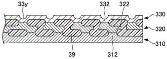
The unit lead frame 30 has a structure in which the lower surface of the frame 32 and the upper surface of the frame 31 overlap and are joined to each other by welding. The resin portion 39 is filled in a space formed between the upper surface of the frame 31 and the lower surface of the frame 32. The resin portion 39 is formed to extend in the horizontal direction from a space formed by the upper surface of the frame 31 and the lower surface of the frame 32 to a region not overlapping with the frame 31 and the frame 32 in a plan view, and forms an outer edge of a rectangular shape. The thickness of the unit lead frame 30 (thickness at the thickest portion) may be, for example, about 0.2 mm. The respective parts of the unit lead frame 30 will be described in detail hereinafter.
The frame 31 includes a chip mounting portion 311 (die pad) and a plurality of leads 312. The thickness of the frame 31 (thickness at the thickest portion) may be, for example, about 0.1 mm. The lead line 312 is a typical example of the first lead line.
The chip mounting portion 311 is mounted with a semiconductor chip. The chip mounting portion 311 may be provided at, for example, a substantially central portion of the frame 31. The chip-mounting portion 311 includes a buried portion 311e (see fig. 18) buried in the resin portion 39 and a protruding portion 311p (see fig. 18) protruding from the lower surface 39a of the resin portion 39. The thickness of the chip mounting portion 311 may be, for example, about 0.1 mm. The chip mounting portion 311 is electrically insulated from the respective leads 312.
Here, the "portion embedded in the resin portion 39" means a portion existing in a range where the resin portion 39 is provided in the thickness direction. The same applies to the other components.
The lead lines 312 may be arranged in a plurality of columns surrounding the chip mounting portion 311, for example. The lead 312 includes a buried portion 312e (see fig. 18) buried in the resin portion 39 and a protruding portion 312p (see fig. 18) protruding from the lower surface 39a of the resin portion 39. The thickness of the lead 312 is, for example, about 0.1 mm. The planar shape of the lead 312 may be, for example, a circle having a diameter of about 0.2 mm.
The frame 32 includes a plurality of bonding pads 321, a plurality of leads 322, and a plurality of wires 323. The frame 32 is provided with an opening 32x in a substantially central portion thereof for exposing the upper surface of the chip mounting portion 311 of the frame 31. The thickness of the frame 32 (thickness at the thickest portion) is, for example, about 0.1 mm. The lead wire 322 is a typical example of the second lead wire of the present invention.
The bonding pads 321 are connected to electrodes of the semiconductor chip mounted on the chip mounting portion 311 of the frame 31 via metal wires. The bonding pads 321 may be provided, for example, so as to surround the opening portion 32x (the chip mounting portion 311 of the frame 31). The bonding pads 321 may be arranged in a plurality of columns. The bonding pad 321 is provided on the upper surface 39b of the resin portion 39 and does not include a portion buried in the resin portion 39. The thickness of the bonding pad 321 may be half of the thickness of the frame 32 (thickness at the thickest portion), and may be about 0.05mm, for example.
The lead wires 322 are disposed to overlap the lead wires 312 of the frame 31, respectively, in a plan view. The lead wire 322 includes a buried portion 322e (see fig. 18) buried in the resin portion 39 and a protruding portion 322p protruding from the upper surface 39b of the resin portion 39. The embedded portions 322e of the leads 322 and the embedded portions 312e of the respective leads 312 are joined in the resin portion 39 by soldering, and the external connection terminals 315 are formed. The thickness of the lead 322 may be about 0.1 mm. The planar shape of the lead wire 322 may be a circle having a diameter of about 0.2 mm.
A recess 32y is formed in the upper surface of the lead 322. More specifically, the concave portion 32y is provided at the protruding portion 322p formed directly above the buried portion 322e of the lead 322. The recess 32y is provided as a mark for welding, and the thickness of the frame 32 can be locally reduced by providing the recess 32y, so that welding efficiency can be improved. In the present embodiment, since the lead 312 and the lead 322 are mainly joined by welding, the concave portion 32y is provided on the upper surface of the lead 322. However, portions other than the lead 312 and the lead 322 may be joined by welding. For example, in the present embodiment, the concave portion 32y is also provided at a plurality of positions (8 positions in the example shown in fig. 2A to 2D) of the frame 32 inside the bonding pad 321. Thereafter, the frame 31 is joined to the frame 32 by welding thereto. The frame 31 and the frame 32 may be welded at an arbitrarily selected portion other than that shown here in consideration of the required joint strength and the like. At this time, the concave portion 32y may be provided at the arbitrarily selected portions.
A recess 32z is formed in the lower surface of the frame 32. The depth of the recess 32z is about half of the thickness of the frame 32 (thickness at the thickest portion), and may be about 0.05mm, for example. Further, a recess 31z is formed in the upper surface of the frame 31. The depth of the recess 31z is about half of the thickness of the frame 31 (thickness at the thickest portion), and may be about 0.05mm, for example. The resin portion 39 is filled in a space formed by the concave portion 32z of the frame 32 and the concave portion 31z of the frame 31, and extends to the outside of the space. As the material of the resin portion 39, for example, a thermosetting epoxy resin or the like can be used. The thickness of the resin portion 39 may be, for example, about 0.1 mm.
A constricted portion is formed on the side of the buried portion 322e of the lead 322 by the corresponding recessed portion 32z, and a constricted portion is formed on the side of the buried portion 312e of the lead 312 by the corresponding recessed portion 31 z. The resin portion 39 is filled in the constricted portion on the side surface of the embedded portion 322e of the lead 322 and the constricted portion on the side surface of the embedded portion 312e of the lead 312. Thereby, an anchor portion (anchor) is formed for each external connection terminal 315, preventing the external connection terminal 315 from being pulled out from the resin portion 39. Similarly, an anchor portion is formed on a side surface of the chip mounting portion 311 to prevent the chip mounting portion 311 from being pulled out of the resin portion 39.
It is preferable to perform surface roughening treatment or oxidation treatment on the portions of lead wires 312 and 322 that are in contact with the surface of resin portion 39 in order to improve the adhesion of lead wires 312 and 322 to resin portion 39.
Wiring 323 may be provided in an arbitrarily selected region of upper surface 39b of resin portion 39, where bonding pad 321 and lead 322 are not provided. The wiring 323 does not include a portion embedded in the resin portion 39. The wiring 323 can be electrically connected to the bonding pad 321 and the lead 322, respectively, as appropriate. The thickness of the wiring 323 may be about half of the thickness of the frame 32 (thickness at the thickest portion), and may be 0.05mm, for example. The line/space (line/space) of the wiring 323 may be, for example, about 30 μm/60 μm.
Here, the line of the line/space represents a wiring width, and the space of the line/space represents a space between adjacent wirings (wiring space). For example, when the line/space is expressed as 30 μm/60 μm, this means that the wiring width is 30 μm and the space between adjacent wirings is 60 μm.
(method of manufacturing lead frame)
Next, a method of manufacturing the lead frame 1 of embodiment 1 will be described while showing the unit lead frame 30. Fig. 3A to 5D are diagrams showing an example of a manufacturing process of the lead frame 1 according to the first embodiment. Fig. 3 and 4A are top views, fig. 3B and 4B are bottom views, and fig. 3C and 4C are cross-sectional views taken along line a-a in fig. 3A and 4A, respectively. Fig. 5A to 5D are cross-sectional views corresponding to fig. 3C and 4C.
First, in the steps shown in fig. 3A to 3C, the metal plate 310 is prepared. Next, the upper surface 310a of the metal plate 310 is half-etched to form the concave portion 31 z. The corner between the side face and the bottom face in each concave portion 31z formed by half etching has an R shape in a cross-sectional view, and is rounded and not sharp. Here, the lower surface 310b of the metal plate 310 is a flat surface since it is not etched.
The portion of the upper surface 310a of the metal plate 310 where the recess 31z is not formed serves as a chip mounting portion 311 and a plurality of leads 312. Although the portions to be the chip mounting portion 311 and the lead 312 are given reference numerals in fig. 3A to 3C for convenience of explanation, the portions to be the chip mounting portion 311 and the lead 312 are still integrally formed at this stage and are not separated from each other.
As the material of the metal plate 310, for example, copper (Cu), Cu-based alloy, iron-nickel (Fe-Ni), Fe-Ni-based alloy, or the like can be used. The thickness of the metal plate 310 may be, for example, about 0.1 mm. The depth of the recess 31z may be, for example, about 0.05 mm. In fig. 3A, for convenience of explanation, a region where the concave portion 31z is formed (half-etched region) is shown by a gray pattern. This means that the area without the gray pattern in fig. 3A is highlighted.
Next, in the steps shown in fig. 4A to 4C, the metal plate 320 is prepared. Next, the upper surface 320a of the metal plate 320 is half-etched to form the recess 32 y. Further, the lower surface 320b of the metal plate 320 is half-etched to form the concave portion 32 z. Further, the opening 32x penetrating the metal plate 320 is formed by half-etching the upper surface 320a and the lower surface 320b of the metal plate 320 at positions overlapping in the plan view. The corner between the side face and the bottom face in each of the recesses 32y and 32z formed by half etching has an R shape in a cross-sectional view, and is rounded and not sharp.
The portions where the concave portions 32y are not formed are the bonding pads 321 and the wires 323, respectively. The portions where the recesses 32y are formed become leads 322. Although the portions to be the bonding pads 321, the leads 322, and the wires 323 are denoted by reference numerals in fig. 4A to 4C for convenience of description, the portions to be the bonding pads 321, the leads 322, and the wires 323 are integrally formed at this stage and are not separated from each other.
The material of the metal plate 320 may be the same as the material of the metal plate 310, for example. The thickness of the metal plate 320 may be, for example, about 0.1 mm. The depth of the recesses 32y and 32z may be, for example, about 0.05 mm. In fig. 4A and 4B, for convenience of explanation, regions where the concave portions 32y and 32z are formed (half-etched regions) are shown by gray patterns, respectively. This means that the area without the gray pattern in fig. 4A and 4B is protruded.
Next, in the step shown in fig. 5A, the metal plate 320 is placed on the metal plate 310 so that the portions to become the leads 312 and the portions to become the leads 322 overlap each other in a plan view (so that the concave portions 31z and the corresponding concave portions 32z face each other to form a space). Hereinafter, a portion to be the lead line 312 is referred to as "a portion to be the lead line 312", and a portion to be the lead line 322 is referred to as "a portion to be the lead line 322". Next, the concave portion 32y as a mark is irradiated with a laser beam from the direction of arrow B to locally melt the metal material of the portion to be the lead 312 and the portion to be the lead 322, and the metal plate 310 and the metal plate 320 are joined (laser welding). As the laser beam, for example, green laser light using secondary resonance wave (SHG) or the like can be used. In this case, the wavelength of the laser beam may be, for example, about 532 nm. In fig. 5A, a gray pattern schematically represents a portion where the metal material is locally melted (not shown in other figures).
Next, in the step shown in fig. 5B, the structure shown in fig. 5A is sandwiched by the lower mold 510 and the upper mold 520. As shown in fig. 5C, a resin is filled in a space portion formed by the metal plate 310 and the metal plate 320, and the resin is cured to form the resin portion 39. The resin portion 39 can be formed by, for example, transfer molding, compression molding, injection molding, or the like. As the material of the resin portion 39, for example, a thermosetting epoxy resin or the like can be used.
Next, in a step shown in fig. 5D, after releasing the structure shown in fig. 5C from the lower mold 510 and the upper mold 520, predetermined portions of the metal plates 310 and 320 are removed by etching. Thereby, the portions of the metal plate 310 to be the chip mounting portion 311 and the lead 312 are separated from each other, and the frame 31 is formed on the lower surface 39a side of the resin portion 39. Further, portions of metal plate 320 to be bonding pads 321, leads 322, and wires 323 are separated from each other, and frame 32 is formed on upper surface 39b side of resin portion 39. At this time, a part of the resin portion 39 is exposed on the upper surface side of the frame 32 and the lower surface side of the frame 31. Through the above steps, the lead frame 1 including the unit lead frames 30 is completed (see fig. 1 and fig. 2A to 2D).
Here, it is preferable to perform a surface roughening treatment or blackening treatment (oxidation treatment) on the surfaces of the metal plates 310 and 320 between the steps shown in fig. 5A and 5B in order to improve the adhesion between the metal plates 310 and 320 and the resin portion 39. The surface roughening treatment is to form irregularities on the surfaces of the metal plates 310 and 320 to improve the adhesion between the metal plates 310 and 320 and the resin portion 39 by the anchor effect. The blackening treatment (oxidation treatment) is a treatment for forming an oxide film on the surface of the metal plates 310 and 320, and suppresses formation of an unstable oxide film on the surfaces of the metal plates 310 and 320, which reduces the adhesion between the metal plates 310 and 320 and the resin portion 39.
As such, according to the lead frame 1 of the first embodiment, the concave portion is formed in each of the metal plate 310 and the metal plate 320 by the first etching, and the metal plate 310 and the metal plate 320 are joined by welding to form the space by the concave portion. Next, after resin portion 39 is formed in the space portion formed by metal plate 310 and metal plate 320, predetermined portions of metal plates 310 and 320 are removed by second etching to form bonding pad 321, wiring 323, and the like.
When predetermined portions of metal plates 310 and 320 are removed by the second etching, the thickness of the portions to be bonding pads 321 and wirings 323 is about half of that of metal plate 320 due to the first etching (half etching). Therefore, the bonding pads 321 and the wiring 323 with a narrower pitch (smaller line/space) can be formed by the second etching. Therefore, the number of the bonding pads 321 and the number of the external connection terminals 315 respectively connected to the bonding pads 321 can be increased.
Although the line/space of the wiring of the conventional lead frame is about 100 μm/100 μm, a line/space of about 30 μm/60 μm can be realized for the wiring 323.
Further, since the bonding pads 321 and the wires 323 are formed on the resin portion 39, the possibility of deformation of the bonding pads 321 and the wires 323 can be reduced when the pitches of the bonding pads 321 and the wires 323 become narrower and the respective numbers of the bonding pads 321 and the wires 323 increase.
(examples of semiconductor devices)
Fig. 6 is a cross-sectional view showing an example of the semiconductor device 5 including the lead frame (unit lead frame 30) of the first embodiment.
As shown in fig. 6, the semiconductor device 5 includes a unit lead frame 30, a semiconductor chip 51, a metal wire 52, and a sealing resin 53. The semiconductor device 5 is a QFN type semiconductor device.
The semiconductor chip 51 is mounted on the upper surface of the chip mounting portion 311 of the unit lead frame 30 in a face-up manner via an adhesive layer such as a die attach film (not shown in the drawings) or the like. Electrodes (not shown) of the semiconductor chip 51 are electrically connected to bonding pads 321 of the unit lead frames 30 via metal wires 52 (bonding wires) such as gold wires and copper wires, respectively.
The sealing resin 53 is provided so as to cover the upper surfaces of the unit lead frame 30, the semiconductor chip 51, and the metal wiring 52. As the material of the sealing resin 53, an epoxy resin having good rigidity or the like can be used. The sealing resin 53 may contain a filler such as silica (SiO 2).
To manufacture the semiconductor device 5, first, the semiconductor chip 51 is mounted on the upper surface of the chip mounting portion 311 of each unit lead frame 30 of the lead frame 1 shown in fig. 1 in a face-up manner via an adhesive layer such as a die attach film (not shown in the drawings).
Next, the electrodes formed on the upper surface of the semiconductor chip 51 are electrically connected to the bonding pads 321 of the unit lead frames 30 through the metal wires 52 by wire bonding, respectively.
Next, a sealing resin 53 is formed so as to cover the upper surface sides of the unit lead frame 30, the semiconductor chip 51, and the metal wiring 52. The sealing resin 53 can be formed by, for example, transfer molding, compression molding, injection molding, or the like. The sealing resin 53 may be formed, for example, for each unit lead frame group 20 shown in fig. 1.
After that, the unit lead frame group 20 on which the sealing resin 53 and the like are formed is singulated into the unit lead frames 30 by cutting with a cutter or the like to complete a plurality of semiconductor devices 5 (see fig. 6).
As such, by using the lead frame 1 including the unit lead frames 30, the semiconductor device 5 in which the number of the external connection terminals 315 is increased compared to the conventional product can be realized.
Further, the lower end portions of the leads 312 constituting the external connection terminals 315 protrude from the lower surface 39a of the resin portion 39. Therefore, when the semiconductor device 5 is mounted on a wiring board or the like, the solder wetly spreads on the side surfaces of the protruding portions 312p (see fig. 18) of the leads 312. Therefore, the reliability in connection between the semiconductor device 5 and the wiring board or the like can be improved.
(modification 1 of the first embodiment)
In modification 1 of the first embodiment, an example of a lead frame having a lead lamination structure different from that of the first embodiment will be described. In modification 1 of the first embodiment, the same components already described in the above embodiment are given the same reference numerals, and description thereof will not be repeated.
Fig. 7 is a cross-sectional view showing modification 1 of the lead frame according to the first embodiment, in which only the vicinity of the leads of the unit lead frame 30A is shown enlarged. The unit lead frame 30A shown in fig. 7 includes a frame 31, a frame 32, a frame 33, and a resin portion 39. In the present embodiment, the frame 31 is a typical example of the first lead frame of the present invention. Further, the frame 33 is a typical example of the second lead frame of the present invention.
The unit lead frame 30A has a structure in which the lower surface of the frame 32 is overlapped on the upper surface of the frame 31 and is welded, and then the lower surface of the frame 33 is overlapped on the upper surface of the frame 32 and is welded. The resin portion 39 is filled in a space formed by the upper surface of the frame 31 and the lower surface of the frame 32, and a space formed by the upper surface of the frame 32 and the lower surface of the frame 33. Resin portion 39 is formed to extend from a space formed by the upper surface of frame 31 and the lower surface of frame 32 and a space formed by the upper surface of frame 32 and the lower surface of frame 33 to a region not overlapping with frame 31, frame 32, and frame 33 in plan view, and to form an outer edge of a rectangular shape.
Similarly to the first embodiment, the lead 312 and the lead 322 are formed in the frame 31 and the frame 32, respectively. The lead 312 and the lead 322 are disposed to overlap each other in a plan view and are respectively bonded by soldering. The lead 332 is formed in the frame 33. The lead 332 is disposed above the lead 322 so that the centers thereof are offset (deviated) from the centers of the leads 312 and 322, respectively, in plan view, and is bonded to the lead 322 by soldering. The frame 32 and the frame 33 are welded at the positions of the recesses 33y formed as marks, respectively.
The lead 312 is a typical example of the first lead of the present invention. The lead wire 332 is a typical example of the second lead wire of the present invention. The lead wire 322 is a typical example of the third lead wire of the present invention.
Here, although not shown in the drawings, a bonding pad 321 and a wire 323 are formed in the frame 33 in the unit lead frame 30A. Further, wirings each similar to the wiring 323 may be formed in the frame 32.
In this way, the external connection terminal 315A is formed by sequentially stacking the lead 312, the lead 322, and the lead 332 on the unit lead frame 30A. The external connection terminal 315A formed by laminating the lead 312, the lead 322, and the lead 332 has a so-called staggered via (staggered via) structure in which leads adjacent to each other in the up-down direction are disposed at different positions in a plan view.
Further, not only the frame 32 but also two or more frames (such as a frame embedded in the resin portion 39) may be provided between the frame 31 and the frame 33. In this case, the external connection terminal 315A having so-called staggered through holes in which four or more leads are stacked can be realized.
Fig. 8A to 8D are diagrams showing an example of a manufacturing process of modification 1 of the lead frame according to the first embodiment. Fig. 8A to 8D are views mainly for explaining the steps of manufacturing the lead, and show cross sections corresponding to fig. 7.
First, after performing steps similar to those shown in fig. 3A to 4C described above, in the step shown in fig. 8A, similarly to the step shown in fig. 5A, a metal plate 320 is placed on the metal plate 310 so that portions which become the leads 312 and portions which become the leads 322, respectively, overlap each other in a plan view. Next, the concave portion 32y as a mark is irradiated with a laser beam from the direction of arrow B to locally melt the metal material of the portion to be the lead 312 and the portion to be the lead 322, and the metal plate 310 and the metal plate 320 are joined (laser welding).
Next, in the step shown in fig. 8B, similarly to the steps shown in fig. 5B and 5C, a resin is filled in the space portion formed by the metal plate 310 and the metal plate 320, and the resin is cured to form the resin portion 39. After that, an opening 32t is formed in metal plate 320 by etching by laser processing or the like so as to selectively expose the upper surface of resin portion 39.
Next, in the step shown in fig. 8C, similarly to the steps shown in fig. 4A to 4C, the metal plate 330 provided with the portion to be the lead 332 (hereinafter, referred to as "the portion to be the lead 332"), the concave portion 33y, and the concave portion 33z is formed. Further, the concave portion 32 z' is formed on the upper surface of the metal plate 320 by etching. At this time, the concave portions 32 z' are formed to include concave portions 33y, respectively. Next, the metal plate 330 is placed on the metal plate 320 such that the center of the portion to be the lead 332 is offset from the center of the portion to be the lead 312 on the portion to be the lead 322 in a plan view, respectively. Next, the concave portion 33y as a mark is irradiated with a laser beam from the direction of arrow B to locally melt the metal material of the portion to be the lead wire 322 and the portion to be the lead wire 332, and the metal plate 320 and the metal plate 330 are joined (laser welding).
Next, in the step shown in fig. 8D, similarly to the steps shown in fig. 5B and 5C, a resin is filled in the space portion (including the opening portion 32t) formed by the metal plate 320 and the metal plate 330, and is cured. Thereby, resin portion 39 is formed to continuously fill the space portion formed by metal plate 310 and metal plate 320, opening 32t, and the space portion formed by metal plate 320 and metal plate 330.
Thereafter, similarly to the step shown in fig. 5D, in the structure shown in fig. 8D, predetermined portions of the metal plates 310 and 330 are removed by etching. Thereby, the unit lead frame 30A shown in fig. 7 having a so-called staggered via structure and including the external connection terminals 315A on which the leads 312, 322, and 332 are respectively laminated is formed. Wiring 323 and the like may be formed when predetermined portions of metal plates 310 and 330 are removed by etching.
In this way, three or more frames are stacked to enable three-dimensional arrangement, and the degree of freedom in designing the lead frame can be increased.
(modification 2 of the first embodiment)
In modification 2 of the first embodiment, another example of a lead frame in which the structure of the lead is different from that of the lead of the first embodiment will be described. In modification 2 of the first embodiment, the same components already described in the above embodiment are given the same reference numerals, and description thereof will not be repeated.
Fig. 9 is a cross-sectional view showing modification 2 of the lead frame according to the first embodiment, in which only the vicinity of the lead of the unit lead frame 30B is shown enlarged.
The unit lead frame 30B shown in fig. 9 is different from the unit lead frame 30A (see fig. 7) in that the lead 312, the lead 322, and the lead 332 are stacked at the same position in a plan view, respectively, to form an external connection terminal 315B of a so-called stacked via (stacked via) structure. Further, the unit lead frame 30B is different from the unit lead frame 30A (see fig. 7) in that concave portions 31y are formed on the lower surfaces of the leads 312, respectively, instead of the concave portions 32y formed on the upper surfaces of the leads 322, respectively.
Here, although not shown in the drawings, a bonding pad 321 and a wire 323 are formed in the frame 33 of the unit lead frame 30B. Further, a wiring similar to the wiring 323 may be formed in the frame 32.
Further, not only the frame 32 but also two or more frames (such as a frame embedded in the resin portion 39) may be provided between the frame 31 and the frame 33. In this case, the external connection terminal 315B having a so-called lamination through hole in which four or more leads are laminated can be realized.
Fig. 10A to 10D are diagrams showing an example of a manufacturing process of modification 2 of the lead frame according to the first embodiment. Fig. 10A to 10D are views mainly for explaining the steps of manufacturing the lead, and show cross sections corresponding to fig. 9.
First, steps similar to those shown in fig. 3A to 4C described above are performed. However, the concave portion 32y is not formed on the upper surface of each portion of the metal plate 320 to be the lead 322. Instead, a recess 31y is formed in the lower surface of each portion of the metal plate 310 to be the lead 312. Thereafter, in the step shown in fig. 10A, similarly to the step shown in fig. 5A, the metal plate 320 is placed on the metal plate 310 so that the portions to become the leads 312 and the portions to become the leads 322, respectively, overlap each other in a plan view. Next, the concave portion 31y as a mark is irradiated with a laser beam from the direction of arrow B to locally melt the metal material of the portion to be the lead 312 and the portion to be the lead 322, and the metal plate 310 and the metal plate 320 are joined (laser welding).
Next, in the step shown in fig. 10B, similarly to the step shown in fig. 8B, a resin is filled in the space portion formed by the metal plate 310 and the metal plate 320, and the resin is cured to form the resin portion 39. After that, an opening 32t is formed in metal plate 320 by etching by laser processing or the like so as to selectively expose the upper surface of resin portion 39.
Next, in the step shown in fig. 10C, similarly to the step shown in fig. 8C, the metal plate 330 provided with the portion to be the lead 332, the concave portion 33y, and the concave portion 33z is formed. Further, the concave portion 32 z' is formed on the upper surface of the metal plate 320 by etching. Next, the metal plate 330 is placed on the metal plate 320 so that the center of the portion to be the lead 332 coincides with the center of the portion to be the lead 312 on the portion to be the lead 322 in a plan view, respectively. Next, the concave portion 33y as a mark is irradiated with a laser beam from the direction of arrow B to locally melt the metal material of the portion to be the lead wire 322 and the portion to be the lead wire 332, and the metal plate 320 and the metal plate 330 are joined (laser welding).
Next, in the step shown in fig. 10D, similarly to the step shown in fig. 8D, a resin is filled in the space portion (including the opening portion 32t) formed by the metal plate 320 and the metal plate 330, and is cured. Thereby, resin portion 39 is formed to continuously fill the space portion formed by metal plate 310 and metal plate 320, opening 32t, and the space portion formed by metal plate 320 and metal plate 330.
Thereafter, similarly to the step shown in fig. 5D, in the structure shown in fig. 10D, predetermined portions of the metal plates 310 and 330 are removed by etching. Thereby, the unit lead frame 30B shown in fig. 9 having a so-called stacked via structure and including the external connection terminals 315B on which the leads 312, 322, and 332 are stacked, respectively, is formed. Wiring 323 and the like may be formed when predetermined portions of metal plates 310 and 330 are removed by etching.
In this way, three or more frames are stacked to enable three-dimensional arrangement, and the degree of freedom in designing the lead frame can be increased.
(modification 3 of the first embodiment)
In modification 3 of the first embodiment, an example of a lead frame in which an electronic component is included in a resin portion will be described. In modification 3 of the first embodiment, the same components already described in the above embodiment are given the same reference numerals, and description thereof will not be repeated.
Fig. 11 is a cross-sectional view showing modification 3 of the lead frame according to the first embodiment, in which only the vicinity of the leads of the unit lead frame 30C is shown enlarged.
The unit lead frame 30C shown in fig. 11 is different from the unit lead frame 30 (see fig. 2A to 2D) in that an electronic component 40 is mounted in a space formed between the frame 31 and the frame 32 and the electronic component 40 is sealed by a resin portion 39. Further, the unit lead frame 30C is different from the unit lead frame 30 (see fig. 2A to 2D) in that a concave portion 31y is formed on the lower surface of each lead 312.
The electronic component 40 is, for example, an electronic component provided with 2 terminals, one terminal of which is connected to one lead wire 322 via a bonding portion 45, and the other terminal of which is connected to the other lead wire 322 via the other bonding portion 45. For the electronic component 40, for example, a laminated ceramic capacitor or the like can be used. For the bonding portion 45, for example, solder or conductive paste (silver paste or the like) can be used.
Fig. 12A to 12C are diagrams showing an example of a manufacturing process of modification 3 of the lead frame according to the first embodiment. Fig. 12A to 12C are diagrams mainly explaining a step of mounting an electronic component, and show a cross section corresponding to fig. 11.
First, after performing steps similar to those shown in fig. 4A to 4C described above, in the step shown in fig. 12A, the electronic component 40 is mounted in the concave portion 32z of the metal plate 320 via the bonding portion 45.
Next, after performing steps similar to those shown in fig. 3A to 3C described above, in the step shown in fig. 12B, similarly to the step shown in fig. 5A, after the metal plate 320 is turned over from the state shown in fig. 12A, it is placed on the metal plate 310 so that portions which become the leads 312 and portions which become the leads 322 respectively overlap with each other in a plan view. Next, the concave portion 32y as a mark is irradiated with a laser beam from the direction of arrow B to locally melt the metal material of the portion to be the lead 312 and the portion to be the lead 322, and the metal plate 310 and the metal plate 320 are joined (laser welding). Thereby, the electronic component 40 is mounted in the concave portion 31z of the metal plate 310 and the concave portion 32z of the metal plate 320.
Next, in the step shown in fig. 12C, similarly to the steps shown in fig. 5B and 5C, a resin is filled in the space portion formed by the metal plate 310 and the metal plate 320, and the resin is cured to form the resin portion 39. Thereby, the electronic component 40 is sealed by the resin portion 39.
Thereafter, similarly to the step shown in fig. 5D, in the structure shown in fig. 12C, predetermined portions of the metal plates 310 and 330 are removed by etching. Thereby, the unit lead frame 30C shown in fig. 11 is formed.
In this way, by using the unit lead frame 30C in which the electronic component is mounted between the frames stacked on each other, it is possible to obtain a QFN type semiconductor device in which the electronic component is mounted, which has been conventionally difficult to realize. Further, since the electronic component can be provided in the vicinity of the power supply of the semiconductor chip, when the electronic component is a multilayer ceramic capacitor, the effect of removing noise can be improved.
(modification 4 of the first embodiment)
In modification 4 of the first embodiment, an example of a lead frame in which wiring is also formed in a resin portion will be described. In modification 4 of the first embodiment, the same components already described in the above embodiment are given the same reference numerals, and description thereof will not be repeated.
Fig. 13 is a cross-sectional view showing a unit lead frame 30D according to modification 4 of the first embodiment, in which only the vicinity of leads of the unit lead frame 30D is shown enlarged.
The unit lead frame 30D shown in fig. 13 includes a frame 31, a frame 32, a frame 34, and a resin portion 39. Frame 34 includes wiring 343 and pads 344. In the present embodiment, the frame 31 is a typical example of the first lead frame of the present invention. The frame 32 is a typical example of the second lead frame of the present invention.
A space formed by the upper surface of the frame 31 and the lower surface of the frame 32 is filled with a resin portion 39, and the wiring 343 and the pad 344 constituting the frame 34 are embedded in the resin portion 39. The thickness of the wire 343 and pad 344 may be, for example, about 15 μm. The wiring 343 can be formed at a high density compared to the wiring 323. The line/space of the wiring 343 may be, for example, about 30 μm/30 μm. Pad 344 may be sized arbitrarily to accommodate the bonding of leads 312 and 322. The wiring 343 is a typical example of the third lead of the present invention. Therefore, the third lead does not have to be formed in the lead frame.
Further, not only the frame 34, but also two or more frames (such as a frame embedded in the resin portion 39) may be provided between the frame 31 and the frame 33. In this case, two or more layers of wiring may be buried in the resin portion 39.
Fig. 14A to 15C are diagrams showing an example of a manufacturing process of a lead frame according to modification 4 of the first embodiment. Fig. 14A to 15C are views mainly explaining steps for manufacturing a lead, and show a cross section corresponding to fig. 13.
First, in the step shown in fig. 14A, a metal plate 310 is prepared. Next, similarly to the steps shown in fig. 3A to 3C, the concave portion 31z is formed on the upper surface of the metal plate 310 by half etching. The portion of the region where the recess 31z is not formed becomes the chip mounting portion 311 (not shown in fig. 14A and 15C) and the plurality of leads 312. Further, the concave portion 31y is formed on the lower surface of the metal plate 310 by half etching. The thickness of the metal plate 310 may be, for example, about 0.1 mm.
Next, in the step shown in fig. 14B, a metal plate 340 thinner than the metal plate 310 is prepared. Next, slits 34z are formed by half-etching one surface to form a portion to be wiring 343 and a portion to be pad 344. The thickness of the metal plate 340 may be, for example, about 30 μm. The width of the slit 34z may be about 30 μm, for example. The spacing between the slits 34z may be, for example, about 30 μm. The depth of the slit 34z may be, for example, about 15 μm.
Next, in a step shown in fig. 14C, a metal plate 340 is placed on the metal plate 310 so that a portion to be the lead 312 overlaps a portion to be the pad 344 in a top view. Next, the concave portion 31y as a mark is irradiated with a laser beam from the direction of arrow B to locally melt the metal material of the portion to be the lead 312 and the portion to be the pad 344, and the metal plate 310 and the metal plate 340 are joined (laser welding).
Next, in the step shown in fig. 14D, similarly to the steps shown in fig. 5B and 5C, a resin is filled in the space portion formed by the metal plate 310 and the metal plate 340, and the resin portion 39 is formed by curing it. Next, in the step shown in fig. 15A, the upper surface of the metal plate 340 is half-etched to remove a portion connecting a portion to be the wiring 343 and a portion to be the pad 344. Thus, the wiring 343 and the pad 344 are independently formed and the frame 34 is completed.
Next, in the step shown in fig. 15B, similarly to the steps shown in fig. 4A to 4C, the metal plate 320 provided with the portion to be the lead 322 and the concave portion 32y is formed. Next, the metal plate 320 is laminated on the wiring 343 and the pad 344 so that portions to be the leads 322 are placed on the pad 344, respectively. Next, in the step shown in fig. 15C, a laser beam is irradiated from the direction of arrow B to the concave portion 32y as a mark to locally melt the portion to be the lead wire 322 and the metal material of the portion to be the pad 344, and the metal plate 320 and the pad 344 are joined (laser welding).
Next, similarly to the step shown in fig. 14D, a resin is filled in the space portion formed by the metal plate 320 and the frame 34, and the resin portion 39 is formed by curing it. Next, similarly to the step shown in fig. 5D, predetermined portions of the metal plates 310 and 320 are removed by etching in the structure shown in fig. 15C. Thereby, the unit lead frame 30D shown in fig. 13 is formed.
Here, the structure shown in fig. 15A may be used as a final product. This means that a lead frame including the frame 31, the frame 34, and the resin portion 39 may be used.
In this way, the degree of freedom in designing the lead frame can be increased by embedding high-density wiring in the resin portion 39.
(modification 5 of the first embodiment)
In modification 5 of the first embodiment, an example of a lead frame used for flip-chip mounting (flip-chip) will be described. In modification 5 of the first embodiment, the same components already described in the above embodiment are given the same reference numerals, and description thereof will not be repeated.
Fig. 16 is a cross-sectional view showing an example of a unit lead frame 30E constituting a lead frame according to modification 5 of the first embodiment.
As shown in fig. 16, the unit lead frame 30E is different from the unit lead frame 30 (see fig. 2A to 2D) in that the chip mounting portion 311 is not provided at the frame 31, and the bonding pad 321 is not provided at the frame 32. The unit lead frame 30E is a lead frame for a flip-chip mounted semiconductor device. Since bumps are formed on the upper surfaces of the leads 322, respectively, the recesses 32y are not formed on the upper surfaces of the leads 322, and the upper surfaces of the leads 322 are flat. This means that, in the present embodiment, the upper surfaces of the leads 322 are not portions to be bonded, and the portions to be bonded are respectively provided in the vicinity of the leads 322.
(examples of semiconductor devices)
Fig. 17 is a cross-sectional view showing an example of a semiconductor device 6 using the lead frame according to modification 5 of the first embodiment.
As shown in fig. 17, the semiconductor device 6 includes a unit lead frame 30E, a semiconductor chip 61, a bump 62, and a sealing resin 63. The semiconductor device 6 is a QFN type semiconductor device.
The semiconductor chip 61 is flip-chip mounted on the upper surface side of the unit lead frame 30E. Specifically, electrodes (not shown in the drawings) of the semiconductor chip 61 are connected to the upper surfaces of the leads 322 of the unit lead frames 30E through the bumps 62, respectively. For the bumps 62, solder bumps, for example, may be used. In this case, as the material of the solder, for example, an alloy containing Pb, an alloy of Sn and Cu, an alloy of Sn and Ag, an alloy of Sn, Ag, and Cu, or the like can be used.
The sealing resin 63 is provided to cover the unit lead frames 30E and the upper surfaces of the semiconductor chips 61. As a material of the sealing resin 63, for example, an epoxy resin having good rigidity or the like can be used. The sealing resin 63 may contain a filler such as silica (SiO 2). Here, an underfill resin may be provided to fill the space between the upper surface of the unit lead frame 30E and the semiconductor chip 61, and thereafter, a sealing resin 63 may be provided.
To manufacture the semiconductor device 6, first, the semiconductor chip 61 is flip-chip mounted in a face-down manner on a plurality of unit lead frames 30E arranged similarly to the lead frame shown in fig. 1. Specifically, cream solder or the like is applied to predetermined regions of the upper surfaces of the leads 322 of each unit lead frame 30E. After that, the semiconductor chips 61 are placed on the unit lead frames 30E so that the electrodes of each semiconductor chip 61 are positioned above the cream solder or the like. Next, the cream solder or the like is melted and solidified, and the bump 62 is formed by reflow or the like. Thus, the semiconductor chips 61 are flip-chip mounted on the unit lead frames 30E.
Next, after underfill resin is filled in the space between the upper surface of the unit lead frame 30E and the semiconductor chip 61, if necessary, a sealing resin 63 is formed to cover the upper surface of the unit lead frame 30E and the semiconductor chip 61. The sealing resin 63 can be formed by, for example, transfer molding, compression molding, injection molding, or the like. The sealing resin 63 may be formed, for example, for each unit lead frame group 20 shown in fig. 1.
After that, the unit lead frame group 20 on which the sealing resin 63 and the like are formed is singulated into unit lead frames 30E by cutting with a cutter or the like to complete a plurality of semiconductor devices 6 (see fig. 16).
As such, by using the lead frame 1 including the unit lead frame 30E, the semiconductor device 6 in which the number of the external connection terminals 315 is increased as compared with the conventional product can be realized.
Further, the lower end portions of the leads 312 constituting the external connection terminals 315 protrude from the lower surface 39a of the resin portion 39. Therefore, when the semiconductor device 6 is mounted on a wiring board or the like, the solder wetly spreads on the side surfaces of the protruding portions 312p (see fig. 18) of the leads 312. Therefore, the reliability of the connection between the semiconductor device 6 and the wiring board or the like can be improved.
According to the disclosed technology, a lead frame that is hardly deformed even if it is thinner is provided.
While the preferred embodiments of the lead frame and semiconductor device have been particularly shown and described, it will be understood that minor modifications may be made therein without departing from the spirit and scope of the invention as defined by the appended claims.
The present invention is not limited to the specifically disclosed embodiments, and various changes and modifications can be made without departing from the spirit and scope of the present invention.
For example, although the example in which the frames are joined by welding has been described in the above-described embodiment and modification, the frames may be joined by a conductive adhesive instead of welding. Alternatively, the frames may be joined by mechanical joining methods.
The above embodiments and modifications may be combined arbitrarily.
This application is based on the priority claim of Japanese patent application No. 2016-.
Claims (14)
1. A leadframe, comprising:
a resin part including a first surface and a second surface opposite to the first surface;
a plurality of first leads formed from a first lead frame; and
a plurality of second leads formed from a second lead frame,
wherein the first and second leads penetrate the first and second surfaces of the resin part, respectively,
wherein the first lead and the second lead are respectively bonded in the resin portion.
2. The lead frame according to claim 1, wherein a surface roughening treatment or an oxidation treatment is performed on portions of the first lead and the second lead which are in contact with the surface of the resin portion, respectively.
3. The lead frame according to claim 1, wherein a recess is provided in a protruding portion of one of the first lead and each of the second leads.
4. The lead frame of claim 1, further comprising a die pad on which a semiconductor chip is mounted, the die pad being formed from one of the first and second lead frames.
5. The lead frame according to claim 1, wherein a side surface of each first lead embedded in the resin portion and a side surface of each second lead embedded in the resin portion are each provided with a constricted portion.
6. The lead frame of claim 1, further comprising a plurality of third leads, each third lead disposed between a respective first lead and a respective second lead, wherein,
the third lead is embedded in the resin portion,
each of the first leads and each of the second leads are joined in the resin portion via each of the third leads.
7. The lead frame of claim 6, wherein the third leads are high density leads having narrower line/space than the second leads.
8. The lead frame according to claim 1, wherein an electronic element is buried in the resin portion, the electronic element being electrically connected to one of the first lead and the second lead.
9. The lead frame according to claim 1,
the first and second leads protrude from the first and second surfaces of the resin portion, respectively.
10. The lead frame according to claim 1,
a plurality of openings are formed in the resin part, each opening extending from the first surface of the resin part to the second surface of the resin part,
wherein each first lead includes a buried portion buried in each opening of the resin portion and a protruding portion protruding from the first surface of the resin portion,
wherein each of the second leads includes a buried portion buried in each opening of the resin portion and a protruding portion protruding from the second surface of the resin portion, and
wherein the embedded portion of each first lead and the embedded portion of each second lead are joined in the respective openings of the resin portion.
11. The lead frame according to claim 10, wherein each first lead and each second lead form a lead in each opening that penetrates the resin portion from the first surface to the second surface and also extends over the first surface and the second surface, respectively.
12. The lead frame of claim 1, further comprising:
a wiring formed from one of the first lead frame and the second lead frame, the wiring not being embedded in the resin portion such that the wiring is formed on one of the first surface and the second surface of the resin portion.
13. A semiconductor device, comprising:
the lead frame of claim 1;
a semiconductor chip mounted on the lead frame; and
and a sealing resin sealing the semiconductor chip.
14. A method of manufacturing a lead frame, comprising:
etching one surface of a first metal plate to form a first frame provided with a recess on the one surface;
etching one surface of a second metal plate to form a second frame provided with a recess on the one surface;
engaging the first frame with the second frame in such a manner that the recess of the first frame and the recess of the second frame face each other to form a space;
filling a resin in the space and curing the resin to form a resin portion; and
removing a predetermined portion of each of the first frame and the second frame by etching to form a lead provided on a surface of the resin portion on one of the first frame and the second frame.
Applications Claiming Priority (2)
| Application Number | Priority Date | Filing Date | Title |
|---|---|---|---|
| JP2016007413A JP6577373B2 (en) | 2016-01-18 | 2016-01-18 | Lead frame, manufacturing method thereof, and semiconductor device |
| JP2016-007413 | 2016-01-18 |
Publications (2)
| Publication Number | Publication Date |
|---|---|
| CN107039387A CN107039387A (en) | 2017-08-11 |
| CN107039387B true CN107039387B (en) | 2021-09-28 |
Family
ID=59313966
Family Applications (1)
| Application Number | Title | Priority Date | Filing Date |
|---|---|---|---|
| CN201710012575.9A Active CN107039387B (en) | 2016-01-18 | 2017-01-09 | Lead frame, semiconductor device, and method for manufacturing lead frame |
Country Status (4)
| Country | Link |
|---|---|
| US (1) | US9972560B2 (en) |
| JP (1) | JP6577373B2 (en) |
| CN (1) | CN107039387B (en) |
| TW (1) | TWI700789B (en) |
Families Citing this family (5)
| Publication number | Priority date | Publication date | Assignee | Title |
|---|---|---|---|---|
| JP7021970B2 (en) * | 2018-02-13 | 2022-02-17 | 株式会社三井ハイテック | Manufacturing method of lead frame, lead frame with resin, lead frame with resin, and manufacturing method of semiconductor device |
| KR20200067453A (en) * | 2018-12-04 | 2020-06-12 | 삼성전기주식회사 | Printed Circuit Board and manufacturing method for the same |
| JP7232123B2 (en) | 2019-05-14 | 2023-03-02 | 新光電気工業株式会社 | Wiring board, electronic device, and method for manufacturing wiring board |
| JP7382210B2 (en) | 2019-11-15 | 2023-11-16 | 新光電気工業株式会社 | Wiring board, electronic device, and wiring board manufacturing method |
| JP2022078831A (en) | 2020-11-13 | 2022-05-25 | 新光電気工業株式会社 | Wiring board, electronic device and method for manufacturing wiring board |
Citations (3)
| Publication number | Priority date | Publication date | Assignee | Title |
|---|---|---|---|---|
| CN101958305A (en) * | 2010-09-04 | 2011-01-26 | 江苏长电科技股份有限公司 | Double-side graph chip forward module package structure and package method thereof |
| CN102165586A (en) * | 2008-09-30 | 2011-08-24 | 凸版印刷株式会社 | Leadframe substrate and method for manufacturing same |
| CN103094222A (en) * | 2011-10-27 | 2013-05-08 | 三星电机株式会社 | Semiconductor Package And Method For Manufacturing The Same And Semiconductor Package Module Having The Same |
Family Cites Families (22)
| Publication number | Priority date | Publication date | Assignee | Title |
|---|---|---|---|---|
| JPS5691455A (en) * | 1979-12-26 | 1981-07-24 | Fujitsu Ltd | Lead frame for manufacturing of semiconductor device |
| JPH03295262A (en) * | 1990-04-13 | 1991-12-26 | Mitsubishi Electric Corp | Lead frame and manufacture thereof |
| JP3198243B2 (en) * | 1995-12-13 | 2001-08-13 | 富士通株式会社 | Semiconductor device and manufacturing method thereof |
| KR100230515B1 (en) * | 1997-04-04 | 1999-11-15 | 윤종용 | Method for producting lead frame with uneven surface |
| KR100285664B1 (en) * | 1998-05-15 | 2001-06-01 | 박종섭 | Stack package and method for fabricating the same |
| JP3072291B1 (en) | 1999-04-23 | 2000-07-31 | 松下電子工業株式会社 | Lead frame, resin-encapsulated semiconductor device using the same and method of manufacturing the same |
| WO2002009180A1 (en) * | 2000-07-25 | 2002-01-31 | Ssi Inc | Plastic package base, air cavity type package and their manufacturing methods |
| JP4695796B2 (en) * | 2001-09-27 | 2011-06-08 | 富士通セミコンダクター株式会社 | Semiconductor device, semiconductor device unit and manufacturing method thereof |
| JP4189161B2 (en) * | 2002-03-15 | 2008-12-03 | 新日本無線株式会社 | Lead frame, semiconductor device and manufacturing method thereof |
| KR100470897B1 (en) * | 2002-07-19 | 2005-03-10 | 삼성전자주식회사 | Method for manufacturing dual die package |
| JP4266717B2 (en) * | 2003-06-13 | 2009-05-20 | 三洋電機株式会社 | Manufacturing method of semiconductor device |
| JP2006049698A (en) * | 2004-08-06 | 2006-02-16 | Denso Corp | Resin sealed semiconductor device |
| JP4566799B2 (en) * | 2005-03-31 | 2010-10-20 | 大日本印刷株式会社 | Resin-encapsulated electronic component built-in semiconductor device and electronic component built-in lead frame |
| US7405106B2 (en) * | 2006-05-23 | 2008-07-29 | International Business Machines Corporation | Quad flat no-lead chip carrier with stand-off |
| JP5197953B2 (en) * | 2006-12-27 | 2013-05-15 | 新光電気工業株式会社 | Lead frame, manufacturing method thereof, and semiconductor device |
| KR101187903B1 (en) * | 2007-07-09 | 2012-10-05 | 삼성테크윈 주식회사 | Lead frame and semi-conductor package comprising the same |
| KR101443972B1 (en) * | 2012-10-31 | 2014-09-23 | 삼성전기주식회사 | All-in-one power semiconductor module |
| JP6055279B2 (en) * | 2012-11-07 | 2016-12-27 | アピックヤマダ株式会社 | Semiconductor device, semiconductor chip mounting substrate, and manufacturing method thereof |
| JP2014192222A (en) * | 2013-03-26 | 2014-10-06 | Shinko Electric Ind Co Ltd | Lead frame and semiconductor device |
| KR101963271B1 (en) * | 2014-01-28 | 2019-07-31 | 삼성전기주식회사 | Power module package and the method of manufacturing thereof |
| JP2015154042A (en) * | 2014-02-19 | 2015-08-24 | 大日本印刷株式会社 | Lead frame and manufacturing method therefor, and semiconductor device and manufacturing method therefor |
| JP6325975B2 (en) * | 2014-12-19 | 2018-05-16 | 新光電気工業株式会社 | Lead frame, semiconductor device |
-
2016
- 2016-01-18 JP JP2016007413A patent/JP6577373B2/en active Active
- 2016-12-30 TW TW105144148A patent/TWI700789B/en active
-
2017
- 2017-01-06 US US15/399,791 patent/US9972560B2/en active Active
- 2017-01-09 CN CN201710012575.9A patent/CN107039387B/en active Active
Patent Citations (3)
| Publication number | Priority date | Publication date | Assignee | Title |
|---|---|---|---|---|
| CN102165586A (en) * | 2008-09-30 | 2011-08-24 | 凸版印刷株式会社 | Leadframe substrate and method for manufacturing same |
| CN101958305A (en) * | 2010-09-04 | 2011-01-26 | 江苏长电科技股份有限公司 | Double-side graph chip forward module package structure and package method thereof |
| CN103094222A (en) * | 2011-10-27 | 2013-05-08 | 三星电机株式会社 | Semiconductor Package And Method For Manufacturing The Same And Semiconductor Package Module Having The Same |
Also Published As
| Publication number | Publication date |
|---|---|
| CN107039387A (en) | 2017-08-11 |
| JP6577373B2 (en) | 2019-09-18 |
| JP2017130493A (en) | 2017-07-27 |
| TW201737430A (en) | 2017-10-16 |
| US20170207148A1 (en) | 2017-07-20 |
| TWI700789B (en) | 2020-08-01 |
| US9972560B2 (en) | 2018-05-15 |
Similar Documents
| Publication | Publication Date | Title |
|---|---|---|
| CN107039387B (en) | Lead frame, semiconductor device, and method for manufacturing lead frame | |
| US6545366B2 (en) | Multiple chip package semiconductor device | |
| KR101117848B1 (en) | A semiconductor device and a method for manufacturing the same | |
| US4974057A (en) | Semiconductor device package with circuit board and resin | |
| JP3481444B2 (en) | Semiconductor device and manufacturing method thereof | |
| JP5341337B2 (en) | Semiconductor device and manufacturing method thereof | |
| US6441495B1 (en) | Semiconductor device of stacked chips | |
| KR20060121823A (en) | Reversible leadless package and methods of making and using same | |
| US20080315415A1 (en) | Semiconductor device and manufacturing method thereof | |
| JP2011040602A (en) | Electronic device and manufacturing method therefor | |
| KR100606295B1 (en) | Circuit module | |
| KR100240748B1 (en) | Semiconductor chip package having substrate and manufacturing method thereof, and stack package | |
| CN111312682B (en) | Compact leadframe package | |
| JP4845090B2 (en) | Circuit device manufacturing method | |
| WO2012108469A1 (en) | Semiconductor device and semiconductor device manufacturing method | |
| JP4598316B2 (en) | Resin-sealed semiconductor device and manufacturing method thereof | |
| JP2956659B2 (en) | Semiconductor device and its lead frame | |
| JP3939707B2 (en) | Resin-sealed semiconductor package and manufacturing method thereof | |
| JP2021082638A (en) | Wiring board, electronic device, and manufacturing method of wiring board | |
| JP7467214B2 (en) | Wiring board, electronic device, and method for manufacturing wiring board | |
| JP4140012B2 (en) | Chip-shaped electronic component, manufacturing method thereof and mounting structure | |
| JP2014150213A (en) | Semiconductor device and semiconductor device manufacturing method | |
| JP2012227320A (en) | Semiconductor device | |
| KR101179514B1 (en) | Stack semiconductor package and method for fabricating the same | |
| KR100456482B1 (en) | Bga package using patterned leadframe to reduce fabricating cost as compared with bga package using substrate having stacked multilayered interconnection pattern layer |
Legal Events
| Date | Code | Title | Description |
|---|---|---|---|
| PB01 | Publication | ||
| PB01 | Publication | ||
| SE01 | Entry into force of request for substantive examination | ||
| SE01 | Entry into force of request for substantive examination | ||
| GR01 | Patent grant | ||
| GR01 | Patent grant |