CN106940623B - Memory management method, memory control circuit unit and memory storage device - Google Patents
Memory management method, memory control circuit unit and memory storage device Download PDFInfo
- Publication number
- CN106940623B CN106940623B CN201610003016.7A CN201610003016A CN106940623B CN 106940623 B CN106940623 B CN 106940623B CN 201610003016 A CN201610003016 A CN 201610003016A CN 106940623 B CN106940623 B CN 106940623B
- Authority
- CN
- China
- Prior art keywords
- physical
- cell
- physically
- cells
- available
- Prior art date
- Legal status (The legal status is an assumption and is not a legal conclusion. Google has not performed a legal analysis and makes no representation as to the accuracy of the status listed.)
- Active
Links
Images


Classifications
-
- G—PHYSICS
- G06—COMPUTING; CALCULATING OR COUNTING
- G06F—ELECTRIC DIGITAL DATA PROCESSING
- G06F3/00—Input arrangements for transferring data to be processed into a form capable of being handled by the computer; Output arrangements for transferring data from processing unit to output unit, e.g. interface arrangements
- G06F3/06—Digital input from, or digital output to, record carriers, e.g. RAID, emulated record carriers or networked record carriers
- G06F3/0601—Interfaces specially adapted for storage systems
- G06F3/0628—Interfaces specially adapted for storage systems making use of a particular technique
- G06F3/0646—Horizontal data movement in storage systems, i.e. moving data in between storage devices or systems
- G06F3/0652—Erasing, e.g. deleting, data cleaning, moving of data to a wastebasket
-
- G—PHYSICS
- G06—COMPUTING; CALCULATING OR COUNTING
- G06F—ELECTRIC DIGITAL DATA PROCESSING
- G06F12/00—Accessing, addressing or allocating within memory systems or architectures
- G06F12/02—Addressing or allocation; Relocation
- G06F12/0223—User address space allocation, e.g. contiguous or non contiguous base addressing
- G06F12/023—Free address space management
- G06F12/0238—Memory management in non-volatile memory, e.g. resistive RAM or ferroelectric memory
- G06F12/0246—Memory management in non-volatile memory, e.g. resistive RAM or ferroelectric memory in block erasable memory, e.g. flash memory
-
- G—PHYSICS
- G06—COMPUTING; CALCULATING OR COUNTING
- G06F—ELECTRIC DIGITAL DATA PROCESSING
- G06F3/00—Input arrangements for transferring data to be processed into a form capable of being handled by the computer; Output arrangements for transferring data from processing unit to output unit, e.g. interface arrangements
- G06F3/06—Digital input from, or digital output to, record carriers, e.g. RAID, emulated record carriers or networked record carriers
- G06F3/0601—Interfaces specially adapted for storage systems
- G06F3/0628—Interfaces specially adapted for storage systems making use of a particular technique
- G06F3/0638—Organizing or formatting or addressing of data
- G06F3/064—Management of blocks
Landscapes
- Engineering & Computer Science (AREA)
- Theoretical Computer Science (AREA)
- Physics & Mathematics (AREA)
- General Engineering & Computer Science (AREA)
- General Physics & Mathematics (AREA)
- Human Computer Interaction (AREA)
- Read Only Memory (AREA)
- Techniques For Improving Reliability Of Storages (AREA)
Abstract
The invention provides a memory management method, a memory control circuit unit and a memory storage device. The memory management method comprises recording use information according to each entity erasing unit of the rewritable nonvolatile memory module. The memory management method also includes configuring a plurality of super-physical units according to the usage information, wherein the address offset value corresponding to the first non-available physical programming unit in a first physical erase unit of the first super-physical units is the same as the address offset value corresponding to the first available physical programming unit in a second physical erase unit of the first super-physical units. The memory management method, the memory control circuit unit and the memory storage device can reliably identify the non-available entity programming unit in each entity erasing unit by recording the use information for each entity erasing unit in the rewritable nonvolatile memory module so as to determine more available capacity.
Description
Technical Field
The present invention relates to a memory management method, and more particularly, to a memory management method of a rewritable nonvolatile memory module, a memory control circuit unit and a memory storage device.
Background
Digital cameras, mobile phones and MP3 players have grown rapidly over the years, resulting in a rapid increase in consumer demand for storage media. Since the rewritable non-volatile memory module (e.g., flash memory) has the characteristics of non-volatility, power saving, small volume, and no mechanical structure, it is very suitable for being built in various portable multimedia devices as described above.
Generally, in the management of the physically erased cells in the rewritable nonvolatile memory module, the memory management circuit only records the same single information to represent the status of the bad physically programmed cells in all the physically erased cells. The memory management circuit determines good physical erasing units in the rewritable nonvolatile memory module according to the recorded single information. However, since the offset address values of the bad-erased cells in each of the physically erased cells may be different, if only a single message is taken as a representative, the correct information of the bad-erased cells in each of the physically erased cells cannot be obtained. Furthermore, only a single information is recorded for memory management, i.e. the address offset value of the bad-entity programmed cell in each good-entity erased cell must be the same in practical use. Therefore, some of the available physically erased cells may be determined as bad physically erased cells and cannot be used, and only the available capacity of the rewritable nonvolatile memory module can be determined. Also, in a system where at least two good-erase cells can be configured as a super-physical cell, the address offset values of the respective bad-erase programmed cells in each good-erase cell must be the same as each other, which may result in a reduction in the number of available super-physical cells. Therefore, it is a concern of those skilled in the art how to reliably record correct information about bad-erased cells in each physically erased cell, and further determine more available capacity.
Disclosure of Invention
The invention provides a memory management method, a memory control circuit unit and a memory storage device, which can reliably identify a non-usable entity programming unit in each entity erasing unit by recording use information for each entity erasing unit in a rewritable nonvolatile memory module so as to determine more usable capacity.
The memory management method is used for the rewritable nonvolatile memory module. The rewritable nonvolatile memory module comprises a plurality of entity erasing units, and each entity erasing unit comprises a plurality of entity programming units. The memory management method comprises recording use information according to each of the plurality of physical erasing units. Furthermore, the memory management method also comprises the step of configuring a plurality of super-entity units according to the use information, wherein each super-entity unit in the super-entity units comprises at least two entity erasing units in the entity erasing units. Moreover, the super-solid units comprise first super-solid units, and the first super-solid units comprise first solid erasing units and second solid erasing units. The first physically erased cell includes a first non-available physically programmed cell, the second physically erased cell includes a first available physically programmed cell, and an address offset value of the first physically erased cell corresponding to the first non-available physically programmed cell is the same as an address offset value of the second physically erased cell corresponding to the first available physically programmed cell.
In an exemplary embodiment of the invention, each of the above-mentioned super-physical cells includes a plurality of super-physical programming cells, and the first physical erasing cell includes a second available-physical programming cell, wherein the second available-physical programming cell of the first physical erasing cell and the first available-physical programming cell of the second physical erasing cell are configured as one super-physical programming cell of the first super-physical programming cell, and an address offset value corresponding to the second available-physical programming cell in the first physical erasing cell is different from an address offset value corresponding to the first available-physical programming cell in the second physical erasing cell.
In an exemplary embodiment of the invention, the memory management method further includes calculating an available capacity according to the usage information. And, the available capacity is calculated according to the number of available physical programming cells in each of the physically erased cells.
In an exemplary embodiment of the invention, the step of calculating the available capacity according to the usage information includes calculating the number of available physical programming cells per physical erase cell according to the usage information. And determining the capacity of each super-entity unit according to the minimum value of the numbers, and determining the available capacity according to the number of the super-entity units and the capacity of each super-entity unit.
In an exemplary embodiment of the present invention, the step of recording the usage information for each of the physically erased cells includes scanning the number of available physically programmed cells of the at least one physically erased cell. If the number of available physical programming cells of the at least one physically erased cell is not greater than the identification threshold number, recording the available physical programming cells of the physically erased cells in the use information. If the number of the available physical programming units of the at least one physical erasing unit is larger than the identification threshold number, recording the non-available physical programming units in the physical erasing units in the use information.
In an exemplary embodiment of the invention, the memory management method further includes recording an identification flag to mark whether the physical program unit recorded in the usage information is an available physical program unit or a non-available physical program unit.
In an exemplary embodiment of the invention, the memory management method further includes selecting at least one physically erased cell from the physically erased cells. The at least one physical erase unit includes a plurality of available physical program units and a plurality of unavailable physical program units. Furthermore, the memory management method further includes programming the test data into the available physical programming cells of the at least one physically erased cell without programming the unavailable physical programming cells of the at least one physically erased cell. And reading data from the available physical programming cells of the at least one physically erased cell, and calculating the number of erroneous bits in the read data as a first erroneous bit count. In addition, the memory management method further includes programming the test data into available physical programming cells of the at least one physically erased cell, and programming the dummy data into unavailable physical programming cells of the at least one physically erased cell. And reading data from the available physical programming cells of the at least one physically erased cell, and calculating the number of erroneous bits in the read data as a second erroneous bit count. If the first error bit count is greater than the second error bit count, the dummy data is programmed to the non-available physical programming cells of the plurality of physical erase cells when the write operation is performed.
An exemplary embodiment of the present invention provides a memory control circuit unit for controlling a rewritable nonvolatile memory module, wherein the rewritable nonvolatile memory module includes a plurality of physical erase units, and each physical erase unit includes a plurality of physical programming units. The memory control circuit unit comprises a host interface, a memory interface and a memory management circuit. The host interface is electrically connected to the host system. The memory interface is electrically connected to the rewritable nonvolatile memory module. The memory management circuit is electrically connected to the host interface and the memory interface. The memory management circuit is used for recording the use information according to each entity erasing unit in the entity erasing units. Furthermore, the memory management circuit is further configured to configure a plurality of super-physical units according to the usage information, wherein each of the super-physical units comprises at least two of the physically-erased units. Moreover, the super-solid units comprise first super-solid units, and the first super-solid units comprise first solid erasing units and second solid erasing units. The first physically erased cell includes a first non-available physically programmed cell, the second physically erased cell includes a first available physically programmed cell, and an address offset value of the first physically erased cell corresponding to the first non-available physically programmed cell is the same as an address offset value of the second physically erased cell corresponding to the first available physically programmed cell.
In an exemplary embodiment of the invention, each of the above-mentioned super-physical cells includes a plurality of super-physical programming cells, and the first physical erasing cell includes a second available-physical programming cell, wherein the second available-physical programming cell of the first physical erasing cell and the first available-physical programming cell of the second physical erasing cell are configured as one super-physical programming cell of the first super-physical programming cell, and an address offset value corresponding to the second available-physical programming cell in the first physical erasing cell is different from an address offset value corresponding to the first available-physical programming cell in the second physical erasing cell.
In an exemplary embodiment of the invention, the memory management circuit is further configured to calculate the available capacity according to the usage information. The available capacity is calculated according to the number of available physical programming cells in each of the physically erased cells.
In an exemplary embodiment of the invention, the memory management circuit is further configured to calculate a number of available physical programming cells per physical erase cell according to the usage information. Moreover, the memory management circuit is further configured to determine a capacity of each super-physical unit according to a minimum value of the numbers. In addition, the memory management circuit is further configured to determine an available capacity according to the number of the super-physical units and the capacity of each super-physical unit.
In an exemplary embodiment of the invention, the memory management circuit is further configured to scan a number of available physically programmed cells in the at least one physically erased cell. If the number of the available physical programming units of the at least one physical erasing unit is not more than the identification threshold number, the memory management circuit is further used for recording the available physical programming units in the physical erasing units in the use information. If the number of available physical programming cells of the at least one physical erasing cell is larger than the identification threshold number, the memory management circuit is further used for recording the non-available physical programming cells in the physical erasing cells in the use information.
In an exemplary embodiment of the invention, the memory management circuit is further configured to record an identification flag to mark whether the physical program unit recorded in the usage information is an available physical program unit or a non-available physical program unit.
In an exemplary embodiment of the invention, the memory management circuit is further configured to select at least one physically erased cell from the plurality of physically erased cells. The at least one physical erase unit includes a plurality of available physical program units and a plurality of unavailable physical program units. Furthermore, the memory management circuit is further used for programming the test data to the available physical programming unit of the at least one physical erasing unit under the condition that the unavailable physical programming unit of the at least one physical erasing unit is not programmed. And reading data from the available physical programming cells of the at least one physically erased cell, and calculating the number of erroneous bits in the read data as a first erroneous bit count. Furthermore, the memory management circuit programs the test data to available physical programming cells of the at least one physically erased cell and programs the dummy data to non-available physical programming cells of the at least one physically erased cell. And reading data from the available physical programming cells of the at least one physically erased cell, and calculating the number of erroneous bits in the read data as a second erroneous bit count. In addition, if the first error bit count is greater than the second error bit count, the memory management circuit is further configured to program dummy data to non-available physical program cells among the plurality of physically erased cells when performing a write operation.
An exemplary embodiment of the present invention provides a memory storage device, which includes a connection interface unit, a rewritable nonvolatile memory module and the memory control circuit unit. The connection interface unit is electrically connected to the host system, and the memory control circuit unit is electrically connected to the connection interface unit and the rewritable nonvolatile memory module.
Based on the above, by recording the usage information for each physically erased cell in the rewritable nonvolatile memory module, the non-usable physically programmed cells in each physically erased cell can be correctly identified. And, at least two physically erased cells of the non-available physically programmed cells having corresponding different address offset values may be configured as super-physical cells by the recorded usage information. Thus, more available capacity can be determined and memory management is more flexible.
In order to make the aforementioned and other features and advantages of the invention more comprehensible, embodiments accompanied with figures are described in detail below.
Drawings
FIG. 1 is a diagram illustrating a host system, a memory storage device, and an input/output (I/O) device according to an example embodiment;
FIG. 2 is a schematic diagram of a host system, a memory storage device, and an input/output (I/O) device according to another example embodiment;
FIG. 3 is a schematic diagram of a host system and a memory storage device according to another example embodiment;
FIG. 4 is a schematic block diagram illustrating a host system and a memory storage device according to an example embodiment;
FIG. 5 is a schematic block diagram of memory control circuitry shown in accordance with an example embodiment;
FIGS. 6 and 7 illustrate exemplary managing physical erase units according to one exemplary embodiment;
FIG. 8 is a schematic diagram illustrating recording of a bad entity program cell in usage information according to an example embodiment;
FIG. 9 is a schematic diagram illustrating the calculation of available capacity according to an example embodiment;
FIG. 10 is a schematic diagram illustrating performing a programming test according to an example embodiment;
FIG. 11 is a flowchart illustrating a method of memory management according to an example embodiment;
FIG. 12 is a flowchart illustrating steps of recording usage information in a memory management method according to an example embodiment;
FIG. 13 is a flowchart illustrating a process of determining whether to write dummy data to a bad physical program cell according to an example embodiment.
Reference numerals:
10: memory storage device
11: host system
12: input/output (I/O) device
110: system bus
111: processor with a memory having a plurality of memory cells
112: random Access Memory (RAM)
113: read-only memory (ROM)
114: data transmission interface
20: main board
201: portable disc
202: memory card
203: solid state disk
204: wireless memory storage device
205: global positioning system module
206: network adapter
207: wireless transmission device
208: keyboard with a keyboard body
209: screen
210: horn type loudspeaker
30: memory storage device
31: host system
32: SD card
33: CF card
34: embedded storage device
341: embedded multimedia card
342: embedded multi-chip packaging storage device
402: connection interface unit
404: memory control circuit unit
406: rewritable nonvolatile memory module
410(0) -410 (N), 410(R-1), 410(R +1), 410(S-1), 410(S + 1): physical erase unit
502: memory management circuit
504: host interface
506: memory interface
508: buffer memory
510: power management circuit
512: error checking and correcting circuit
602: data area
604: idle zone
606: system area
608: substitution zone
710(0) -710 (D): logical addresses
810. 910, 920, 930, 940, 1010', 1010 ": physical erase unit
810(0) - (810) (7), 910(0) - (910 (7), 920(0) - (920) (7), 930(0) - (930) (7), 940(0) - (940) (7), 1010(0) - (1010 (7), 1010 '(0) - (1010' (7), and 1010 "(0) - (1010" (7): physical programming unit
820: usage information
950. 960 (f): superentity unit
VD: valid data
DD: virtual data
S1101: recording usage information for each physically erased cell
S1103: calculating the number of good physical programming cells in each physical erase cell according to the usage information
S1105: determining the capacity of each super-entity unit according to the minimum value among the calculated numbers
S1107: configuring a plurality of super entity units according to the recorded usage information
S1109: determining an available capacity based on the number of super-entity units and the capacity of each super-entity unit
S1201: step for scanning number of good physical programming units of at least one physical erasing unit
S1203: determining whether the number of good physical programming cells of the at least one physical erase cell is greater than an identification threshold number
S1205: recording bad entity programmed cell in each entity erasing cell in use information
S1207: recording the good physical programming unit in each physical erasing unit in the use information
S1301: selecting at least one physically erased cell
S1303: programming test data into good physical programming cells of the selected physical erase cells without programming the bad physical programming cells
S1305: reading test data from good physical programming cells of the selected physically erased cells, and calculating a bit error count (hereinafter also referred to as a first bit error count) of the read test data
S1307: programming test data into good physical programming cells of the selected physical erase cells, and programming dummy data into bad physical programming cells of the selected physical erase cells
S1309: reading test data from good physical programming cells of the selected physically erased cells, and calculating a bit error count (hereinafter also referred to as a second bit error count) of the read test data
S1311: determining whether the first error bit count is greater than the second error bit count
S1313: step of programming dummy data into bad physical programming unit of physical erasing unit when performing writing operation
S1315: step of not programming bad entity programmed cell of entity erased cell when executing write operation
Detailed Description
Generally, a memory storage device (also referred to as a memory storage system) includes a rewritable nonvolatile memory module and a controller (also referred to as a control circuit unit). Memory storage devices are typically used with a host system so that the host system can write data to or read data from the memory storage device.
Fig. 1 is a schematic diagram illustrating a host system, a memory storage device, and an input/output (I/O) device according to an example embodiment, and fig. 2 is a schematic diagram illustrating a host system, a memory storage device, and an input/output (I/O) device according to another example embodiment.
Referring to fig. 1 and 2, the host system 11 generally includes a processor 111, a Random Access Memory (RAM) 112, a Read Only Memory (ROM) 113, and a data transmission interface 114. The processor 111, the RAM 112, the ROM 113, and the data transmission interface 114 are all electrically connected to the system bus (system bus) 110.
In the present exemplary embodiment, the host system 11 is electrically connected to the memory storage device 10 through the data transmission interface 114. For example, host system 11 may write data to memory storage device 10 or read data from memory storage device 10 via data transfer interface 114. In addition, the host system 11 is electrically connected to the I/O device 12 via a system bus 110. For example, the host system 11 may transmit output signals to the I/O device 12 or receive input signals from the I/O device 12 via the system bus 110.
In the present exemplary embodiment, the processor 111, the random access memory 112, the read only memory 113 and the data transmission interface 114 may be disposed on the motherboard 20 of the host system 11. The number of data transfer interfaces 114 may be one or more. Through the data transmission interface 114, the main board 20 can be electrically connected to the memory storage device 10 in a wired or wireless manner. The memory storage device 10 can be, for example, a flash Drive 201, a memory card 202, a Solid State Drive (SSD) 203, or a wireless memory storage device 204. The wireless memory Storage device 204 can be, for example, a Near Field Communication (NFC) memory Storage device, a wireless facsimile (WiFi) memory Storage device, a Bluetooth (Bluetooth) memory Storage device, or a low power Bluetooth memory Storage device (e.g., iBeacon) based on various wireless communication technologies. In addition, the motherboard 20 may also be electrically connected to various I/O devices such as a Global Positioning System (GPS) module 205, a network adapter 206, a wireless transmission device 207, a keyboard 208, a screen 209, and a speaker 210 through the System bus 110. For example, in an exemplary embodiment, the motherboard 20 may access the wireless memory storage device 204 via the wireless transmission device 207.
In an exemplary embodiment, the host system referred to is substantially any system that can cooperate with a memory storage device to store data. Although the host system is described as a computer system in the above exemplary embodiment, fig. 3 is a schematic diagram of a host system and a memory storage device according to another exemplary embodiment. Referring to fig. 3, in another exemplary embodiment, the host system 31 may also be a digital camera, a video camera, a communication device, an audio player, a video player, or a tablet computer, and the memory storage device 30 may be various non-volatile memory storage devices such as an SD card 32, a CF card 33, or an embedded storage device 34. The embedded storage device 34 includes various types of embedded Multi media cards (eMMC) 341 and/or embedded Multi Chip Package storage (eMCP) 342 to electrically connect the memory module directly to the embedded storage device on the substrate of the host system.
FIG. 4 is a schematic block diagram illustrating a host system and a memory storage device according to an example embodiment.
Referring to fig. 4, the memory storage device 10 includes a connection interface unit 402, a memory control circuit unit 404 and a rewritable nonvolatile memory module 406.
In the exemplary embodiment, connection interface unit 402 is compliant with the Serial Advanced Technology Attachment (SATA) standard. However, it should be understood that the present invention is not limited thereto, and the connection interface unit 402 may also conform to the Parallel Advanced Technology Attachment (PATA) standard, the Institute of Electrical and Electronic Engineers (IEEE) 1394 standard, the High-Speed Peripheral Component connection interface (PCI Express) standard, the Universal Serial Bus (USB) standard, the Ultra High Speed Specification-I (UHS-I) interface standard, the Ultra High Speed Specification-II (UHS-II) interface standard, the Secure Digital (SD) interface standard, the Memory Stick (Memory Stick, MS) interface standard, the Multi-Chip Package (Multi-P Package) interface standard, the Multi-Media storage Card (Multi-Media, Embedded Multimedia Card (MMC), eMMC) interface standard, Universal Flash Storage (UFS) interface standard, embedded Multi-Chip Package (eMCP) interface standard, Compact Flash (CF) interface standard, Integrated Device Electronics (IDE) standard, or other suitable standard. In the present exemplary embodiment, the connection interface unit 402 and the memory control circuit unit 404 may be packaged in one chip, or the connection interface unit 402 is disposed outside a chip including the memory control circuit unit.
The memory control circuit unit 404 is used for executing a plurality of logic gates or control commands implemented in a hardware type or a firmware type, and performing operations such as writing, reading and erasing data in the rewritable nonvolatile memory module 406 according to commands of the host system 11.
The rewritable nonvolatile memory module 406 is electrically connected to the memory control circuit unit 404 and is used for storing data written by the host system 11. The rewritable nonvolatile memory module 406 has physical erase units 410(0) -410 (N). For example, the physical erase units 410(0) -410 (N) may belong to the same memory die (die) or to different memory dies. Each entity erasing unit is respectively provided with a plurality of entity programming units, wherein the entity programming units belonging to the same entity erasing unit can be independently written and simultaneously erased. However, it should be understood that the invention is not limited thereto, and each of the plurality of physically erased cells may be composed of 64 physically programmed cells, 256 physically programmed cells, or any other number of physically programmed cells.
In more detail, the physically erased cell is the minimum unit of erase. That is, each physically erased cell contains one of the minimum number of memory cells that are erased. The physical programming unit is a minimum unit for programming. That is, the physical programming unit is the minimum unit for writing data. Each physical programming cell typically includes a data bit region and a redundancy bit region. The data bit region includes a plurality of physical access addresses for storing user data, and the redundant bit region is used for storing system data (e.g., control information and error correction codes). In the exemplary embodiment, each physical program unit includes 8 physical access addresses in the data bit region, and one physical access address has a size of 512 bytes (byte). However, in other exemplary embodiments, the data bit region may include a greater or lesser number of physical access addresses, and the size and number of the physical access addresses are not limited in the present invention. For example, in an exemplary embodiment, the physically erased cells are physical blocks, and the physically programmed cells are physical pages or physical sectors, but the invention is not limited thereto.
In the exemplary embodiment, each of the physically erased cells 410(0) -410 (N) belongs to one of the plurality of operation units. The physically erased cells belonging to different operational cells can be programmed simultaneously or alternately. For example, the operation unit may be a channel, a chip, a die, or a plane. Specifically, in an exemplary embodiment in which the memory storage device 10 has multiple channels, the memory control circuit unit 404 accesses different portions of the physical erase units 410(0) -410 (N) through different channels. The physically erased cells on different channels can be operated independently. For example, while the memory control circuit unit 404 performs a write operation on the physically erased cells on one channel, the memory control circuit unit 404 may simultaneously perform a read operation or other operations on the physically erased cells on another channel. In the memory storage device 10, the physically erased cells in the same channel may belong to different chips. In an exemplary embodiment, the physically erased cells belonging to different chips also belong to different interlaces (interlaces). After the memory control circuit unit 404 programs the physical erase unit in one chip, it can continue to program the physical erase unit in the next chip without the need for the chip to recover ready signal. In the rewritable nonvolatile memory module 406, the physically erased cells in the same interleave can also belong to different planes (planes). The physically erased cells belonging to different planes in the same interlace can be programmed simultaneously according to the same write command.
In an exemplary embodiment, the memory storage device 10 is configured with one channel and one chip, and the chip includes two planes, but the invention is not limited thereto. In another exemplary embodiment, the memory storage device 10 may also include n channels, m interlaces, and k planes. n, m, and k are positive integers, and one of the positive integers is greater than 1 (i.e., the memory storage device 10 includes a plurality of operation units). However, the present invention does not limit the values of the positive integers n, m and k.
In the present exemplary embodiment, the rewritable nonvolatile memory module 406 is a multi-level Cell (MLC) NAND-type flash memory module (i.e., a flash memory module capable of storing 2 bits of data in one memory Cell). However, the invention is not limited thereto, and the rewritable nonvolatile memory module 406 may also be a Single Level Cell (SLC) NAND-type flash memory module (i.e., a flash memory module that can store 1 bit of data in one memory Cell), a multiple Level Cell (TLC) NAND-type flash memory module (i.e., a flash memory module that can store 3 bits of data in one memory Cell), other flash memory modules, or other memory modules with the same characteristics.
FIG. 5 is a schematic block diagram of a memory control circuit unit shown in accordance with an example embodiment.
Referring to FIG. 5, the memory control circuit unit 404 includes a memory management circuit 502, a host interface 504, a memory interface 506, a buffer memory 508, a power management circuit 510, and an error checking and correcting circuit 512.
The memory management circuit 502 is used to control the overall operation of the memory control circuit unit 404. Specifically, the memory management circuit 502 has a plurality of control commands, and the control commands are executed to perform data writing, reading, and erasing operations when the memory storage device 10 is in operation.
In the exemplary embodiment, the control instructions of the memory management circuit 502 are implemented in firmware. For example, the memory management circuit 502 has a microprocessor unit (not shown) and a read only memory (not shown), and the control commands are recorded in the read only memory. When the memory storage device 10 is in operation, the control instructions are executed by the microprocessor unit to perform operations such as writing, reading, and erasing data.
In another exemplary embodiment of the invention, the control instructions of the memory management circuit 502 can also be stored in a specific area of the rewritable nonvolatile memory module 406 (for example, a system area dedicated to storing system data in the memory module) by using a program code type. In addition, the memory management circuit 502 has a microprocessor unit (not shown), a read only memory (not shown), and a random access memory (not shown). In particular, the rom has a driver code, and when the memory control circuit unit 404 is enabled, the microprocessor unit first executes the driver code segment to load the control command stored in the rewritable nonvolatile memory module 406 into the ram of the memory management circuit 502. Then, the microprocessor unit operates the control commands to perform data writing, reading, erasing, and the like.
In another exemplary embodiment of the invention, the control instructions of the memory management circuit 502 can also be implemented in a hardware form. For example, the memory management circuit 502 includes a microcontroller, a cell management circuit, a memory write circuit, a memory read circuit, a memory erase circuit, and a data processing circuit. The memory cell management circuit, the memory writing circuit, the memory reading circuit, the memory erasing circuit and the data processing circuit are electrically connected to the microcontroller. The memory cell management circuit is used for managing the entity erasing unit of the rewritable nonvolatile memory module 406; the memory writing circuit is used for issuing a writing instruction to the rewritable nonvolatile memory module 406 so as to write data into the rewritable nonvolatile memory module 406; the memory reading circuit is used for sending a reading instruction to the rewritable nonvolatile memory module 406 so as to read data from the rewritable nonvolatile memory module 406; the memory erasing circuit is used for issuing an erasing instruction to the rewritable nonvolatile memory module 406 so as to erase data from the rewritable nonvolatile memory module 406; the data processing circuit is used for processing data to be written into the rewritable nonvolatile memory module 406 and data read from the rewritable nonvolatile memory module 406.
The host interface 504 is electrically connected to the memory management circuit 502 and is electrically connected to the connection interface unit 402 for receiving and recognizing commands and data transmitted by the host system 11. That is, commands and data transmitted by the host system 11 are transmitted to the memory management circuit 502 through the host interface 504. In the exemplary embodiment, host interface 504 is compliant with the SATA standard. However, it should be understood that the present invention is not limited thereto, and the host interface 504 may also be compatible with the PATA standard, the IEEE 1394 standard, the PCI Express standard, the USB standard, the UHS-I interface standard, the UHS-II interface standard, the SD standard, the MS standard, the MMC standard, the CF standard, the IDE standard or other suitable data transmission standards.
The memory interface 506 is electrically connected to the memory management circuit 502 and is used for accessing the rewritable nonvolatile memory module 406. That is, the data to be written to the rewritable nonvolatile memory module 406 is converted into a format accepted by the rewritable nonvolatile memory module 406 through the memory interface 506.
The buffer memory 508 is electrically connected to the memory management circuit 502 and is used for temporarily storing data and instructions from the host system 11 or data from the rewritable nonvolatile memory module 406.
The power management circuit 510 is electrically connected to the memory management circuit 502 and is used for controlling the power of the memory storage device 10.
The error checking and correcting circuit 512 is electrically connected to the memory management circuit 502 and is used for performing an error checking and correcting process to ensure the correctness of data. Specifically, when the memory management circuit 502 receives a write command from the host system 11, the Error Checking and Correcting circuit 512 generates an Error Checking and Correcting Code (ECC Code) corresponding to the data corresponding to the write command, and the memory management circuit 502 writes the data corresponding to the write command and the corresponding ECC Code into the rewritable nonvolatile memory module 406. Thereafter, when the memory management circuit 502 reads data from the rewritable nonvolatile memory module 406, the corresponding error checking and correcting codes are simultaneously read, and the error checking and correcting circuit 512 performs an error checking and correcting process on the read data according to the error checking and correcting codes.
FIGS. 6 and 7 illustrate exemplary embodiments of managing physically erased cells, according to an exemplary embodiment.
It should be understood that, when describing the operation of the physically erased cells of the rewritable non-volatile memory module 406, it is a logical concept to operate the physically erased cells by the words "extract", "group", "partition", "associate", and the like. That is, the physical locations of the physical erase units of the rewritable nonvolatile memory module are not changed, but the physical erase units of the rewritable nonvolatile memory module are logically operated.
Referring to FIG. 6, the memory control circuit unit 404 (or the memory management circuit 502) logically groups the physical erase units 410(0) -410 (N) into a data area 602, an idle area 604, a system area 606, and a replacement area 608.
The physically erased cells logically belonging to the data area 602 and the idle area 604 are used for storing data from the host system 11. Specifically, the wear-leveling cells in the data area 602 are regarded as the wear-leveling cells storing data, and the wear-leveling cells in the idle area 604 are used to replace the wear-leveling cells in the data area 602. That is, when receiving a write command and data to be written from the host system 11, the memory management circuit 502 extracts the physical erase unit from the idle region 604 and writes the data into the extracted physical erase unit to replace the physical erase unit of the data region 602.
The physically erased cells logically belonging to the system area 606 are used for recording system data. For example, the system data includes information about the manufacturer and model of the rewritable nonvolatile memory module, the number of physically erased cells of the rewritable nonvolatile memory module, the number of physically programmed cells per each physically erased cell, and the like.
The physically erased cells logically belonging to the replacement area 608 are used in the bad-physically-erased-cell replacement procedure to replace the damaged physically erased cells. Specifically, if there are normal physically erased cells in the replacement area 608 and the physically erased cells in the data area 602 are damaged, the memory management circuit 502 extracts the normal physically erased cells from the replacement area 608 to replace the damaged physically erased cells.
In particular, the number of physically erased cells in the data area 602, the idle area 604, the system area 606 and the replacement area 608 may vary according to different memory specifications. Moreover, it should be understood that during operation of the memory storage device 10, the grouping relationship of the physically erased cells associated with the data area 602, the idle area 604, the system area 606 and the replacement area 608 may dynamically change. For example, when the physically erased cells in the idle area 604 are damaged and replaced by the physically erased cells in the replacement area 608, the physically erased cells in the replacement area 608 are associated with the idle area 604.
Referring to FIG. 7, as mentioned above, the physically erased cells in the data area 602 and the idle area 604 are used to store data written by the host system 11 in an alternating manner. In the exemplary embodiment, the memory control circuit unit 404 (or the memory management circuit 502) allocates the logical addresses 710(0) to 710(D) to the host system 11 to be mapped to the physical erase units 410(0) to 410(F-1) in the data area 602, so as to facilitate data access in the physical erase units storing data in the above-mentioned alternate manner. In particular, host system 11 accesses data in data area 602 via logical addresses 710(0) -710 (D). In the present exemplary embodiment, one logical address is mapped to one physical sector, a plurality of logical addresses constitute one logical program unit, and a plurality of logical program units constitute one logical erase unit.
In addition, the memory control circuit unit 404 (or the memory management circuit 502) establishes a logical-physical mapping table to record the mapping relationship between the logical address and the physical erase unit. In the present exemplary embodiment, the memory control circuit unit 404 (or the memory management circuit 502) manages the rewritable nonvolatile memory module 406 with a logical program unit, so that the memory control circuit unit 404 (or the memory management circuit 502) establishes a logical-physical mapping table to record the mapping relationship between the logical program unit and the physical program unit. In another exemplary embodiment, the memory control circuit unit 404 (or the memory management circuit 502) manages the rewritable nonvolatile memory module 406 with logical erase units, so that the memory control circuit unit 404 (or the memory management circuit 502) establishes a logical-physical mapping table to record mapping relationship between the logical erase units and the physical erase units.
Each of the physically erased cells of the rewritable nonvolatile memory module 406 may include at least one unavailable physically programmed cell, such as a bad physically programmed cell. The memory control circuit unit 404 (or the memory management circuit 502) records corresponding usage information for each physical erase unit in the rewritable nonvolatile memory module 406. In the present exemplary embodiment, the memory control circuit unit 404 (or the memory management circuit 502) can record the bad physical programming unit of each physically erased unit in the usage information of the physically erased unit. However, in another exemplary embodiment, the memory control circuit unit 404 (or the memory management circuit 502) may also record the available physical programming unit of each physical erase unit, e.g., the good physical programming unit, in the usage information of the physical erase unit. In this way, the memory control circuit unit 404 (or the memory management circuit 502) can identify the bad physical programming unit and the good physical programming unit in each of the physically erased units according to the usage information of each of the physically erased units.
Specifically, the memory control circuit unit 404 (or the memory management circuit 502) scans the good physical programming unit of each physical erase unit and records the usage information according to the scanning result. In addition, the memory control circuit unit 404 (or the memory management circuit 502) may scan at least one physically erased cell and count the number of good physically programmed cells of the physically erased cell to determine whether to record the bad physically programmed cells or the good physically programmed cells in the usage information.
In an example embodiment, the memory control circuit unit 404 (or the memory management circuit 502) may select one of all the physically erased cells and scan the good physically programmed cells of the physically erased cells to calculate the number of good physically programmed cells of the physically erased cells. Furthermore, the memory control circuit unit 404 (or the memory management circuit 502) determines whether the number of good physical programming cells of the physically erased cells is greater than the identification threshold number. The identification threshold number may be set according to a total number of physically programmed cells included in one physically erased cell. In the present exemplary embodiment, the identification threshold number is set to be half of the total number of the physical program cells included in one physical erase cell. That is, assuming that 256 physical program cells are included in one physical erase cell, the identification threshold number may be set to 128 physical program cells. If the number of good physical programming cells of the selected physically erased cells is greater than the identification threshold number (e.g., the number of good physical programming cells is greater than 128), it indicates that the number of bad physical programming cells in the physically erased cells is less than the number of good physical programming cells. Therefore, the memory control circuit unit 404 (or the memory management circuit 502) determines the bad physical program unit that records the physical erase unit in the use information. In contrast, if the number of good physical program cells of the physically erased cells is not greater than the identification threshold number (e.g., the number of good physical program cells is less than or equal to 128), it indicates that the number of bad physical program cells in the physically erased cells is greater than the number of good physical program cells. The memory control circuit unit 404 (or the memory management circuit 502) determines a good physical programming unit for recording the physical erase unit in the use information. The amount of information recorded in the usage information can be reduced by predetermining whether the physical program cells are to be recorded well or bad.
It should be noted that, in another exemplary embodiment, the memory control circuit unit 404 (or the memory management circuit 502) may also select a plurality of physically erased cells from all the physically erased cells and scan the good physically programmed cells of the physically erased cells to calculate the number of good physically programmed cells of the physically erased cells. For example, the memory control circuitry 404 (or the memory management circuitry 502) may calculate the number of good physical programming cells of each selected physical erase cell, and calculate an average of the numbers to represent the number of good physical programming cells of the selected physical erase cells. In another exemplary embodiment, the memory control circuit unit 404 (or the memory management circuit 502) may also calculate the number of good physical programming units per selected physical erase unit, and calculate the sum of the numbers to represent the number of good physical programming units of the physical erase units.
If the average value is greater than the identification threshold number, the memory control circuit unit 404 (or the memory management circuit 502) determines a bad physical program unit that records a physical erase unit in the usage information, and otherwise determines a good physical program unit. In this example embodiment, the identification threshold number may be set to be half of the total number of physically programmed cells included in one physically erased cell multiplied by the number of physically erased cells selected. If the sum is greater than the identification threshold number, the memory control circuit unit 404 (or the memory management circuit 502) determines a bad physical program unit that records a physical erase unit in the usage information, and otherwise determines a good physical program unit. In addition, in other exemplary embodiments, the memory control circuit unit 404 (or the memory management circuit 502) may also scan the number of good physical programming cells of all the physically erased cells and compare the average or the sum of the numbers with the set identification threshold number to determine whether to record the bad physical programming cells or the good physical programming cells.
On the other hand, in order to identify whether the entity program unit recorded in the usage information is a good entity program unit or a bad entity program unit, the memory control circuit unit 404 (or the memory management circuit 502) further records an identification flag for the usage information. The memory control circuit unit 404 (or the memory management circuit 502) may record only one identification flag as a flag of all the usage information. Further, the identification flag may be represented by one bit. For example, if the identification flag is recorded as 1, it indicates that all the usage information recorded are good physical program units. If the identification flag is recorded as 0, it indicates that all the usage information recorded are bad physical program units. However, the identification flag may be represented by more bits, and the present invention is not limited thereto.
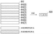
FIG. 8 is a schematic diagram illustrating recording of a bad entity program cell in usage information according to an example embodiment.
Referring to FIG. 8, the physical erase unit 810 includes 8 physical program units (i.e., 0 th to 7 th physical program units). After scanning the physical erase unit 810, the memory control circuit unit 404 (or the memory management circuit 502) determines that the 1 st physical programming unit (i.e., the physical programming unit 810(1)), the 3 rd physical programming unit (i.e., the physical programming unit 810(3)), and the 5 th physical programming unit (i.e., the physical programming unit 810(5)) are bad physical programming units. Therefore, the memory control circuit unit 404 (or the memory management circuit 502) records the usage information 820 for the entity erasing unit 810, and records the values 1, 3, and 5 in the usage information 820 to indicate that the entity programming unit 810(1), the entity programming unit 810(3), and the entity programming unit 810(5) are bad entity programming units.
In the present exemplary embodiment, the values 1, 3, and 5 recorded in the usage information 820 are merely illustrative. In another example embodiment, the memory control circuit unit 404 (or the memory management circuit 502) may record the address offset value corresponding to the bad physical program cell in the physical erase cell 810 in the usage information 820. Herein, the address offset value of a physical programming unit refers to a distance between a start address of the physical programming unit and a start address of a physical erasing unit to which the physical programming unit belongs. Furthermore, the memory control circuit unit 404 (or the memory management circuit 502) can record the bad physical programming unit in the form of Byte (Byte). For example, for a physical erase unit including 256 physical program units (i.e., including 0 th to 255 th physical program units), one physical program unit can be represented by one byte. For example, the byte "00000000" represents that the 0 th entity program unit is a bad entity program unit. In this case, if a physical erase unit includes 8 bad-physical-programming units, the memory control circuit unit 404 (or the memory management circuit 502) records 8 bytes in the use information to indicate the 8 bad-physical-programming units. However, a Bit (Bit) format may also be used to record bad entity program cells. For example, for a physical erase unit comprising 256 physical program units, all the physical program units of a physical erase unit can be recorded with 256 bits (i.e. including bits 0-255), where each bit represents a physical program unit. Assume that a bit value of 1 indicates a bad physical program cell and a bit value of 0 indicates a good physical program cell. If the 5 th bit in the usage information of a physically erased cell is 1, it indicates that the 5 th physically programmed cell of the physically erased cell is a bad physically programmed cell. In this case, whether a physical erase unit includes several bad physical program units, the memory control circuit unit 404 (or the memory management circuit 502) records 256 bits (i.e. 32 bytes) in the use information to represent the bad physical program units. Therefore, the type of the physical program unit to be recorded can be determined according to the actual requirement, and the invention is not limited thereto.
After determining to record the bad or good physical program cells in the usage information, the memory control circuit unit 404 (or the memory management circuit 502) scans all the physical erase cells and records the corresponding usage information for each physical erase cell. The usage information can be recorded in a physically erased cell of the rewritable non-volatile memory, such as a physically erased cell in the system area.
The memory control circuitry 404 (or memory management circuitry 502) may also configure the super entity units according to the recorded usage information. One super-physical cell includes at least two good physical erase cells among all the physical erase cells. Also, the address offset value of the bad-entity programmed cell in one of the good-entity erased cells may be different from the address offset value of the bad-entity programmed cell in the other good-entity erased cells. In other words, the good entity programmed cell of the two good entity erased cells of a super entity cell can be located at a non-corresponding address of the two good entity erased cells. Each of the super-entity units may have a plurality of super-entity programming units. That is, the good physical programming cells located at the non-corresponding addresses of the two physically erased cells may be configured as one of the super physical programming cells. For example, the 1 st, 3 rd, 5 th, and 7 th physical programming cells of one good physical erase cell of a super-physical cell are good, and the 0 th, 2 th, 4 th, and 6 th physical programming cells of another good physical erase cell are good, so that the 1 st physical programming cell of one good physical erase cell and the 0 th physical programming cell of another good physical erase cell can be configured as a super-physical programming cell. In the exemplary embodiment, at least two good erase units included in a super-physical unit belong to different operation units (e.g., planes, interlaces, or channels). Therefore, different physical program cells in a super physical program cell can be programmed simultaneously according to the same write command.
Specifically, the memory control circuit unit 404 (or the memory management circuit 502) calculates the available capacity of the rewritable nonvolatile memory module 406 according to the usage information of all the physically erased units. In more detail, the available capacity is calculated according to the number of good physical program cells in each of the physically erased cells. For example, the memory control circuit unit 404 (or the memory management circuit 502) may calculate the number of good physically programmed cells in each of the physically erased cells according to the usage information of each of the physically erased cells. The memory control circuit unit 404 (or the memory management circuit 502) determines the capacity of each super-physical unit according to the calculated number. In the present exemplary embodiment, the memory control circuit unit 404 (or the memory management circuit 502) can identify the minimum value from the calculated numbers as the capacity of each good erase unit for configuring the super-physical units, and then determine the capacity of each super-physical unit. That is, the capacity of each good erase unit for configuring the super-physical unit is the minimum value among the numbers of good programmed units of all the physical erase units. The capacity of a super-physical cell is equal to the minimum value multiplied by the number of good physical erased cells included in a super-physical cell. In this way, the memory control circuit unit 404 (or the memory management circuit 502) can determine the available capacity according to the number of configured super-physical units and the capacity of each super-physical unit. For example, the available capacity can be calculated by multiplying the capacity of each super entity unit by the number of super entity units.
FIG. 9 is a diagram illustrating calculation of available capacity according to an example embodiment.
Referring to FIG. 9, it is assumed that the rewritable nonvolatile memory module 901 has a physical erase unit 910, a physical erase unit 920, a physical erase unit 930, and a physical erase unit 940, and each physical erase unit has 8 physical program units. The memory control circuit unit 404 (or the memory management circuit 502) determines that the physical-erased cells 910 and the physical-erased cells 920 respectively include 1 bad-physical programmed cell, the physical-erased cells 930 include 3 bad-physical programmed cells, and the physical-erased cells 940 include 4 bad-physical programmed cells according to the usage information of each physical-erased cell. In other words, memory control circuitry unit 404 (or memory management circuitry 502) can calculate that the number of good solid program cells in physically erased cell 910 is 7, the number of good solid program cells in physically erased cell 920 is 7, the number of good solid program cells in physically erased cell 930 is 5, and the number of good solid program cells in physically erased cell 940 is 4. That is, among all the physically erased cells, the physically erased cell 940 has the least good physically programmed cell. Therefore, the memory control circuit unit 404 (or the memory management circuit 502) determines the capacity of one good physically erased cell to be 4 good physically programmed cells. In the present exemplary embodiment, each super-physical cell includes two good erase cells, so that the super-physical cells 950 and 960 can be configured, and each super-physical cell has a capacity of 8 good program cells. Accordingly, the memory control circuit unit 404 (or the memory management circuit 502) can calculate the available capacity of the rewritable nonvolatile memory module 901 to be 16 good physical programming units.
Furthermore, since each of the plurality of physically erased cells has corresponding usage information, the memory control circuit unit 404 (or the memory management circuit 502) can determine the address offset value corresponding to the bad physically programmed cell in each of the plurality of physically erased cells according to the usage information. That is, the memory control circuit unit 404 (or the memory management circuit 502) can configure the super-physical cells by using the physically erased cells including the bad-physical programmed cells with different address offset values. As shown in FIG. 9, the super-physical unit 950 includes a physical erase unit 910 and a physical erase unit 920, wherein the physical program unit 910(3) in the physical erase unit 910 is a bad physical program unit and has a corresponding address offset value of 3, and the physical program unit 920(2) in the physical erase unit 920 is a bad physical program unit and has a corresponding address offset value of 2. That is, the disposed super-solid units, i.e., the solid erase unit 910 and the solid erase unit 920, may include good solid program units corresponding to the same address offset value (e.g., the solid program unit 910(0) in the solid erase unit 910 and the solid program unit 920(0) in the solid erase unit 920) or may include good solid program units corresponding to different address offset values (e.g., the solid program unit 910(2) in the solid erase unit 910 and the solid program unit 920(3) in the solid erase unit 920). Moreover, the address offset value of the bad entity programming unit 910(3) in the entity erasing unit 910 is the same as the address offset value of the good entity programming unit 920(3) in the entity erasing unit 920. In other words, the entity programming unit 910(0) in the entity erasing unit 910 and the entity programming unit 920(0) in the entity erasing unit 920 can be configured as one super entity programming unit of the super entity unit 950, and the entity programming unit 910(2) in the entity erasing unit 910 and the entity programming unit 920(3) in the entity erasing unit 920 can be configured as another super entity programming unit of the super entity unit 950.
In addition, since the capacity of a good physically erased cell is determined according to the minimum value of the number of good physically programmed cells in each of the physically erased cells, some of the good physically programmed cells included in the physically erased cells 910, 920, and 930 belong to the remaining good physically programmed cells. When the write operation of the physical erase cell is performed, the write data is not programmed into the remaining good physical programming.
In some rewritable non-volatile memory modules, data stored in one physical programming unit may be affected by another physical programming unit. For example, in a rewritable nonvolatile memory module in which a plurality of bits can be stored in one memory cell, a plurality of physical program units formed by the same memory cell may affect each other due to a program operation. Therefore, in the present exemplary embodiment, the memory control circuit unit 404 (or the memory management circuit 502) further performs a programming test on at least one physically erased cell, and determines whether to program dummy data (dummy data) to a bad physically programmed cell when performing a write operation according to a result of the programming test.
Specifically, the memory control circuit unit 404 (or the memory management circuit 502) selects at least one physically erased cell to perform the programming test. During the programming test, the memory control circuit unit 404 (or the memory management circuit 502) performs two programming operations on the selected physically erased cells. The test data is programmed into the good physical programming unit in both programming processes. In one of the programming processes, the dummy data is not programmed to the bad entity programming unit, but in the other programming process, the dummy data is programmed to the bad entity programming unit. After each program operation, the memory control circuit unit 404 (or the memory management circuit 502) reads the data stored in the selected physically erased cells and calculates the error bit count of the read data, so as to determine whether to program the dummy data into the bad physically programmed cells during the write operation according to the calculated error bit count after the two program operations.
FIG. 10 is a schematic diagram illustrating performing a programming test according to an example embodiment. In the present exemplary embodiment, it is assumed that one physically erased cell is selected to perform a programming test.
Referring to FIG. 10, the selected entity erased cells 1010 include entity programmed cells 1010(0) -1010 (7), wherein the entity programmed cells 1010(1) and the entity programmed cells 1010(4) are bad entity programmed cells.
The memory control circuitry 404 (or the memory management circuitry 502) performs a first programming of the physically erased cells 1010. During the first programming, the memory control circuit unit 404 (or the memory management circuit 502) only performs the programming for the good physical program unit, and the bad physical program unit is not programmed with any data. In the present exemplary embodiment, the memory control circuit unit 404 (or the memory management circuit 502) programs the test data into all the good physical programming units, and the test data may be any data. Therefore, after the first programming is completed, the good physical programming cells in the physically erased cells 1010' will have valid data, and the bad physical programming cells will not have data. Then, the memory control circuit unit 404 (or the memory management circuit 502) will perform a read command to read the valid data in the physical erase unit 1010', check whether the read valid data has errors, and calculate the error bit count of the valid data to generate a test result. In the present exemplary embodiment, the memory control circuit unit 404 (or the memory management circuit 502) can program the test data into the data bit region of the good physical programming unit and program the corresponding error checking and correcting codes into the redundancy bit region of the good physical programming unit when programming the good physical programming unit. Therefore, the memory control circuit unit 404 (or the memory management circuit 502) can check the read valid data by the error checking and correcting circuit 512 using the error checking and correcting code. In the present exemplary embodiment, according to the test result of the first programming, the memory control circuit unit 404 (or the memory management circuit 502) checks that the valid data read from the good physical programming unit 1010 ' (0), the physical programming unit 1010 ' (2), and the physical programming unit 1010 ' (3) have errors, and calculates the error bit count (hereinafter also referred to as the first error bit count) of the valid data having errors.
Then, the memory control circuit unit 404 (or the memory management circuit 502) erases the data stored in the physically erased cell 1010' to perform the second programming. During the second programming, the memory control circuit unit 404 (or the memory management circuit 502) programs the test data into the good physical programming unit and programs the dummy data into the bad physical programming unit. After the second programming is completed, the good physical program cells in the physically erased cells 1010 ″ will have valid data, and the bad physical program cells will have dummy data. Next, the physical erase unit 1010 "memory control circuit unit 404 (or the memory management circuit 502) reads and checks the valid data stored in the physical erase unit 1010". In the present exemplary embodiment, based on the test result of the second programming, the memory control circuit unit 404 (or the memory management circuit 502) checks that the valid data of the good physical programming unit 1010 "(3) has an error, and calculates an error bit count (hereinafter also referred to as a second error bit count) of the valid data having the error.
Further, the memory control circuit unit 404 (or the memory management circuit 502) compares the first error bit count with the second error bit count. If the first faulty bit count is greater than the second faulty bit count, it indicates that programming the dummy data into the bad entity program unit will reduce the probability of the valid data being faulty. Therefore, the memory control circuit unit 404 (or the memory management circuit 502) determines to program the dummy data into the bad physical programming unit of the physically erased units when performing the write operation. In contrast, if the first faulty bit count is not greater than the second faulty bit count, it indicates that programming the dummy data into the bad entity program cell increases the probability of the valid data being faulty. Therefore, the memory control circuit unit 404 (or the memory management circuit 502) determines not to program the dummy data into the bad physical programming unit of the physically erased units when performing the write operation.
In the present exemplary embodiment, the memory control circuit unit 404 (or the memory management circuit 502) can calculate the sum of the number of error bits of each valid data in the physically erased cells as the error bit count corresponding to the physically erased cells. However, the invention is not limited thereto, and the memory control circuit unit 404 (or the memory management circuit 502) may also calculate an average value of the number of error bits of each valid data in the physically erased cells as the error bit count corresponding to the physically erased cells.
In addition, in another exemplary embodiment, a plurality of physically erased cells may be selected to perform the programming test. For example, the sum of all the first error bit counts and the sum of all the second error bit counts of the selected physically erased cells are compared. Alternatively, the average of all the first error bit counts of the selected physically erased cells is compared with the average of all the second error bit counts. The invention does not limit the way the error bit count is calculated.
FIG. 11 is a flowchart illustrating a memory management method according to an example embodiment.
In step S1101, the memory control circuit unit 404 (or the memory management circuit 502) records the usage information for each physically erased cell in the rewritable nonvolatile memory module 406.
In step S1103, the memory control circuit unit 404 (or the memory management circuit 502) calculates the number of good physical program cells in each physical erase cell according to the recorded usage information.
In step S1105, the memory control circuit unit 404 (or the memory management circuit 502) determines the capacity of each super entity unit according to the minimum value of the calculated numbers.
In step S1107, the memory control circuit unit 404 (or the memory management circuit 502) configures a plurality of super-physical units according to the recorded usage information, wherein each super-physical unit includes at least two physical erase units, and the address offset value of at least one good physical program unit in one of the physical erase units of at least one super-physical unit is the same as the address offset value of at least one bad physical program unit in another physical erase unit. That is, the address offset values of the at least two physically erased cells corresponding to the bad physically programmed cells may be different from each other.
In step S1109, the memory control circuit unit 404 (or the memory management circuit 502) determines the available capacity corresponding to the rewritable nonvolatile memory module 406 according to the number of configured super-physical units and the capacity of each super-physical unit.
FIG. 12 is a flowchart illustrating steps of recording usage information in a memory management method according to an example embodiment.
In step S1201, the memory control circuit unit 404 (or the memory management circuit 502) scans the number of good physically programmed cells of at least one physically erased cell in the rewritable nonvolatile memory module 406.
In step S1203, the memory control circuit unit 404 (or the memory management circuit 502) determines whether the number of good physical programming units of the at least one physical erase unit is greater than the identification threshold number.
If the number is greater than the identification threshold number, in step S1205, the memory control circuit unit 404 (or the memory management circuit 502) records the bad physical program cells in each of the physical erase cells in the usage information.
If the number is not greater than the identification threshold number, in step S1207, the memory control circuit unit 404 (or the memory management circuit 502) records the good physical program cells in each of the physical erase cells in the usage information.
FIG. 13 is a flowchart illustrating a process of determining whether to write dummy data to a bad physical program cell according to an example embodiment.
In step S1301, the memory control circuit unit 404 (or the memory management circuit 502) selects at least one physical erase unit to perform a programming test on the selected physical erase unit.
Then, the memory control circuit unit 404 (or the memory management circuit 502) performs a first programming on the selected physically erased cells. That is, in step S1303, the memory control circuit unit 404 (or the memory management circuit 502) programs the test data into the good physical programming cells of the selected physical erase cells without programming the bad physical programming cells.
In step S1305, the memory control circuit unit 404 (or the memory management circuit 502) reads the test data from the good physically programmed cells of the selected physically erased cells, and calculates an error bit count (hereinafter also referred to as a first error bit count) of the read test data.
Then, the memory control circuit unit 404 (or the memory management circuit 502) performs a second programming on the selected physically erased cells. That is, in step S1307, the memory control circuit unit 404 (or the memory management circuit 502) programs the test data into good physical programming cells of the selected physically erased cells and programs the dummy data into bad physical programming cells of the selected physically erased cells. Before performing this step, the memory control circuit unit 404 (or the memory management circuit 502) may also perform an erase operation on the selected physically erased cells to erase the data stored in the selected physically erased cells.
In step S1309, the memory control circuit unit 404 (or the memory management circuit 502) reads the test data from the good physical programming unit of the selected physical erase unit, and calculates an error bit count (hereinafter also referred to as a second error bit count) of the read test data. The manner of calculating the error bit count is described in detail in the foregoing, and is not described herein again.
In step 1311, the memory control circuit unit 404 (or the memory management circuit 502) determines whether the first erroneous bit count is greater than the second erroneous bit count.
If the first error bit count is greater than the second error bit count, in step 1313, dummy data is programmed into a bad physical program cell of the physically erased cells while performing the write operation.
If the first faulty bit count is not greater than the second faulty bit count, bad physical program cells of the physically erased cells are not programmed while performing the write operation in step 1315.
In the exemplary embodiment, during the programming test, the memory control circuit unit 404 (or the memory management circuit 502) does not program the bad-erase cells during the first programming, and then programs the dummy data into the bad-erase cells during the second programming. However, in another exemplary embodiment, the memory control circuit unit 404 (or the memory management circuit 502) may also program the dummy data to the bad-erase cells during the first programming and then not program the bad-erase cells during the second programming.
In summary, the bad entity programmed cells in each entity erased cell can be correctly identified by recording the use information for each entity erased cell in the rewritable nonvolatile memory module. Therefore, the address offset values of the corresponding bad-entity programmed cells in each entity-erased cell can be different from each other, thereby reducing the number of the entity-erased cells which are judged to be bad-entity-erased cells and determining more available capacity. In addition, the address offset values of the respective bad-erase units in the at least two physically-erased units included in the super-physical units configured by the recorded usage information may be different from each other, so that the super-physical units are more flexible in memory management.
Although the present invention has been described with reference to the above embodiments, it should be understood that the invention is not limited to the embodiments, and various changes and modifications can be made by one skilled in the art without departing from the spirit and scope of the invention.
Claims (15)
1. A memory management method is used for a rewritable nonvolatile memory module, the rewritable nonvolatile memory module comprises a plurality of entity erasing units, each entity erasing unit comprises a plurality of entity programming units, and the memory management method comprises the following steps:
recording a plurality of use information according to each of the plurality of physically erased units, wherein each of the plurality of use information is used for indicating a non-available physically programmed unit or an available physically programmed unit of each physically erased unit;
calculating an available capacity according to the plurality of usage information, wherein the available capacity is calculated according to the number of available physically-erased cells in each of the plurality of physically-erased cells; and
configuring a plurality of super-physical cells according to the plurality of usage information, wherein each of the plurality of super-physical cells includes at least two of the plurality of physically-erased cells,
wherein the plurality of super-physical cells include a first super-physical cell including a first physically erased cell including a first non-usable physically programmed cell and a second physically erased cell including a first usable physically programmed cell, and an address offset value corresponding to the first non-usable physically programmed cell in the first physically erased cell is the same as an address offset value corresponding to the first usable physically programmed cell in the second physically erased cell,
wherein the step of calculating the available capacity from the plurality of usage information comprises:
calculating the number of available physical programming units of each physical erasing unit according to the plurality of using information;
determining a capacity of each super-physical cell according to a minimum value among the number of available physical programming cells of the plurality of physical erase cells; and
and determining the available capacity according to the number of the plurality of super-entity units and the capacity of each super-entity unit.
2. The method of claim 1, wherein each super-physical cell comprises a plurality of super-physical programming cells, the first physical erase cell comprises a second available physical programming cell, wherein the second available physical programming cell of the first physical erase cell and the first available physical programming cell of the second physical erase cell are configured as one super-physical programming cell of the first super-physical cell, and wherein an address offset value corresponding to the second available physical programming cell in the first physical erase cell is different from the address offset value corresponding to the first available physical programming cell in the second physical erase cell.
3. The method according to claim 1, wherein the step of recording the usage information for each physically erased cell of the plurality of physically erased cells comprises:
scanning the number of available physical programming units of the at least one physical erasing unit;
if the number of the available physical programming units of the at least one physical erasing unit is not more than the identification threshold number, recording the available physical programming units in the plurality of physical erasing units in the plurality of use information; and
if the number of available physical programming units of the at least one physical erasing unit is larger than the identification threshold number, recording non-available physical programming units in the plurality of physical erasing units in the plurality of use information.
4. The memory management method of claim 3, further comprising:
recording an identification flag to mark whether the physical program unit recorded in the plurality of usage information is an available physical program unit or a non-available physical program unit.
5. The memory management method of claim 1, further comprising:
selecting at least one physically erased cell from the plurality of physically erased cells, wherein the at least one physically erased cell includes a plurality of available physically programmed cells and a plurality of unavailable physically programmed cells;
programming test data into available physical programming cells of the at least one physically erased cell without programming non-available physical programming cells of the at least one physically erased cell, reading data from the available physical programming cells of the at least one physically erased cell, and calculating the number of error bits in the read data as a first error bit count;
programming the test data into available physical programming cells of the at least one physically erasable cell, programming dummy data into non-available physical programming cells of the at least one physically erasable cell, reading data from the available physical programming cells of the at least one physically erasable cell, and calculating the number of error bits in the read data as a second error bit count; and
and programming the dummy data to a non-available physical programming cell of the plurality of physically erased cells when performing a write operation if the first error bit count is greater than the second error bit count.
6. A memory control circuit unit, configured to control a rewritable nonvolatile memory module, where the rewritable nonvolatile memory module includes a plurality of physical erase units, each physical erase unit includes a plurality of physical programming units, and the memory control circuit unit includes:
a host interface for electrically connecting to a host system;
a memory interface for electrically connecting to the rewritable nonvolatile memory module; and
a memory management circuit electrically connected to the host interface and the memory interface,
wherein the memory management circuit is used for recording a plurality of usage information according to each of the plurality of physically erased units, wherein each of the plurality of usage information is used for indicating a non-available physically programmed unit or an available physically programmed unit of each physically erased unit,
wherein the memory management circuit is further configured to calculate an available capacity according to the usage information, wherein the available capacity is calculated according to a number of available physically-erased cells in each of the plurality of physically-erased cells,
wherein the memory management circuit is further configured to configure a plurality of super-physical cells according to the usage information, wherein each of the super-physical cells includes at least two of the plurality of physically-erased cells,
wherein the plurality of super-physical cells include a first super-physical cell including a first physically erased cell and a second physically erased cell, the first physically erased cell includes a first non-usable physically programmed cell, the second physically erased cell includes a first usable physically programmed cell, and an address offset value corresponding to the first non-usable physically programmed cell in the first physically erased cell is the same as an address offset value corresponding to the first usable physically programmed cell in the second physically erased cell,
wherein the memory management circuit is further configured to calculate a number of available physical programming cells per physically erased cell based on the plurality of usage information,
wherein the memory management circuit is further configured to determine a capacity of each super-physical cell according to a minimum value among a number of available physical programming cells of the plurality of physically erased cells,
wherein the memory management circuit is further configured to determine the available capacity according to the number of the plurality of super-physical units and a capacity of each super-physical unit.
7. The memory control circuit unit of claim 6, wherein each super-physical cell comprises a plurality of super-physical programming cells, the first physical erase cell comprises a second available physical programming cell, wherein the second available physical programming cell of the first physical erase cell and the first available physical programming cell of the second physical erase cell are configured as one super-physical programming cell of the first super-physical cell, and wherein an address offset value corresponding to the second available physical programming cell in the first physical erase cell is different from the address offset value corresponding to the first available physical programming cell in the second physical erase cell.
8. The memory control circuit unit of claim 6, wherein the memory management circuit is further configured to scan the number of available physical programming cells in the at least one physically erased cell,
wherein if the number of available physical programming cells of the at least one physically-erased cell is not greater than the identification threshold number, the memory management circuit is further configured to record the available physical programming cells of the plurality of physically-erased cells in the plurality of usage information,
wherein if the number of available physical programming cells of the at least one physically-erased cell is greater than the identification threshold number, the memory management circuit is further configured to record non-available physical programming cells of the plurality of physically-erased cells in the plurality of usage information.
9. The memory control circuit unit of claim 8, wherein the memory management circuit is further configured to record an identification flag to mark whether the physical program unit recorded in the usage information is an available physical program unit or a non-available physical program unit.
10. The memory control circuit unit of claim 6, wherein the memory management circuit is further configured to select at least one physically-erased cell from the plurality of physically-erased cells, wherein the at least one physically-erased cell includes a plurality of available physically-programmed cells and a plurality of unavailable physically-programmed cells,
wherein the memory management circuit is further configured to program test data into available ones of the at least one physically erased cell without programming non-available ones of the at least one physically erased cell, read data from available ones of the at least one physically erased cell, calculate a number of erroneous bits in the read data as a first erroneous bit count,
wherein the memory management circuit programs the test data into available ones of the at least one physically erased cell, programs dummy data into non-available ones of the at least one physically erased cell, reads data from the available ones of the at least one physically erased cell, calculates a number of erroneous bits in the read data as a second erroneous bit count,
wherein if the first error bit count is greater than the second error bit count, the memory management circuit is further configured to program the dummy data to a non-available physical programming cell of the plurality of physical erase cells when performing a write operation.
11. A memory storage device, comprising:
the connection interface unit is used for electrically connecting to a host system;
the rewritable nonvolatile memory module comprises a plurality of entity erasing units; and
a memory control circuit unit electrically connected to the connection interface unit and the rewritable nonvolatile memory module,
wherein the memory control circuit unit is used for recording a plurality of usage information according to each of the plurality of physically erased units, wherein each of the plurality of usage information is used for indicating a non-available physically programmed unit or an available physically programmed unit of each physically erased unit,
wherein the memory control circuit unit is further configured to determine an available capacity according to the usage information, wherein the available capacity is based on a number of available physical program cells in each of the plurality of physically erased cells,
wherein the memory control circuit unit is further configured to configure a plurality of super-physical units according to the plurality of usage information, wherein each of the plurality of super-physical units includes at least two of the plurality of physically-erased units,
wherein the plurality of super-physical cells include a first super-physical cell including a first physically erased cell and a second physically erased cell, the first physically erased cell includes a first non-usable physically programmed cell, the second physically erased cell includes a first usable physically programmed cell, and an address offset value corresponding to the first non-usable physically programmed cell in the first physically erased cell is the same as an address offset value corresponding to the first usable physically programmed cell in the second physically erased cell,
wherein the memory control circuit unit is further configured to calculate a number of available physical programming cells per physically erased cell based on the plurality of usage information,
wherein the memory control circuit unit is further configured to determine a capacity of each super-physical unit according to a minimum value among the number of available physical programming units of the plurality of physical erase units,
the memory control circuit unit is further configured to determine the available capacity according to the number of the plurality of super-physical units and the capacity of each super-physical unit.
12. The memory storage device of claim 11, wherein each super-physical cell comprises a plurality of super-physical programming cells, the first physical erase cell comprises a second available physical programming cell, wherein the second available physical programming cell of the first physical erase cell and the first available physical programming cell of the second physical erase cell are configured as one super-physical programming cell of the first super-physical cell, and wherein an address offset value corresponding to the second available physical programming cell in the first physical erase cell is different from the address offset value corresponding to the first available physical programming cell in the second physical erase cell.
13. The memory storage device of claim 11, wherein the memory control circuit unit is further configured to scan a number of available physically programmed cells of the at least one physically erased cell,
wherein if the number of available physical programming cells of the at least one physically-erased cell is not greater than the identification threshold number, the memory control circuit unit is further configured to record the available physical programming cells of the plurality of physically-erased cells in the plurality of usage information,
wherein if the number of available physical programming cells of the at least one physically-erased cell is greater than the identification threshold number, the memory control circuit unit is further configured to record non-available physical programming cells of the plurality of physically-erased cells in the plurality of usage information.
14. The memory storage device of claim 13, wherein the memory control circuit unit is further configured to record an identification flag to mark whether the physical program unit recorded in the usage information is an available physical program unit or a non-available physical program unit.
15. The memory storage device according to claim 11, wherein the memory control circuit unit is further configured to select at least one physically-erased cell from the plurality of physically-erased cells, wherein the at least one physically-erased cell comprises a plurality of available physically-programmed cells and a plurality of unavailable physically-programmed cells,
wherein the memory control circuit unit is further configured to program test data into available ones of the at least one physically erased cell without programming non-available ones of the at least one physically erased cell, read data from available ones of the at least one physically erased cell, calculate a number of erroneous bits in the read data as a first erroneous bit count,
wherein the memory control circuit unit programs the test data into available ones of the at least one physically erased cell, programs dummy data into non-available ones of the at least one physically erased cell, reads data from the available ones of the at least one physically erased cell, calculates the number of erroneous bits in the read data as a second erroneous bit count,
wherein if the first error bit count is greater than the second error bit count, the memory control circuit unit is further configured to program the dummy data to a non-available physical programming cell of the plurality of physical erase cells when performing a write operation.
Priority Applications (1)
| Application Number | Priority Date | Filing Date | Title |
|---|---|---|---|
| CN201610003016.7A CN106940623B (en) | 2016-01-04 | 2016-01-04 | Memory management method, memory control circuit unit and memory storage device |
Applications Claiming Priority (1)
| Application Number | Priority Date | Filing Date | Title |
|---|---|---|---|
| CN201610003016.7A CN106940623B (en) | 2016-01-04 | 2016-01-04 | Memory management method, memory control circuit unit and memory storage device |
Publications (2)
| Publication Number | Publication Date |
|---|---|
| CN106940623A CN106940623A (en) | 2017-07-11 |
| CN106940623B true CN106940623B (en) | 2020-06-09 |
Family
ID=59469833
Family Applications (1)
| Application Number | Title | Priority Date | Filing Date |
|---|---|---|---|
| CN201610003016.7A Active CN106940623B (en) | 2016-01-04 | 2016-01-04 | Memory management method, memory control circuit unit and memory storage device |
Country Status (1)
| Country | Link |
|---|---|
| CN (1) | CN106940623B (en) |
Citations (4)
| Publication number | Priority date | Publication date | Assignee | Title |
|---|---|---|---|---|
| CN102341793A (en) * | 2009-03-04 | 2012-02-01 | 美光科技公司 | Memory block selection |
| CN102473091A (en) * | 2009-07-01 | 2012-05-23 | 超威半导体公司 | Extended page size using aggregated small pages |
| CN102479156A (en) * | 2010-11-22 | 2012-05-30 | 慧荣科技股份有限公司 | Method for carrying out block management and memory device and controller thereof |
| CN103593255A (en) * | 2012-08-15 | 2014-02-19 | 群联电子股份有限公司 | Data management method, memory storage and memory storage controller |
Family Cites Families (1)
| Publication number | Priority date | Publication date | Assignee | Title |
|---|---|---|---|---|
| US8832507B2 (en) * | 2010-08-23 | 2014-09-09 | Apple Inc. | Systems and methods for generating dynamic super blocks |
-
2016
- 2016-01-04 CN CN201610003016.7A patent/CN106940623B/en active Active
Patent Citations (4)
| Publication number | Priority date | Publication date | Assignee | Title |
|---|---|---|---|---|
| CN102341793A (en) * | 2009-03-04 | 2012-02-01 | 美光科技公司 | Memory block selection |
| CN102473091A (en) * | 2009-07-01 | 2012-05-23 | 超威半导体公司 | Extended page size using aggregated small pages |
| CN102479156A (en) * | 2010-11-22 | 2012-05-30 | 慧荣科技股份有限公司 | Method for carrying out block management and memory device and controller thereof |
| CN103593255A (en) * | 2012-08-15 | 2014-02-19 | 群联电子股份有限公司 | Data management method, memory storage and memory storage controller |
Also Published As
| Publication number | Publication date |
|---|---|
| CN106940623A (en) | 2017-07-11 |
Similar Documents
| Publication | Publication Date | Title |
|---|---|---|
| US10713178B2 (en) | Mapping table updating method, memory controlling circuit unit and memory storage device | |
| US10437484B2 (en) | Data protecting method, memory control circuit unit and memory storage device | |
| US10579289B2 (en) | Memory management method for configuring super physical units of rewritable non-volatile memory modules, memory control circuit unit and memory storage device | |
| US8301981B2 (en) | Data access method for flash memory and storage system and controller thereof | |
| CN111078146B (en) | Memory management method, memory storage device and memory control circuit unit | |
| CN107045890B (en) | Data protection method, memory control circuit unit and memory storage device | |
| CN109273033B (en) | Memory management method, memory control circuit unit and memory storage device | |
| CN107204205B (en) | Memory management method, memory control circuit unit and memory storage device | |
| CN113138720A (en) | Data storage method, memory control circuit unit and memory storage device | |
| CN107103930B (en) | Data writing method, memory control circuit unit and memory storage device | |
| CN106354651B (en) | Average wear method, memory control circuit unit and memory storage device | |
| CN110275668B (en) | Block management method, memory control circuit unit and memory storage device | |
| CN114822664B (en) | Risk assessment method based on data priority, storage device and control circuit | |
| CN110442299B (en) | Data writing method, memory control circuit unit and memory storage device | |
| CN109032957B (en) | Memory management method, memory control circuit unit and memory storage device | |
| US11609822B2 (en) | Data storing method, memory control circuit unit and memory storage device | |
| CN107132989B (en) | Data programming method, memory control circuit unit and memory storage device | |
| US10067677B2 (en) | Memory management method for configuring super physical units of rewritable non-volatile memory modules, memory control circuit unit and memory storage device | |
| CN111831210B (en) | Memory management method, memory control circuit unit and memory storage device | |
| CN106920572B (en) | Memory management method, memory control circuit unit and memory storage device | |
| CN106940623B (en) | Memory management method, memory control circuit unit and memory storage device | |
| CN109522236B (en) | Memory management method, memory control circuit unit and memory storage device | |
| CN108958640B (en) | Memory management method, memory control circuit unit and memory storage device | |
| CN111610937A (en) | Data writing method, memory storage device and memory control circuit unit | |
| CN106970763B (en) | Memory management method, memory control circuit unit and memory storage device |
Legal Events
| Date | Code | Title | Description |
|---|---|---|---|
| PB01 | Publication | ||
| PB01 | Publication | ||
| SE01 | Entry into force of request for substantive examination | ||
| SE01 | Entry into force of request for substantive examination | ||
| GR01 | Patent grant | ||
| GR01 | Patent grant |