CN1069134C - Gas sensor for detecting nitrogen dioxide and its prodn technology - Google Patents
Gas sensor for detecting nitrogen dioxide and its prodn technology Download PDFInfo
- Publication number
- CN1069134C CN1069134C CN 96102646 CN96102646A CN1069134C CN 1069134 C CN1069134 C CN 1069134C CN 96102646 CN96102646 CN 96102646 CN 96102646 A CN96102646 A CN 96102646A CN 1069134 C CN1069134 C CN 1069134C
- Authority
- CN
- China
- Prior art keywords
- field effect
- effect transistor
- chip
- film
- monomolecular film
- Prior art date
- Legal status (The legal status is an assumption and is not a legal conclusion. Google has not performed a legal analysis and makes no representation as to the accuracy of the status listed.)
- Expired - Fee Related
Links
Images

Landscapes
- Investigating Or Analyzing Materials By The Use Of Electric Means (AREA)
- Thin Film Transistor (AREA)
Abstract
The present invention relates to a hanging grid field effect type gas sensor for detecting the LB film decoration of NO2, and a manufacture method thereof. The gas sensor has the structure that a hanging grid field effect transistor comprises an LB film of cobalt porphyrin quaternary ammonium or phthalocyanine copper sulfuret or derivatives thereof, which is drawn on the whole surface of a gate region. The present invention comprises the following manufacture processes: a chip of the hanging grid field effect transistor is drawn in liquid floated with the LB film, so that the LB film is attached to the surface of the chip and is dried in vacuum; the film is repeatedly drawn and dried, so that the LB film reaches appropriate thickness and is cut into individual chips to lead AL electrodes. The gas sensor of the present invention has the advantages of high sensitivity, good selectivity, rapid response, good consistency and simple technology, and is suitable for bulk production.
Description
The invention belongs to a kind of gas sensor, outstanding gate field-effect type gas sensor and manufacture craft thereof that particularly a kind of organic supramolecular is film modified.
Outstanding gate field-effect (SGFET) type gas sensor is a kind ofly to modify grid region in field effect transistor with gas sensitive, utilizing gas sensitive to adsorb the CHARGE DISTRIBUTION that forms behind a certain gas changes and changes the semi-conductive surface potential in grid region, thereby cause the variation of field effect transistor gate voltage, a kind of gas sensor that causes the leakage current that detects to change.
The prior art the most approaching with the present invention is that one piece of document is disclosed, and the document exercise question is " identification H
2And NH
3Outstanding grid field effect transistor (Recognition of the Hydrogenand Ammonia by Modified Gate Metallijation of the Suspended-gate FET), carry " Sensorsand Actuators " 1990, (B1): 21.Prepared gas sensor is to finish on traditional n ditch enhancement mode field effect transistor, and except the grid region did not have metal level and gate electrode, other structure was consistent with field effect transistor, made gas sensitive SnO then
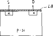
2Only be deposited on the grid region of field effect transistor.We claim not evaporated metal layer of position, grid region, and the field effect transistor of not drawing gate electrode is outstanding grid field effect transistor.The gas sensor configuration of the outstanding gate field-effect type of prior art is provided by Fig. 1.Two places spread certain density n type charge carrier on P type Si substrate, form the drain-source zone, respectively draw source electrode s and drain electrode D in the n district, and promptly the AL electrode constitutes outstanding grid field effect transistor.Grid region surface deposition between two n districts has SnO
2Layer.The technological process of making this gas sensor is roughly, and at first utilizes conventional methods of making semiconductor devices to make the chip of the outstanding grid field effect transistor tube core of enhancement mode, the cutting of demarcating.Described description cutting is exactly to demarcate by die site on chip, cuts apart tube core one by one, but tube core is separated, and each tube core still connects together, and chip is still as a whole, so that the deposition gas sensitive.Then, use special technology simultaneously at the transition metal of each surface, tube core grid region evaporation gas sensing property or stupalith (as SnO
2).At last, chip is divided into single tube core, each tube core is all drawn source electrode S and drain electrode D.
This SnO
2The gas sensor of-SGFET structure is low in energy consumption owing to do not add grid bias, and variable signal is convenient to detect, and it is integrated that device is easy to realize, and consistance is better.But, because gas sensing property transition metal or stupalith generally need just have the ability of stronger adsorbed gas under high temperature, so this transducer sensitivity is lower at normal temperatures; Because transition metal or ceramic gas sensitive are all responsive to multiple gases, cause detection inaccurate so selectivity is relatively poor; Owing to adopt enhancement mode field effect transistor, to can cause just under higher gas concentration that generally tangible leakage current changes, thereby the gas of unfavorable detection low concentration.And in its manufacture craft only at grid region surface deposition (evaporation) gas sensitive, thereby make cumbersome, difficult.
The present invention has designed a kind of with the film modified outstanding gate field-effect type gas sensor of organic supramolecular, organic supramolecular is film modified in whole tube core, and reaching under the gas sensor normal temperature work, sensitivity is higher, selectivity good, can detect the gas of low concentration, and the better simply purpose of technology.
The field effect type gas sensor that organic supramolecular of the present invention is film modified, organic monomolecular film (also claiming the LB film) employing cobalt porphyrin quaternary amine and derivant thereof or sulfuration CuPc and derivant thereof are the organic monomolecular film of feedstock production, and the film modified gas sensor that makes in field effect transistor of these two kinds of raw material LB is used to detect NO
2Gas.This gas sensor can be described as the gas sensor of LB-SGFET structure.
Concrete structure of the present invention is referring to Fig. 2.The surface, grid region of not having the field effect transistor (promptly outstanding grid field effect transistor) of metal level and gate electrode in the grid region draws the organic monomolecular film that cobalt porphyrin quaternary amine or sulfuration CuPc or their derivant are arranged.Outstanding grid field effect transistor promptly spreads the n district that two n type charge carriers are arranged among Fig. 2 on P type Si substrate, and with organic monomolecular film, two n districts draw source electrode S and drain electrode D respectively on the whole surface that comprises the grid region.
The raw material of preparation organic monomolecular film is the four pairs of dimethylamino cobalt porphyrin quaternary amine or derivatives thereofs or four-4-(2,4-two tert-amylbenzene sulfenyls) CuPc or derivatives thereof preferably.They are to NO
2Gas is more responsive, thereby can improve the sensitivity and the selectivity of gas sensor.
The thickness of organic monomolecular film should be suitable on the gas sensor of preparation.To NO
2The sensor of gas, the LB film thickness can be 6~60nm, is preferably 15~45nm.When preparing the LB film with aforesaid cobalt porphyrin quaternary amine, sulfuration CuPc or their derivant, the number of plies on the outstanding grid field effect transistor of control is approximately 4~40 layers, can accomplish that LB film gross thickness is 6~60nm.The number of plies is very few to be unfavorable for obtaining higher sensitivity, and the number of plies too much is unfavorable for responding fast and stability.
The film modified field effect type gas sensor of this LB can adopt enhancement mode to hang grid field effect transistor, also can adopt depletion type to hang grid field effect transistor.Their detect scope different, the NO that can detect lower concentration of depletion type
2Gas promptly has higher sensitivity; Having of enhancement mode is stable preferably.Can use this two kinds of gas sensors according to varying environment in the actual detected.
The film modified outstanding gate field-effect type gas sensor of LB of the present invention is to make like this:
At first, routinely method for making is made the die chip of outstanding grid field effect transistor, by the singulated dies cutting of demarcating, chip is carried out hydrophilic treatment with scribing machine; Method for making prepares the organic monomolecular film of cobalt porphyrin quaternary amine or derivatives thereof or sulfuration CuPc or derivatives thereof routinely, afterwards,
A. chip is placed on and floats in the liquid that organic monomolecular film is arranged, under (20 ± 2) ℃ condition, organic monomolecular film is drawn on the surface, grid region of chip;
B. chip is placed 10
-2Dry under the vacuum tightness of Torr, put into again and float in the liquid that organic monomolecular film is arranged, draw second layer organic monomolecular film;
C. by the process of above-mentioned A, B repeatedly, make the thickness of the multilayer organic monomolecular film on surface, grid region on the chip reach 6~60nm, dry again.
At last, chip is divided into single tube core, uses the static voltage soldering method, form the AL lead-in wire in the drain-source zone (two n districts) of outstanding grid field effect transistor.
The aforesaid organic monomolecular film for preparing according to a conventional method promptly is the method for existing preparation LB film.Generally be that micro mist (as cobalt porphyrin quaternary amine) with raw material is dissolved in organic flux such as the chlorine mill, drop on the liquid surface with the drop mode, such as dropping on the water surface pushing film forming again.
The gas sensor of LB-SGFET structure of the present invention causes the variation of leakage current because the order of LB film after its adsorption gas molecule also exchanges electronics with it, forms dipole layer, thereby produces additional electric field in the grid region in the film.Just because the order of LB film makes gas sensor that high sensitivity be arranged; When particularly adopting depletion field effect transistor, the very little gate voltage that causes in lower gas concentration changes, and also can reflect from leakage current changes, and makes the gas concentration of detection reach the PPb level.Because the material of distinctive preparation LB film of the present invention adsorbs NO again
2Gas molecule also exchanges electronics with it, thereby has high selectivity.Because the ultra-thin characteristic of LB film is rapid to the response and the recovery of gas, thereby the gas sensor of LB film has the characteristics of quick response and fast quick-recovery.Because the LB film directly draws on the chip of outstanding grid field effect transistor, does not need optionally to be deposited on the grid region, and technology is become simply, the making of device also can realize integrated, has good consistance, thereby is convenient to produce in enormous quantities.
Description of drawings:
Fig. 1 is the outstanding grid field effect transistor structural representation of identification hydrogen and ammonia.
Fig. 2 is the gas sensor configuration synoptic diagram of detection nitrogen dioxide of the present invention.
Claims (3)
1, a kind ofly is used to detect NO
2Gas sensor, its structure includes, diffusion has the outstanding grid field effect transistor in the n district of two n type charge carriers on P type Si substrate, two n districts draw active electrode (S) and drain electrode (D) respectively, it is characterized in that, with organic monomolecular film (LB), this organic monomolecular film (LB) is a raw material with cobalt porphyrin quaternary amine and derivant thereof or sulfuration CuPc and derivant thereof on the surface of outstanding grid field effect transistor; The number of plies of organic monomolecular film (LB) is 4~40 layers, and thickness is 6~60nm; Said outstanding grid field effect transistor is outstanding grid field effect transistor of enhancement mode or the outstanding grid field effect transistor of depletion type.
2, be used to detect NO according to claim 1 is described
2Gas sensor, it is characterized in that said organic monomolecular film (LB) is with four pairs of dimethylamino cobalt porphyrin quaternary amine or derivatives thereofs, or four-4-(2,4 two tert-amylbenzene sulfenyl) CuPc or derivatives thereof is a raw material; Its thickness is 15~45nm.
3, a kind of claim 1 is described is used to detect NO
2The manufacture craft of gas sensor, method is at first routinely made the die chip of outstanding grid field effect transistor, by the singulated dies cutting of demarcating, chip is carried out hydrophilic treatment with scribing machine; Adopt conventional method to prepare organic monomolecular film, that is, the micro mist of making the pleurodiaphragmatic in terspace material is dissolved in organic solvent, drop in pushing film forming on the liquid surface with the drop mode again; At last chip is divided into singulated dies, form drain electrode and source contact conductor with the static voltage soldering method in the drain-source zone of outstanding grid field effect transistor, it is characterized in that, after chip is carried out hydrophilic treatment, surface, grid region at outstanding grid field effect transistor draws organic monomolecular film, and its process is divided into;
A, chip is placed on floats in the liquid that organic monomolecular film is arranged, under (20 ± 2) ℃ condition, organic monomolecular film is drawn on the surface, grid region of chip;
B, chip is placed 10
-2Dry under the vacuum tightness of Torr, draw second layer organic monomolecular film again;
C, press A, B process repeatedly, make the thickness of the multilayer organic monomolecular film on surface, grid region on the chip reach 6~60nm, be divided into singulated dies dress AL lead-in wire after the drying.
Priority Applications (1)
| Application Number | Priority Date | Filing Date | Title |
|---|---|---|---|
| CN 96102646 CN1069134C (en) | 1996-02-02 | 1996-02-02 | Gas sensor for detecting nitrogen dioxide and its prodn technology |
Applications Claiming Priority (1)
| Application Number | Priority Date | Filing Date | Title |
|---|---|---|---|
| CN 96102646 CN1069134C (en) | 1996-02-02 | 1996-02-02 | Gas sensor for detecting nitrogen dioxide and its prodn technology |
Publications (2)
| Publication Number | Publication Date |
|---|---|
| CN1147636A CN1147636A (en) | 1997-04-16 |
| CN1069134C true CN1069134C (en) | 2001-08-01 |
Family
ID=5117660
Family Applications (1)
| Application Number | Title | Priority Date | Filing Date |
|---|---|---|---|
| CN 96102646 Expired - Fee Related CN1069134C (en) | 1996-02-02 | 1996-02-02 | Gas sensor for detecting nitrogen dioxide and its prodn technology |
Country Status (1)
| Country | Link |
|---|---|
| CN (1) | CN1069134C (en) |
Cited By (2)
| Publication number | Priority date | Publication date | Assignee | Title |
|---|---|---|---|---|
| CN1325921C (en) * | 2005-05-27 | 2007-07-11 | 东南大学 | Anti-radiation electric field microsensor |
| CN1330968C (en) * | 2005-05-27 | 2007-08-08 | 东南大学 | Micro electric field sensor based on P-type metal-oxide transistor structure |
Families Citing this family (7)
| Publication number | Priority date | Publication date | Assignee | Title |
|---|---|---|---|---|
| EP1457773B1 (en) * | 2001-12-20 | 2006-05-03 | Makoto Yuasa | Electrode for active oxygen species and sensor using the electrode |
| DE102004013678A1 (en) * | 2004-03-18 | 2005-10-20 | Micronas Gmbh | Device for detecting a gas or gas mixture |
| DE102004019604A1 (en) * | 2004-04-22 | 2005-11-17 | Siemens Ag | Method for minimizing cross sensitivities in FET based gas sensors |
| CN102221569B (en) * | 2011-03-25 | 2013-06-05 | 中国科学院长春应用化学研究所 | Gas sensor with gas-sensitive layer adopting weak epitaxial organic semiconductor film |
| CN104297320B (en) * | 2013-07-17 | 2017-07-25 | 国家纳米科学中心 | A kind of organic monolayer thin film field-effect gas sensor and preparation method |
| CN104280520A (en) * | 2014-09-18 | 2015-01-14 | 电子科技大学 | Method for manufacturing gas sensitive film material |
| CN112687605B (en) * | 2020-12-28 | 2022-07-29 | 华东师范大学 | Method and chip for reducing electron radiation damage |
-
1996
- 1996-02-02 CN CN 96102646 patent/CN1069134C/en not_active Expired - Fee Related
Cited By (2)
| Publication number | Priority date | Publication date | Assignee | Title |
|---|---|---|---|---|
| CN1325921C (en) * | 2005-05-27 | 2007-07-11 | 东南大学 | Anti-radiation electric field microsensor |
| CN1330968C (en) * | 2005-05-27 | 2007-08-08 | 东南大学 | Micro electric field sensor based on P-type metal-oxide transistor structure |
Also Published As
| Publication number | Publication date |
|---|---|
| CN1147636A (en) | 1997-04-16 |
Similar Documents
| Publication | Publication Date | Title |
|---|---|---|
| US20050169798A1 (en) | Sensitivity control for nanotube sensors | |
| CN1069134C (en) | Gas sensor for detecting nitrogen dioxide and its prodn technology | |
| CN107449812B (en) | Biochemical sensor under CMOS standard process | |
| Kim et al. | An underlap channel-embedded field-effect transistor for biosensor application in watery and dry environment | |
| CN105699463B (en) | A kind of chemical field-effect transistor gas sensor and its manufacturing method | |
| CN102778479A (en) | Integratable amorphous metal oxide semiconductor gas sensor | |
| CN102636544A (en) | Multilayer thin film OTFT (organic thin film transistor) formaldehyde gas sensor and preparation method thereof | |
| CN103842817A (en) | Fin-FET biosensor with improved sensitivity and selectivity | |
| US8241939B2 (en) | Semiconductor nanowire sensor device and method for manufacturing the same | |
| CN103500798B (en) | Gas sensor based on field-effect transistor structure and preparation method thereof | |
| CN111307876B (en) | Gas sensor for detecting nitrogen dioxide and preparation method thereof | |
| US10079355B2 (en) | Thin film device with protective layer | |
| JP2017129537A (en) | Field effect transistor gas sensor | |
| CN102103119A (en) | Gas sensor and preparation method thereof | |
| CN112051316A (en) | Ammonia gas sensor based on organic thin film transistor and preparation method thereof | |
| Hong et al. | A new sensing mechanism of Si FET-based gas sensor using pre-bias | |
| Zhang et al. | A novel semiconductor NO gas sensor operating at room temperature | |
| CN105334257A (en) | OFET (Organic Field Effect Transistor) ammonia gas sensor containing functional insulation layer | |
| CN109427908A (en) | Three-dimensional silicon nanowire array field effect transistor, biosensor and preparation method | |
| CN108152336B (en) | Two-dimensional material source follower with gas sensing function | |
| Liu et al. | Label-free AC sensing by a graphene transistor for 100-ppb formaldehyde in air | |
| CN110646490A (en) | Ion sensitive field effect transistor sensor based on tungsten diselenide and preparation method thereof | |
| KR101380926B1 (en) | Sensors for detecting ion concentration using surface carbon nanostructures (modified carbon nanostructures) and fabricating method thereof | |
| US20070095660A1 (en) | Sensor | |
| CN111157578B (en) | Nitrogen dioxide sensor based on organic thin film transistor and preparation method thereof |
Legal Events
| Date | Code | Title | Description |
|---|---|---|---|
| C10 | Entry into substantive examination | ||
| SE01 | Entry into force of request for substantive examination | ||
| C06 | Publication | ||
| PB01 | Publication | ||
| C14 | Grant of patent or utility model | ||
| GR01 | Patent grant | ||
| C19 | Lapse of patent right due to non-payment of the annual fee | ||
| CF01 | Termination of patent right due to non-payment of annual fee |