CN106352861B - Electronic device, electronic apparatus, and moving object - Google Patents
Electronic device, electronic apparatus, and moving object Download PDFInfo
- Publication number
- CN106352861B CN106352861B CN201610562034.9A CN201610562034A CN106352861B CN 106352861 B CN106352861 B CN 106352861B CN 201610562034 A CN201610562034 A CN 201610562034A CN 106352861 B CN106352861 B CN 106352861B
- Authority
- CN
- China
- Prior art keywords
- support
- conductive pattern
- base
- shield
- electronic device
- Prior art date
- Legal status (The legal status is an assumption and is not a legal conclusion. Google has not performed a legal analysis and makes no representation as to the accuracy of the status listed.)
- Active
Links
Images


Classifications
-
- G—PHYSICS
- G01—MEASURING; TESTING
- G01C—MEASURING DISTANCES, LEVELS OR BEARINGS; SURVEYING; NAVIGATION; GYROSCOPIC INSTRUMENTS; PHOTOGRAMMETRY OR VIDEOGRAMMETRY
- G01C19/00—Gyroscopes; Turn-sensitive devices using vibrating masses; Turn-sensitive devices without moving masses; Measuring angular rate using gyroscopic effects
- G01C19/56—Turn-sensitive devices using vibrating masses, e.g. vibratory angular rate sensors based on Coriolis forces
- G01C19/5607—Turn-sensitive devices using vibrating masses, e.g. vibratory angular rate sensors based on Coriolis forces using vibrating tuning forks
- G01C19/5621—Turn-sensitive devices using vibrating masses, e.g. vibratory angular rate sensors based on Coriolis forces using vibrating tuning forks the devices involving a micromechanical structure
-
- G—PHYSICS
- G01—MEASURING; TESTING
- G01C—MEASURING DISTANCES, LEVELS OR BEARINGS; SURVEYING; NAVIGATION; GYROSCOPIC INSTRUMENTS; PHOTOGRAMMETRY OR VIDEOGRAMMETRY
- G01C19/00—Gyroscopes; Turn-sensitive devices using vibrating masses; Turn-sensitive devices without moving masses; Measuring angular rate using gyroscopic effects
- G01C19/56—Turn-sensitive devices using vibrating masses, e.g. vibratory angular rate sensors based on Coriolis forces
- G01C19/5642—Turn-sensitive devices using vibrating masses, e.g. vibratory angular rate sensors based on Coriolis forces using vibrating bars or beams
Landscapes
- Engineering & Computer Science (AREA)
- Physics & Mathematics (AREA)
- General Physics & Mathematics (AREA)
- Radar, Positioning & Navigation (AREA)
- Remote Sensing (AREA)
- Gyroscopes (AREA)
- Microelectronics & Electronic Packaging (AREA)
Abstract
The invention provides an electronic device, an electronic apparatus, and a moving object, which reduce stress generated in a connecting portion between a base and a support portion due to a change in ambient temperature and suppress deterioration of the connecting portion. An electronic device of the present invention includes: a base; a support portion that includes a first attachment portion and a second attachment portion, and that is attached to the base at the first attachment portion and the second attachment portion, the first attachment portion and the second attachment portion being arranged so as to be separated from each other in a first direction with an intermediate portion including a conductive pattern formed of a conductive member interposed therebetween; a functional element supported by the support portion; the conductive pattern includes a wide portion having a width W1 in a second direction orthogonal to the first direction and a narrow portion having a width W2 narrower than the width W1 in a plan view.
Description
Technical Field
The invention relates to an electronic apparatus, and a moving object.
Background
Conventionally, there is known an electronic device in which a vibration element as an example of a functional element is housed in a ceramic package as a base. As such an electronic device, for example, in a piezoelectric device described in patent document 1, a support portion including a support substrate for supporting a vibrating element as an example of a functional element is connected (fixed) to a ceramic package as a base using an adhesive at one end side and the other end side opposite to the one end side.
However, in the piezoelectric device disclosed in patent document 1, the ceramic package as the base and the support portion connected (fixed) to the ceramic package have different thermal expansion coefficients (thermal linear expansion coefficients). The support portion also has a structure in which a metal wiring such as copper is provided, and the ceramic package and the metal wiring have different thermal expansion coefficients even in this structure. Therefore, there is a possibility that stress is generated in a connecting (fixing) portion between the ceramic package and the support portion due to a change in the environmental temperature, so that the connecting strength of the connecting (fixing) portion is reduced (deteriorated), or the support portion is peeled off from the ceramic package.
Patent document 1: japanese patent laid-open No. 2006-284373.
Disclosure of Invention
The main object of the present invention is to reduce stress generated in a connecting (fixing) portion between a ceramic package and a support portion due to a change in ambient temperature, thereby suppressing a decrease (deterioration) in the connecting strength of the connecting (fixing) portion.
The present invention has been made to solve at least part of the above problems, and can be realized as the following application examples.
Application example 1
An electronic device according to this application example includes: a base; a support portion including a first attachment portion and a second attachment portion that are arranged so as to be separated from each other in a first direction, and an intermediate portion that connects the first attachment portion and the second attachment portion, and that is attached to the base at the first attachment portion and the second attachment portion; a functional element supported by the support portion; the intermediate portion includes a conductive pattern formed of a conductive member, the conductive pattern includes a wide portion having a width W1 in a second direction orthogonal to the first direction, and a narrow portion having a width W2 smaller than the width W1.
According to the present application example, the narrow portion provided in the conductive pattern formed of the conductive member is provided between the first mounting portion and the second mounting portion which are disposed apart from each other in the first direction. By the narrow portion, when the environmental temperature changes, the stress generated in the first mounting portion and the second mounting portion due to the difference in the amount of expansion and contraction caused by the difference in the coefficient of thermal expansion between the conductive pattern and the base can be reduced. Therefore, a decrease in the connection strength between the base and the mounting portion (the first mounting portion and the second mounting portion) of the support portion can be suppressed, and an electronic device with improved connection reliability can be provided.
Application example 2
In the electronic device according to the application example, it is preferable that the support portion includes a support substrate on which the conductive pattern is laminated, and the support substrate is provided with at least one of a slit portion cut from an outer peripheral edge along the first direction of the intermediate portion and a hole portion provided in the intermediate portion.
According to the present application example, at least one of the slit portion and the hole portion provided in the intermediate portion of the support substrate can reduce stress generated in the first mounting portion and the second mounting portion due to a difference in the amount of expansion and contraction caused by a difference in the thermal expansion coefficient between the conductive pattern and the base when the ambient temperature changes. Therefore, the connection strength between the base and the mounting portion (the first mounting portion and the second mounting portion) of the support portion can be suppressed from being reduced, and the connection reliability can be improved.
Application example 3
In the electronic device according to the application example, it is preferable that the wide portion includes a first wide portion provided on one side in the first direction with the narrow portion interposed therebetween, and a second wide portion provided on the other side.
According to the present application example, since the first wide portion and the second wide portion are provided at both ends of the narrow portion, it is possible to absorb the stress generated by the expansion and contraction occurring in the first wide portion and the second wide portion by the narrow portion smoothly and efficiently. This can further effectively suppress a decrease in the connection strength between the base and the mounting portion (the first mounting portion and the second mounting portion) of the support portion due to the stress.
Application example 4
In the electronic device according to the application example, it is preferable that the conductive pattern is connected to a fixed potential.
According to the present application example, the conductive pattern can effectively shield (shield) electrical noise emitted from, for example, high-frequency signal wiring, digital signal wiring, or the like.
Application example 5
In the electronic device according to the application example, it is preferable that the functional element includes a detection electrode for detecting a physical quantity, and the conductive pattern is disposed so as to overlap at least a part of the detection electrode in a plan view.
According to the present application example, the conductive pattern arranged so as to overlap at least a part of the detection electrode can shield (shield) electrical noise (radiation noise) that affects a detection value relating to a physical quantity detected by the detection electrode, thereby reducing the effect. This can further improve the detection accuracy of the physical quantity.
Application example 6
In the electronic device according to the application example, it is preferable that the functional element is a gyro element including a detection electrode for detecting a angular velocity, and the conductive pattern is disposed so as to overlap at least a part of the detection electrode in a plan view.
According to the present application example, the conductive pattern arranged so as to overlap at least a part of the detection electrode can shield (shield) electrical noise (radiation noise) that affects a detection value relating to an angular velocity detected by the detection electrode, thereby reducing the effect. This makes it possible to provide a gyro sensor with improved angular velocity detection accuracy.
Application example 7
In the electronic device according to the application example, it is preferable that the conductive pattern includes a protruding portion protruding in the second direction from the support substrate in a plan view.
According to the present application example, the area of the conductive pattern is increased by the protruding portion protruding in the second direction from the support substrate, and therefore, the shielding effect (sealing effect) of the electrical noise (radiation noise) can be further improved.
Further, since the conductive pattern is made of metal, it can shield light such as ultraviolet light or laser light.
Application example 8
An electronic device according to this application example includes: a base; a support portion that includes a first attachment portion and a second attachment portion, and that is attached to the base at the first attachment portion and the second attachment portion, the first attachment portion and the second attachment portion being arranged so as to be separated from each other in a first direction with an intermediate portion including a conductive pattern formed of a conductive member interposed therebetween; and a functional element supported by the support portion, wherein the conductive pattern includes a first conductive pattern and a second conductive pattern separated from the first conductive pattern, and the first conductive pattern and the second conductive pattern are arranged in parallel along the first direction.
According to the present application example, the conductive pattern provided between the first mounting portion and the second mounting portion arranged so as to be separated from each other in the first direction is separated into the first conductive pattern and the second conductive pattern. Accordingly, when the ambient temperature changes, the stress generated by the deformation of the conductive pattern having a large thermal expansion coefficient is absorbed by the separated portion of the first conductive pattern and the second conductive pattern, and the stress generated in the first mounting portion and the second mounting portion can be reduced. Therefore, a decrease in the connection strength between the base and the mounting portion (the first mounting portion and the second mounting portion) of the support portion can be suppressed, and an electronic device with improved connection reliability can be provided.
Application example 9
An electronic device according to the present application example includes the electronic apparatus described in any one of the above application examples.
According to the present application example, since the electronic device in which the reduction in the connection strength between the base and the mounting portion of the support portion is suppressed is provided, the electronic apparatus with high reliability can be obtained.
Application example 10
A mobile object according to the present application example includes the electronic device described in any one of the above application examples.
According to the present application example, since the electronic device is provided in which the reduction in the connection strength between the base and the mounting portion of the support portion is suppressed, a highly reliable mobile body can be obtained.
Drawings
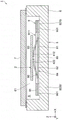
Fig. 1 is an exploded perspective view of a gyro sensor according to a first embodiment, which is an example of an electronic device according to the present invention.
Fig. 2 is a sectional view a-a in fig. 1.
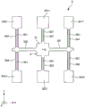
Fig. 3 is a top view (top view) of the gyro sensor shown in fig. 1.
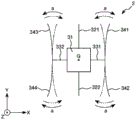
Fig. 4 is a top view (top view) of a gyro element as a functional element.
Fig. 5 is a plan view (top view) showing an electrode arrangement of the gyro element.
Fig. 6 is a plan view (perspective view when viewed from the upper side) showing the arrangement of the electrodes of the gyro element.
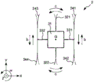
Fig. 7 is a schematic diagram for explaining the operation of the gyro element.
Fig. 8 is a schematic diagram for explaining the operation of the gyro element.
Fig. 9 is a plan view (top view) showing modified example 1 of the support portion.
Fig. 10 is a plan view (top view) showing a modified example 2 of the support portion.
Fig. 11 is a plan view (top view) showing modified example 3 of the support portion.
Fig. 12 is a plan view (top view) showing a modified example 4 of the support portion.
Fig. 13 is a plan view (top view) showing a modified example 5 of the support portion.
Fig. 14 is a plan view (top view) showing a modified example 6 of the support portion.
Fig. 15 is a plan view (top view) showing a modified example 7 of the support portion.
Fig. 16 is a plan view (top view) of the gyro element according to the second embodiment.
Fig. 17 is a plan view (top view) of the gyro element according to the third embodiment.
Fig. 18 is a plan view (top view) of the gyro element according to the fourth embodiment.
Fig. 19 is a plan view (top view) of the gyro element according to the fifth embodiment.
Fig. 20 is a perspective view showing a configuration of a mobile (or notebook) personal computer as an electronic apparatus including the electronic device of the present invention.
Fig. 21 is a perspective view showing the structure of a mobile phone (including PHS) as an electronic device including the electronic apparatus of the present invention.
Fig. 22 is a perspective view showing a configuration of a digital camera as an electronic apparatus including the electronic device of the present invention.
Fig. 23 is a perspective view showing a configuration of a mobile object (automobile) including an electronic device according to the present invention.
Detailed Description
Hereinafter, an electronic device, an electronic apparatus using the electronic device, and a mobile object using the electronic device according to the present invention will be described in detail with reference to preferred embodiments shown in the drawings.
1. Electronic device
First embodiment
First, a structure and a manufacturing method according to a first embodiment of a gyro sensor exemplified as an electronic device of the present invention will be described with reference to fig. 1 to 8. Fig. 1 is an exploded perspective view of a gyro sensor exemplified as an electronic device of the present invention. Fig. 2 shows a cross section of the gyro sensor, and is a cross sectional view a-a in fig. 1. Fig. 3 is a top view (top view) of the gyro sensor shown in fig. 1. In fig. 3, the gyro element is omitted for visual confirmation. Fig. 4 is a top view of the gyroscopic element shown in fig. 1. Fig. 5 is a plan view (top view) showing an electrode arrangement of the gyro element shown in fig. 1. Fig. 6 is a plan view (perspective view when viewed from above) showing an electrode arrangement of the gyro element shown in fig. 1. Fig. 7 and 8 are schematic diagrams for explaining the operation of the gyro element shown in fig. 1.
In addition, hereinafter, for convenience of explanation, in each drawing, an X axis, a Y axis, and a Z axis are illustrated as three axes orthogonal to each other, and a direction parallel to the X axis is referred to as a "first direction or an X axis direction", a direction parallel to the Y axis is referred to as a "second direction or a Y axis direction", and a direction parallel to the Z axis is referred to as a "third direction or a Z axis direction". The + Z axis side is also referred to as "upper", and the-Z axis side is also referred to as "lower".
A gyro sensor (physical quantity sensor) 1, which is an example of the electronic device shown in fig. 1, 2, and 3, includes a gyro element 2 as a functional element for detecting angular velocity, a support portion 9 for supporting the gyro element 2, and a package 5 for housing the gyro element 2 and the support portion 9 so as to be enclosed in one package. The package 5 includes a base (base) 6 and a lid (lid) 7 joined to the base 6, as will be described later. Hereinafter, these respective components will be described in turn.
Gyro element
As shown in fig. 4 to 6, the gyro device 2 as a functional device includes a vibrating reed 3 and an electrode formed on the vibrating reed 3.
Vibrating reed
Examples of the material of the vibrating reed 3 include piezoelectric materials such as crystal, lithium tantalate, and lithium niobate. Among these materials, crystal is preferably used as a structural material of the vibrating piece 3. By using crystal, a gyro element 2 having superior frequency-temperature characteristics compared to other materials can be obtained. Hereinafter, a case where the vibrating piece 3 is made of crystal will be described.
The vibrating reed 3 has a plate shape having a width in an XY plane defined by a Y axis (mechanical axis) and an X axis (electrical axis) which are crystal axes of the crystal substrate, and a thickness in a Z axis (optical axis) direction, and is formed of a so-called Z-cut crystal plate. Although the Z-axis preferably coincides with the thickness direction of the vibrating reed 3, the Z-axis may be slightly (for example, about-5 ° θ 15 °) inclined with respect to the thickness direction from the viewpoint of reducing the frequency temperature change in the vicinity of the normal temperature.
This vibrating reed 3 has: a base 31 located at the center portion; a first detection arm 321 and a second detection arm 322 extending from the base 31 to both sides in the Y-axis direction; a first connecting arm 331 and a second connecting arm 332 extending from the base 31 to both sides in the X-axis direction; a first drive arm 341 and a second drive arm 342 extending from the tip end of the first link arm 331 to both sides in the Y axis direction; a third driving arm 343 and a fourth driving arm 344 extending from the distal end of the second connecting arm 322 to both sides in the Y-axis direction.
The first detection arm 321 extends from the base 31 in the + Y axis direction, and a wide hammer 3211 is provided at a distal end thereof. On the other hand, the second detection arm 322 extends from the base 31 in the-Y axis direction, and a large hammer head 3221 is provided at a tip end portion thereof. The first detection arm 321 and the second detection arm 322 are arranged to be plane-symmetric with respect to an XZ plane passing through the center of gravity G of the gyro element 2. The hammers 3211 and 3221 may be provided as needed or omitted. Further, as necessary, bottomed grooves extending in the longitudinal direction (longitudinal direction) may be formed in the upper and lower surfaces of the first detection arm 321 and the second detection arm 322.
The first link arm 311 extends from the base 31 in the + X axis direction. On the other hand, the second connecting arm 332 extends from the base 31 in the-X axis direction. The first and second link arms 311 and 332 are arranged in plane symmetry with respect to a YZ plane passing through the center of gravity G.
The first driving arm 341 extends in the + Y axis direction from the distal end of the first connecting arm 331, and a large hammer 3411 is provided at the distal end thereof. The second driving arm 342 extends in the-Y axis direction from the distal end of the second connecting arm 331, and a wide hammer 3421 is provided at the distal end thereof. The third driving arm 343 extends in the + Y axis direction from the distal end of the second connecting arm 332, and a large hammer 3431 is provided at the distal end thereof. The fourth drive arm 344 extends in the-Y axis direction from the distal end of the second connecting arm 332, and a large hammer head 3441 is provided at the distal end. The first drive arm 341, the second drive arm 342, the third drive arm 343, and the fourth drive arm 344 are arranged so as to be point-symmetric with respect to the center of gravity G. The hammers 3411, 3421, 3431, 3441 may be provided as needed or omitted.
Further, bottomed grooves 351 extending in the longitudinal direction (longitudinal direction) are formed in the upper and lower surfaces of the first detection arm 321, the second detection portion 322, the first drive arm 341, the second drive arm 342, the third drive arm 343, and the fourth drive arm 344, respectively. Therefore, the cross-sectional shapes of the first detection arm 321, the second detection arm 322, the first drive arm 341, the second drive arm 342, the third drive arm 343, and the fourth drive arm 344 are in the shape of an "H" so as to extend over the entire length in the longitudinal direction of the portion other than the hammer portions ( hammers 3211, 3221, 3411, 3421, 3431, 3441). This narrows the distance between the electrodes formed on the arms in the X-axis direction. Therefore, the efficiency of the electric field between the respective electrodes is improved. As a result, a large amount of charge can be generated with a small amount of deformation in the first detection arm 321, the second detection arm 322, the first drive arm 341, the second drive arm 342, the third drive arm 343, and the fourth drive arm 344. Therefore, the gyro element 2 having excellent sensitivity can be obtained.
Electrode for electrochemical cell
As shown in fig. 5 and 6, the vibrating reed 3 includes, as electrodes: the detection element includes a first detection signal electrode 411, a first detection signal terminal 412, a first detection ground electrode (detection ground electrode) 421, a first detection ground terminal 422, a second detection signal electrode 431, a second detection signal terminal 432, a second detection ground electrode (detection ground electrode) 441, a second detection ground terminal 442, a drive signal electrode 451, a drive signal terminal 452, a drive ground electrode 461, and a drive ground terminal 462. For convenience of explanation, in fig. 5 and 6, the first detection signal electrode 411, the second detection signal electrode 431, the first detection signal terminal 412, the second detection signal terminal 432, the first detection ground terminal 421, the second detection ground electrode 441, the first detection ground terminal 422, the second detection ground terminal 442, the driving signal electrode 451, the driving signal terminal 452, the driving ground electrode 461, and the driving ground terminal 462 are illustrated by different hatching. Further, the electrode formed on the side surface of the vibrating piece 3 is illustrated by a thick line.
The first detection signal electrode 411 is formed on the upper surface and the lower surface (the portion other than the hammer head 3211) of the first detection arm 321, and the second detection signal electrode 431 is formed on the upper surface and the lower surface (the portion other than the hammer head 3221) of the second detection arm 322. The first detection signal electrode 411 and the second detection signal electrode 431 are electrodes for detecting electric charges generated by the vibration when the detection vibration of the first detection arm 331 and the second detection arm 322 is excited.
The first detection signal terminal 412 is provided on the + Y axis side of the row on the + X axis side of the base 31, and is electrically connected to the first detection signal electrode 411 formed on the first detection arm 321 via a wiring not shown. The second detection signal terminal 432 is provided on the-Y axis side of the row on the + X axis side of the base 31, and is electrically connected to the second detection signal electrode 431 formed on the second detection arm 322 via a wiring not shown.
The first detection ground electrode 421 is formed on both side surfaces of the first detection arm 321, and is electrically connected to each other through the hammer head 3211. Similarly, the second detection ground electrode 441 is formed on both side surfaces of the second detection arm 322, and is electrically connected to each other through the hammer head 3221. The first detection ground electrode 421 and the second detection ground electrode 441 have potentials to be grounded with respect to the first detection signal electrode 411 and the second detection signal electrode 431.
The first detection ground terminal 422 is provided on the + Y axis side of the row on the-X axis side of the base 31, and is electrically connected to the first detection ground electrode 421 formed on the first detection arm 321 via a wiring not shown. The second detection ground terminal 442 is provided on the-Y axis side of the row on the-X axis side of the base 31, and is electrically connected to the second detection signal electrode 431 formed on the second detection arm 322 via a wiring not shown.
In this way, by arranging the first detection signal electrode 411 and the second detection signal electrode 431, the first detection signal terminal 412 and the second detection signal terminal 432, the first detection ground electrode 421 and the second detection ground electrode 441, and the first detection ground terminal 422 and the second detection ground terminal 442, it is possible to cause the detection vibration generated in the first detection arm 321 to appear as an electric charge between the first detection signal electrode 411 and the first detection ground electrode 421, and to be extracted as a signal (detection signal) from the first detection signal terminal 412 and the first detection ground terminal 422. Further, the detection vibration generated in the second detection arm 322 can be made to appear as an electric charge between the second detection signal electrode 431 and the second detection ground electrode 441, and can be extracted as a signal (detection signal) from the second detection signal terminal 432 and the second detection ground terminal 442.
The drive signal electrodes 451 are formed on the upper and lower surfaces (portions other than the hammers 3411, 3421) of the first and second drive arms 341, 342. The driving signal electrode 451 is formed on both side surfaces of the third driving arm 343 and the fourth driving arm 344, and is electrically connected to each other through the hammers 3431 and 3441. Such a drive signal electrode 451 is an electrode for exciting the driving vibration of the first drive arm 341, the second drive arm 342, the third drive arm 343, and the fourth drive arm 344.
The drive signal terminal 452 is provided at the center portion of the row on the-X axis side of the base 31 (i.e., between the first detection ground terminal 422 and the second detection ground terminal 442), and is electrically connected to the drive signal electrode 451 formed on the first drive arm 341, the second drive arm 342, the third drive arm 343, and the fourth drive arm 344 via a wiring (not shown).
A driving ground electrode 461 is formed on upper and lower surfaces (portions other than the hammers 3431, 3441) of the third driving arm 343 and the fourth driving arm 344. The driving ground electrodes 461 are formed on both side surfaces of the first driving arm 341 and the second driving arm 342, and are electrically connected to each other through the hammers 3411 and 3421. The driving ground electrode 461 has a potential grounded to the driving signal electrode 451.
The driving ground terminal 462 is provided at the center portion of the row on the + X axis side of the base 31 (i.e., between the first detection signal terminal 412 and the second detection signal terminal 432), and is electrically connected to a driving ground electrode 461 formed on the first driving arm 341, the second driving arm 342, the third driving arm 343, and the fourth driving arm 344 through a wiring (not shown).
In this way, by arranging the driving signal electrode 451, the driving signal terminal 452, the driving ground electrode 461, and the driving ground terminal 462 and applying the driving signal between the driving signal terminal 452 and the driving ground terminal 462, an electric field can be generated between the driving signal electrode 451 and the driving ground electrode 461 formed on the first driving arm 341, the second driving arm 342, the third driving arm 343, and the fourth driving arm 344, and the first driving arm 341, the second driving arm 342, the third driving arm 343, and the fourth driving arm 344 can be driven and vibrated, respectively.
The electrode may be configured by, for example, a metal film in which films of Ni (nickel), Au (gold), Ag (silver), Cu (copper), and the like are laminated on a metallization layer (underlying layer) of Cr (chromium), W (tungsten), and the like.
The metal films formed on the hammers 3211 and 3221 function as an adjustment film for adjusting the frequency of the detection vibration mode, and for example, the mass of the first detection arm 321 and the second detection arm 322 can be adjusted by removing a part of the metal films by laser irradiation or the like to adjust the frequency of the detection vibration mode. On the other hand, the metal films formed on the hammers 3411, 3421, 3431, and 3441 function as an adjustment film for adjusting the frequency of the driving vibration mode, and for example, the mass of the first detection arm 321, the second detection arm 322, the third drive arm 343, and the fourth drive arm 344 can be adjusted by removing a part of the metal film by laser irradiation or the like, thereby adjusting the frequency of the driving vibration mode.
The structure of the gyro element 2 is briefly described above. Next, the driving of the gyro element 2 will be briefly described with reference to fig. 7 and 8.
When a voltage (ac voltage) is applied between the drive signal terminal 452 and the drive ground terminal 462 in a state where no angular velocity is applied to the gyro element 2, an electric field is generated between the drive signal electrode 451 and the drive ground electrode 461, and the respective drive arms 341, 342, 343, 344 are caused to perform buckling vibration in the direction indicated by arrow a as shown in fig. 7. At this time, since the first and second driving arms 341 and 342 and the third and fourth driving arms 343 and 344 perform vibrations symmetrical with respect to the YZ plane passing through the center of gravity G of the gyro element 2, the base 31, the first and second detection arms 321 and 322, the first and second connection arms 331 and 332 hardly vibrate.
In a state where such driving vibration is carried out, when an angular velocity ω about the Z axis is applied to the gyro element 2, the detection vibration shown in fig. 8 is excited. Specifically, coriolis force in the direction indicated by arrow b acts on each of the drive arms 341, 342, 343, and 344 and the first and second connecting arms 331 and 332, and new vibration is excited. The vibration in the direction of arrow "b" is a vibration in the circumferential direction with respect to the center of gravity "G". At the same time, detection vibration in the direction of arrow mark c is excited in first detection arm 321 and second detection arm 322 in response to vibration of arrow mark b. The electric charges generated in the first detection arm 321 and the second detection arm 322 by the vibration are extracted as signals from the first detection signal electrode 411 and the second detection signal electrode 431 and the first detection ground electrode 421 and the second detection ground electrode 441, and the angular velocity ω is obtained from the signals.
Support part
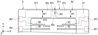
Next, returning to fig. 1 to 3, the structure of the support portion 9 will be described. The support portion 9 is a light-transmissive substrate for TAB (Tape Automated Bonding) mounting, which is conventionally known, and supports the gyro element 2. The support portion 9 includes a frame-shaped base material (support substrate) 91, six support leads 92, 93, 94, 95, 96, 97 (also referred to as bonding leads (wires)) provided on the base material 91, and shield portions 8a, 8b as conductive patterns.
The base 91 serving as a support substrate is made of a flexible resin such as polyimide, for example. The base 91 has a substantially rectangular frame shape having an opening 910 at the center, and is disposed in the recess 61 so that the major axis thereof coincides with the major axis of the package 5. The base material 91 includes two intermediate portions 911 and 912 facing each other along the longitudinal direction (X-axis direction in the drawing) of the base material 91.
The six support leads 92 to 97 are bonding leads (wires) for supporting the gyro element 2, and are wiring patterns formed by conductive members having conductivity. In the present embodiment, a metal material such as copper (Cu) or a copper alloy is used as the conductive member. Six support leads 92 to 97 are fixed to the lower surface of the base member 91. The support leads 92, 93, and 94 are disposed on the right side (one side in the X-axis direction as the long axis direction) of the base 91 in fig. 3, and the distal ends thereof extend into the opening 910 of the base 91. On the other hand, the support leads 95, 96, 97 are disposed in a left side portion (the other side in the X-axis direction as the long axis direction) of the base member 91 in fig. 3, and distal end portions thereof extend into the opening 910 of the base member 91. The distal ends of the support wires 92, 93, and 94 are separated from and opposed to the distal ends of the support wires 95, 96, and 97 at the center of the opening 910.
The support leads 92 to 97 are inclined at the middle, and the tip ends thereof are positioned above the base material 91 (+ Z-axis direction). The support wires 92 to 97 are narrowed in width at the middle, and the distal end portion is thinner than the proximal end portion. The distal end portions of the support wires 92 to 97 are disposed so as to correspond to (overlap with) the first detection signal terminal 412, the first detection ground terminal 422, the second detection signal terminal 432, the second detection ground terminal 442, the drive signal terminal 452, and the drive ground terminal 462 of the gyro element 2.
The base end portions of the support wires 92 and 95 serve as connection terminals 921 and 951, and the support wires 92 and 95 extend straight from the connection terminals 921 and 951. On the other hand, the base end portions of the support leads 93, 94, 96, 97 serve as connection terminals 931, 941, 961, 971, and the support leads 93, 94, 96, 97 extend while being bent at right angles from the connection terminals 931, 941, 961, 971 toward the support leads 92, 95.
The connection terminals 921 and 951 and the connection terminals 931, 941, 961, and 971 are mounting portions (connection portions) that correspond to and are connected to an S1 connection terminal 801b, an S2 connection terminal 802b, GND connection terminals 803 b', 803b ″, a DS connection terminal 804b, and a DG connection terminal 805b provided on the upper surface of the base 6 of the package 5 described later. Specifically, the mounting part has a first mounting part including connection terminals 921, 931, 941 located on the right side (+ X-axis direction) in fig. 3 and a first mounting part including connection terminals 951, 961, 971 located on the left side (-X-axis direction) in fig. 3. The first mounting portion and the second mounting portion are connected by an intermediate portion 911 and an intermediate portion 912.
The shield portions 8a and 8b as conductive patterns extend from the connection terminal 961 and the connection terminal 971. The shield portions 8a and 8b are thin plate-like conductive patterns made of conductive members having conductivity, similarly to the connection terminal 961 and the connection terminal 971. In the present embodiment, a metal material made of copper (Cu), a copper alloy, or the like, for example, is used as the conductive member. The shield portions 8a and 8b are laminated (fixed) on the lower surfaces of intermediate portions 911 and 912 located on both sides in the Y-axis direction between the first mounting portion and the second mounting portion in the frame-shaped base member 91 constituting the support portion 9. In addition to the above, for example, carbon materials can be used as the components of the shields 8a and 8 b.
Specifically, the shield portion 8a extends from the connection terminal 961 so as to substantially follow the planar shape of the intermediate portion 911, and is laminated (fixed) on the back surface of the intermediate portion 911. The shield part 8a includes a first wide large part 81 and a second wide large part 82, which are wide large parts, of a width W1, and a narrow part 87 having a width W2 between the first wide large part 81 and the second wide large part 82, where the width W1 is a width dimension (dimension in the Y axis direction) substantially equal to the width of the intermediate part 911 (distance between the outer edge 811 and the inner edge 813), and the width W2 is a width (distance between the bottom of the recess 85 and the inner peripheral edge 813) narrowed by the recess 85, which is a slit part cut into the shield part 8a from the outer edge 811. In other words, the wide portion includes a first wide portion 81 provided on one side in the first direction (X-axis direction) via the narrow portion 87, and a second wide portion 82 provided on the other side.
Here, the connection terminal 961 and the connection terminal 971, on which the shielding portions 8a and 8b are extended, correspond to the GND connection terminals 803' and 803 ″ provided on the upper surface of the base 6 of the package 5. That is, the shields 8a and 8b are fixed potentials connected to GND. In this way, by setting the shielding portions 8a and 8b to a fixed potential, it is possible to effectively shield (shield) the electric noise emitted from, for example, a high-frequency signal wiring through which a high-frequency signal flows, a digital signal wiring through which a digital signal flows, and the like, to the first detection signal electrode 411 and the second detection signal electrode 431, which are the detection electrodes of the vibrating reed 3. The shielding portions 8a and 8b do not necessarily have to be a fixed potential connected to GND, and may be a fixed potential electrically connected to a fixed potential source held at the fixed potential, whereby the shielding effect can be obtained.
The shield portion 8b extends from the connection terminal 971 so as to substantially follow the planar shape of the intermediate portion 912, and is fixed to the rear surface of the intermediate portion 912. The shield 8b includes a first wide portion 83 and a second wide portion 84, which are wide portions, of a width W1, and a narrow portion 88 of a width W2 (a width in the Y-axis direction) between the first wide portion 83 and the second wide portion 84, where the width W1 is substantially the same width (a width in the Y-axis direction) as a width of the intermediate portion 912 (a distance between the outer edge 812 and the inner edge 814), and the width W2 is a width (a distance between the bottom of the concave portion 86 and the inner edge 814) narrowed by the concave portion 86, which is a slit portion that is recessed from the outer edge 812 of the shield 8 b. In other words, the wide portion includes a first wide portion 83 provided on one side in the first direction (X-axis direction) via the narrow portion 88, and a second wide portion 84 provided on the other side.
In this way, since the first wide portions 81 and 83 and the second wide portions 82 and 84 are provided on both sides of the narrow portions 87 and 88, it is possible to absorb stress due to expansion and contraction caused by thermal changes and the like occurring in the first wide portions 81 and 83 and the second wide portions 82 and 84 by the narrow portions 87 and 88 smoothly and efficiently. This effectively suppresses a decrease in the connection strength between the connection terminals 951, 961, and 971 (second mounting portions) and the connection terminals 921, 931, and 941 (first mounting portions), which are mounting portions between the base 6 and the support portion 9, due to the stress.
In addition, it is preferable that the shielding portions 8a and 8b are disposed so as to overlap at least a part of the first detection signal electrode 411 and the second detection signal electrode 431 (see fig. 5) as the detection electrodes provided in the gyro element when the gyro element 2 is viewed from above in the drawing in a plan view. In this way, by disposing the shielding portions 8a and 8b, it is possible to shield (shield) the electric noise (radiation noise) that affects the detection value relating to the physical quantity detected by the first detection signal electrode 411 and the second detection signal electrode 431 as the detection electrodes, thereby reducing the effect.
As described above, the support portion 9 includes: a frame-shaped base material 91; support leads 92, 93, 94 and support leads 95, 96, 97 each having three sections fixed to a frame portion of the base 91 facing the X axis direction in the drawing; the portions are fixed to the shield portions 8a and 8b at the intermediate portions 911 and 912 of the frame portion facing in the Y axis direction in the figure as the base 91. In other words, the support portion 9 includes connection terminals 921, 931, and 941 as first mounting portions and connection terminals 951, 961, and 971 as second mounting portions, which are provided separately in the X-axis direction as the first direction with the intermediate portions 911 and 912 of the shield portions 8a and 8b fixed to the respective lower surfaces thereof interposed therebetween. The support portion 9 is attached to the base 6 of the package 5 described later at portions of the connection terminals 921, 931, and 941 as the first attachment portions and the connection terminals 951, 961, and 971 as the second attachment portions.
Package member
The package 5 includes a box-shaped base (base) 6 and a plate-shaped cover (lid) 7, the base 6 has a recess 61 opened in an upper surface, and the cover 7 is coupled to the base 6 so as to close the opening of the recess 61. Further, the gyro element 2 described above is accommodated in the internal space S formed by closing the opening of the recess 61 with the lid 7. Although the environment of the internal space S is not particularly limited, in the present embodiment, a vacuum state (for example, a reduced pressure state of 10Pa or less) is assumed.
The base 6 has a substantially rectangular (rectangular) outer shape in plan view, and has a pair of outer edges extending in the major axis direction and a pair of outer edges extending in the minor axis direction (direction intersecting the major axis). However, the shape of the base 6 in plan view is not limited to a rectangle, and may be, for example, a square, a polygon having a pentagon or more, or a special shape. As a material constituting the base 6, ceramics or the like can be preferably used. As another material constituting the base 6, for example, a Printed Circuit Board (PCB) having a resin substrate such as an epoxy substrate as a base can be used.
On the upper surface (bottom surface of the recess 61) of the base 6, an S1 connection terminal 801b, an S2 connection terminal 802b, GND connection terminals 803', 803 ″, a DS connection terminal 804b, and a DG connection terminal 805b are provided so as to be separated from each other. These S1 connection terminals 801b, S2 connection terminals 802b, GND connection terminals 803', 803 ″, DS connection terminals 804b, and DG connection terminals 805b are provided so as to correspond to (overlap) the connection terminals 921 to 941 and the connection terminals 951 to 971 of the support leads 92 to 94 and the support leads 95 to 97, respectively, and are joined to each other when the support portion 9 is housed in the package 5.
The S1 connection terminal 801b is joined to the connection terminal 931, and the S2 connection terminal 802b is joined to the connection terminal 941. GNP connection terminal 803' is joined to connection terminal 961, and GNP connection terminal 803 ″ is joined to connection terminal 971. The DS connection terminal 804b is joined to the connection terminal 951, and the DG connection terminal 805b is joined to the connection terminal 921.
Further, through electrodes (not shown) are formed on the base 6 at portions corresponding to the respective connection terminals 801b, 802b, 803 b', 803 ", 804b, 805b, and are connected to external terminals (not shown) provided on the lower surface of the base 6. This enables the electrode of the gyro element 2 to be electrically connected to the outside.
Base material (support substrate) 91 constituting support part 9, and shield parts 8a, 8b fixed to base material 91, support leads 92 to 97, and heat of ceramics constituting package 5The expansion coefficients (linear expansion coefficients) are different. The typical thermal expansion coefficient (linear expansion coefficient) of the polyimide resin (polyimide film) constituting the base material 91 is, for example, 27 × 10-6The coefficient of thermal expansion (linear expansion coefficient) of copper (Cu) constituting the shield parts 8a, 8b and the support leads 92 to 97 is, for example, 16.8X 10 DEG C-6The typical coefficient of thermal expansion (linear expansion coefficient) of the ceramic constituting the package 5 is, for example, 7.1 × 10 ° c-6/℃。
Here, the polyimide resin (polyimide film) constituting the substrate 91 is a flexible substrate and easily absorbs stress generated by expansion and contraction due to a change in environmental temperature. In contrast, the copper (Cu) constituting the shield parts 8a and 8b and the support leads 92 to 97 and the ceramic constituting the package 5 have high rigidity, and are less likely to absorb stress generated by expansion and contraction due to a change in environmental temperature, and are more likely to be affected by the stress.
In particular, like the present embodiment, in the structure in which the package 5 and the support portion 9 are mounted at both sides of the connection terminals 921, 931, 941 as the first mounting portions and the connection terminals 951, 961, 971 as the second mounting portions, stress between the connection terminals 921, 931, 941 and the connection terminals 951, 961, 971, which is expanded and contracted by a change in the environmental temperature, is concentrated at the connection portions.
In contrast, in the gyro sensor 1 of the present embodiment, the narrow portions 87 and 88 are provided in the shield portions 81 and 8b at positions between the connection terminals 921, 931, and 941 and the connection terminals 951, 961, and 971. Since the narrowed portions 87 and 88 narrow the width dimension (width W2), the rigidity is weakened, and the stress generated by the difference in the amount of expansion and contraction of each member due to the change in the ambient temperature can be absorbed. Thereby, a decrease in the connection strength of the package 5 (the base 6) and the mounting portions of the support portion 9 (the connection terminals 921, 931, 941 as the first mounting portions and the connection terminals 951, 961, 971 as the second mounting portions) can be suppressed, and the gyro sensor 1 having improved connection reliability can be provided.
Modification examples
Next, a modified example of the support portion 9 of the gyro sensor 1 according to embodiment 1 described above will be described with reference to fig. 9 to 15. Here, fig. 9 to 14 are plan views (top views) showing modified examples 1 to 6 of the support portion, fig. 9 shows modified example 1, fig. 10 shows modified example 2, fig. 11 shows modified example 3, fig. 12 shows modified example 4, fig. 13 shows modified example 5, and fig. 14 shows modified example 6. Fig. 9 to 14 show a partial plan view of the support portion 9, and have the same configuration on the opposite side with respect to the support wires 92, 93, 94, 95, 96, and 97. Fig. 15 is a plan view (top view) showing a modified example 7 of the support portion. In the following description, the same components as those of the first embodiment described above are denoted by the same reference numerals, and description thereof may be omitted or simplified.
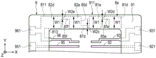
First, modified example 1 of the support portion 9 will be described with reference to fig. 9. As shown in fig. 9, the supporting portion 9 according to modified example 1 also includes a frame-shaped base member (supporting board) 91, six supporting leads 92, 93, 94, 95, 96, 97 (the supporting leads 94, 97 are not shown) provided on the base member 91, and a shield portion 8c, as in the first embodiment.
The shield portion 8c extends from the connection terminal 961. The shield portion 8c is laminated (fixed) on the lower surface of the intermediate portion 911 located on both sides in the Y-axis direction between the first mounting portion and the second mounting portion in the frame-shaped base member 91. The shield portion 8c extends from the connection terminal 961 so as to substantially follow the planar shape of the extended intermediate portion 911.
The shield portion 8c has three wide large portions (a first wide large portion 81a, a second wide portion 82a, and a third wide portion 89a) having a width W1 substantially equal to the width of the intermediate portion 911 (the dimension in the Y-axis direction), and two narrow portions (a first narrow portion 87a and a second narrow portion 87b) sandwiched by the wide portions.
The narrow portion includes a first narrow portion 87a located between the first broad portion 81a and the third broad portion 89a and a second narrow portion 87b located between the second broad portion 82a and the third broad portion 89 a. The first narrow portion 87a has a width W2a whose width dimension (dimension in the Y-axis direction) is narrowed by the recess portion 85a as a narrow portion cut from the outer edge 811 of the shield portion 8 c. The second narrow portion 87b has a width W2b whose width dimension (dimension in the Y-axis direction) is narrowed by the recess 85b as a narrow portion cut from the outer edge 811 of the shield portion 8 c. The width W2a of the first narrow part 87a may be the same as or different from the width W2 8926 of the second narrow part 87bW2 b.
Modification example 2 of support part
First, a modified example 2 of the support portion 9 will be described with reference to fig. 10. As shown in fig. 10, the supporting portion 9 according to the modified example 2 also includes a frame-shaped base material (supporting board) 91, six supporting leads 92, 93, 94, 95, 96, 97 (the supporting leads 94, 97 are not shown) provided on the base material 91, and a shield portion 8d, as in the first embodiment.
The shield portion 8d extends from the connection terminal 961. The shield portion 8d is laminated (fixed) on the lower surface of the intermediate portion 911 located on both sides in the Y-axis direction between the first mounting portion and the second mounting portion in the frame-shaped base member 91. The shield portion 8d extends from the connection terminal 961 so as to substantially follow the planar shape of the extended intermediate portion 911.
The shield portion 8d has two wide large portions (a first wide large portion 81c and a second wide large portion 82c) having a width W1 substantially equal to the width of the intermediate portion 911 (the dimension in the Y axis direction), and a narrow portion 87c having a width W2 narrowed by a recess portion 85c serving as a slit portion cut from the inner peripheral edge 813 of the shield portion 8d and sandwiched between the first wide large portion 81c and the second wide portion 82 c. As in the present modification, the same effects as those of the first embodiment are obtained also in the configuration in which the narrowed portion 87c of the width W2 whose width dimension (dimension in the Y-axis direction) is narrowed is provided on the outer edge 811 side of the shield portion 8 d.
Modification example 3 of support part
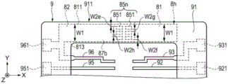
First, a modified example 3 of the support portion 9 will be described with reference to fig. 11. As shown in fig. 11, the supporting portion 9 according to modification 3 also includes a frame-shaped base member (supporting board) 91, six supporting leads 92, 93, 94, 95, 96, 97 (the supporting leads 94, 97 are not shown) provided on the base member 91, and a shield portion 8e, as in the first embodiment.
The shield portion 8e extends from the connection terminal 961. The shield portion 8e is laminated (fixed) on the lower surface of the intermediate portion 911 located on both sides in the Y-axis direction between the first mounting portion and the second mounting portion in the frame-shaped base member 91. The shield portion 8e extends from the connection terminal 961 so as to substantially follow the planar shape of the extended intermediate portion 911.
The shield portion 8e has four wide large portions (a first wide large portion 81d, a second wide portion 82d, a third wide portion 81e, and a fourth wide portion 82e) having a width W1 substantially equal to the width of the intermediate portion 911 (the dimension in the Y axis direction), and three narrow portions (a first narrow portion 87e, a second narrow portion 87d, and a third narrow portion 87f) sandwiched by the wide portions.
The narrow portion includes a first narrow portion 87e between the first wide portion 81d and the third wide portion 89e, a second narrow portion 87d between the third wide portion 81e and the fourth wide portion 82e, and a third narrow portion 87f between the fourth wide portion 81e and the second wide portion 82 d.
The first narrow portion 87e has a width W2d whose width dimension (dimension in the Y axis direction) is narrowed by a recess 85e as a narrow portion cut from the inner peripheral edge 813 of the shield portion 8 e. Similarly, the third narrow portion 87f has a width W2e in which the width dimension (dimension in the Y-axis direction) is narrowed by the recess portion 85f as a narrow portion cut from the inner peripheral edge 813 of the shield portion 8 e. The second narrow portion 87d has a width W2c whose width dimension (dimension in the Y-axis direction) is narrowed by a recess 85d, which is a narrow portion, cut from the outer edge 811 of the shield portion 8 e. In this way, the same effects as those of the first embodiment are obtained also in the configuration in which the cut-in side of the recess of the narrowed portion 8e is the inner peripheral edge 813 side of the shield portion 8e or the outer edge 811 side of the shield portion 8 e.
The direction of cutting or the arrangement of the cutting direction is not limited. The width W2d of the first narrow portion 87e, the width W2c of the second narrow portion 87d, and the width W2e of the third narrow portion 87f may be the same or different.
Modification example 4 of support part
First, a modified example 4 of the support portion 9 will be described with reference to fig. 12. As shown in fig. 12, the support portion 9 according to modification 4 also includes a frame-shaped base member (support substrate) 91, six support leads 92, 93, 94, 95, 96, 97 (the support leads 94, 97 are not shown) provided on the base member 91, and a shield portion 8f, as in the first embodiment.
The shield portion 8f extends from the connection terminal 961. The shield portion 8f is laminated (fixed) on the lower surface of the intermediate portion 911 located on both sides in the Y-axis direction between the first mounting portion and the second mounting portion in the frame-shaped base member 91. The shield portion 8f extends from the connection terminal 961 so as to substantially follow the planar shape of the extended intermediate portion 911.
The shield portion 8f has two wide large portions (a first wide large portion 81 and a second wide large portion 82) having a width W1 substantially equal to the width of the intermediate portion 911 (the dimension in the Y axis direction), and a narrow portion 87g sandwiched between the first wide large portion 81 and the second wide large portion 82.
The narrow portion 87g has a width W2 whose width dimension (dimension in the Y axis direction) is narrowed by a recess 85g as a slit portion cut from an outer edge 811 of the shield portion 8f and a recess 85h as a slit portion cut from an inner edge 813 of the shield portion 8 f. In this way, the same effect as that of the first embodiment can be obtained also in a configuration in which the direction of forming the recess forming the narrowed portion is cut in a different direction, such as the inner peripheral edge 813 side of the shield portion 8f or the outer edge 811 side of the shield portion 8 e. The cutting dimension (depth of the recess) into which the outer edge 811 of the recess 85g is cut and the cutting dimension (depth of the recess) into which the inner edge 813 of the recess 85h is cut are not limited, and may be the same or different. Further, the size of the width W2 is not limited.
Modification example 5 of support part
First, a modified example 5 of the support portion 9 will be described with reference to fig. 13. As shown in fig. 13, the supporting portion 9 according to modification example 5 also includes a frame-shaped base member (supporting board) 91, six supporting leads 92, 93, 94, 95, 96, 97 (the supporting leads 94, 97 are not shown) provided on the base member 91, and a shield portion 8g, as in the first embodiment.
The shield portion 8g extends from the connection terminal 961. The shield portion 8g is laminated (fixed) on the lower surface of the intermediate portion 911 located on both sides in the Y-axis direction between the first mounting portion and the second mounting portion in the frame-shaped base member 91. The shield portion 8d extends from the connection terminal 961 so as to substantially follow the planar shape of the extended intermediate portion 911.
The shield 8g has two wide large portions (a first wide large portion 81 and a second wide portion 82) having a width W1 substantially equal to the width of the intermediate portion 911 (the dimension in the Y axis direction), and a first narrow portion 87k and a second narrow portion 87j constituting narrow portions sandwiched between the first wide portion 81 and the second wide portion 82.
The first narrow portion 87k and the second narrow portion 87j are formed by a substantially rectangular through-hole 85k provided in the intermediate portion 911 of the shielding portion 8g 1. The first narrow portion 87k is configured to have a width W2d between the through hole 85k and the inner peripheral edge 811 of the shield portion 8g, and the second narrow portion 87j is configured to have a width W2c between the through hole 85k and the outer edge 813 of the shield portion 8 g. In this way, even if the narrow portion is configured by providing the through hole 85k, for example, the same effect as that of the first embodiment is obtained.
A plurality of through holes 85k may be provided, and as shown by the imaginary line (two-dot chain line) in the figure, for example, a configuration in which two through holes 85m are added and three through holes are provided may be adopted. The shape of the through-hole 85k is not limited to a rectangular shape, and may be other shapes such as a circular shape, an elliptical shape, and a polygonal shape. The width W2d of the first narrow portion 87k and the width W2c of the second narrow portion 87j may be the same or different.
Modification example 6 of support part
First, a modified example 6 of the support portion 9 will be described with reference to fig. 14. As shown in fig. 14, the supporting portion 9 according to modification example 6 also includes a frame-shaped base member (supporting board) 91, six supporting leads 92, 93, 94, 95, 96, 97 (the supporting leads 94, 97 are not shown) provided on the base member 91, and a shield portion 8h, as in the first embodiment.
The shield portion 8h extends from the connection terminal 961. The shield portion 8h is laminated (fixed) on the lower surface of the intermediate portion 911 located on both sides in the Y-axis direction between the first mounting portion and the second mounting portion in the frame-shaped base member 91. The shield portion 8h extends from the connection terminal 961 so as to substantially follow the planar shape of the extended intermediate portion 911.
The shield portion 8h has two wide large portions (a first wide large portion 81 and a second wide large portion 82) having a width W1 substantially equal to the width of the intermediate portion 911 (the dimension in the Y axis direction), and a narrow portion 85n sandwiched between the first wide large portion 81 and the second wide large portion 82.
The narrowing portion 85n is configured by aligning a plurality of through holes 851. Specifically, three through-holes 851 are arranged in line with each other in the width direction (Y-axis direction) of the shield portion 8h so as to have widths W2g and W2 h. At this time, the narrow portion is arranged to have a width W2f as a space between the inner peripheral edge 813 and the inner through-hole 851 and a width W2e as a space between the outer edge 811 and the outer through-hole 851. In this example, a structure in which the columns are arranged in two columns is adopted. The number, shape, arrangement pattern, and the like of the through holes 851 are not limited. In this way, even if the narrow portion 85n is configured by the plurality of through holes 851, the same effect as that of the first embodiment is obtained.
Modified example 7 of support part
First, a modified example 7 of the support portion 9 will be described with reference to fig. 15. As shown in fig. 15, the supporting portion 9 according to the modified example 7 also includes a frame-shaped base material (supporting board) 91, six supporting lead wires 92, 93, 94, 95, 96, 97 provided on the base material 91, and shield portions 8a, 8b, as in the first embodiment.
The shield portion 8a extends from the connection terminal 961. Further, the shield portion 8b extends from the connection terminal 971. The shield portions 8a and 8b are laminated (fixed) on the lower surfaces of the intermediate portions 911 and 912 located on both sides in the Y-axis direction between the first mounting portion and the second mounting portion in the frame-shaped base member 91. The shield portions 8a and 8b extend from the connection terminals 961 and 971 to substantially follow the planar shape of the extending intermediate portions 911 and 912.
The shield portion 8a has three wide large portions (a first wide large portion 81a, a second wide portion 82a, and a third wide portion 89a) having a width W1 substantially equal to the width of the intermediate portion 911 (the dimension in the Y-axis direction), and two narrow portions (a first narrow portion 87a and a second narrow portion 87b) sandwiched by the wide portions.
The narrow portion includes a first narrow portion 87a located between the first broad portion 81a and the third broad portion 89a and a second narrow portion 87b located between the second broad portion 82a and the third broad portion 89 a. The first narrow portion 87a has a width W2 whose width dimension (dimension in the Y axis direction) is narrowed by a recess 85a as a narrow portion cut from an outer edge 811 of the shield portion 8 a. The first narrow portion 87b has a width W2 whose width dimension (dimension in the Y-axis direction) is narrowed by a recess 85b as a narrow portion cut from the outer edge 811 of the shield portion 8 a. The width W2 of the first narrow part 87a may be the same as or different from the width W2 of the second narrow part 87 b.
The shield portion 8b has two wide large portions (a first wide large portion 83 and a second wide portion 84) having a width W1 substantially equal to the width of the intermediate portion 912 (the dimension in the Y-axis direction), and a narrow portion 88 sandwiched between the first wide large portion 83 and the second wide portion 84. The narrow portion 88 has a width W2 whose width dimension (dimension in the Y axis direction) is narrowed by the recess 86 as a slit portion cut from the outer edge 812 of the shield portion 8 b.
According to modification 7, the shield portion 8a and the shield portion 8b are configured to have different arrangements of the wide portion and the narrow portion. This configuration also provides the same effects as those of the first embodiment.
According to the gyro sensor 1 including the modifications 1 to 7 of the support portion 9 described above, the same effects as those of the gyro sensor 1 of the first embodiment can be obtained. That is, the shield portions 8c, 8d, 8e, 8f, 8g, 8h, 8a, and 8b are provided with the narrow portions 87a, 87b, 87c, 87d, 87e, 87f, 87g, 87k, 85n, and 88 having a narrow width dimension, respectively, to reduce the rigidity, thereby improving the effect of absorbing the stress caused by the difference in the amount of expansion and contraction of the respective members due to the change in the ambient temperature. This can suppress a decrease in the connection strength between the package 5 (base 6) and the mounting portion of the support portion 9 (the connection terminals 921, 931, and 941 as the first mounting portions and the connection terminals 951, 961, and 971 (see fig. 3) as the second mounting portions), and can improve the connection reliability of the gyro sensor 1.
Second embodiment
Next, a configuration according to a second embodiment of a gyro sensor exemplified as an electronic device of the present invention will be described with reference to fig. 16. Fig. 16 is a plan view (top view) of a gyro element according to a second embodiment illustrated as an electronic device of the present invention. Hereinafter, a second embodiment of the gyro element exemplified as the electronic device of the present invention will be described, but differences from the above-described embodiments will be mainly described, and the same configurations and matters will be denoted by the same reference numerals or description thereof will be omitted. In the second embodiment, the configuration is substantially the same as that of the first embodiment described above except that the configuration of the intermediate portion of the support portion is different.
A gyro sensor 10 according to a second embodiment shown in fig. 16 includes a gyro element 2 (see fig. 1) as a functional element for detecting angular velocity, a support portion 9 for supporting the gyro element 2, and a package 5 for containing the gyro element 2 and the support portion 9 in one package, as in the first embodiment. The package 5 includes a base 6 and a lid 7 (see fig. 2) joined to the base 6, although the description will be given later. Hereinafter, a description will be given mainly on a structure relating to an intermediate portion of a support portion different from that of the first embodiment.
The support portion 9 according to the second embodiment also includes a frame-shaped base material (support substrate) 91, six support leads 92, 93, 94, 95, 96, and 97 provided on the base material 91, and shield portions 8a and 8b, as in the first embodiment. The support portion 9 is also a light-transmissive substrate for TAB mounting, and supports the gyro element 2, as in the first embodiment.
The base 91 serving as a support substrate is made of a flexible resin such as polyimide. The base 91 has a substantially rectangular frame shape having an opening 910 at the center, and is disposed in the recess 61 so that the major axis thereof coincides with the major axis of the package 5. The base material 91 includes two intermediate portions 911 and 912 facing each other along the longitudinal direction (X-axis direction in the drawing) of the base material 91.
The shield portions 8a and 8b are also thin plate-like conductive patterns made of a metal material, and are made of, for example, copper (Cu) or a copper alloy, as in the case of the connection terminal 961 and the connection terminal 971 of the support leads 96 and 97. The shield portion 8a extends from the connection terminal 961. Further, the shield portion 8b extends from the connection terminal 971. The shield portions 8a and 8b are laminated (fixed) on the lower surfaces of the intermediate portions 911 and 912 located on both sides in the Y axis direction between the first mounting portion (the portion where the connection terminals 921, 931, and 941 are located) and the second mounting portion (the portion where the connection terminals 951, 961, and 971 are located) in the X axis direction in the frame-shaped base material 91. The shield portions 8a and 8b extend from the connection terminals 961 and 971 to substantially follow the planar shape of the extending intermediate portions 911 and 912.
Specifically, the shield portion 8a extends from the connection terminal 961 so as to substantially follow the planar shape of the intermediate portion 911, and is laminated (fixed) on the back surface of the intermediate portion 911. The shield part 8a includes a first wide large part 81 and a second wide large part 82, which are wide large parts, of a width W1, and a narrow part 87 of a width W2 located between the first wide large part 81 and the second wide large part 82, wherein the width W1 is a width (dimension in the Y axis direction) substantially equal to the width of the intermediate part 911, and the width W2 is a width in which the width (dimension in the Y axis direction) is narrowed by a concave part 85, which is a slit part cut from an outer edge 811 of the shield part 8 a. In other words, the wide portion includes a first wide portion 81 provided on one side in the first direction (X-axis direction) and a second wide portion 82 provided on the other side with the narrow portion 87 interposed therebetween.
Further, a second recess 70 as a slit portion into which a resin such as polyimide is cut from the outer peripheral edge is provided in the intermediate portion 911 of the base material 91 facing the recess 85 of the shield 8 a. That is, the concave portion 85 of the shield portion 8a and the second concave portion 70 of the intermediate portion 911 cut into resin such as polyimide are arranged so as to overlap with each other in a plan view seen in the Z-axis direction in the drawing.
The shield portion 8b extends from the connection terminal 971 so as to substantially follow the planar shape of the intermediate portion 912, and is laminated (fixed) on the rear surface of the intermediate portion 912. The shield 8b includes a first wide portion 83 and a second wide portion 84, which are wide portions, having a width W1 (width W1 is substantially the same width (dimension in the Y-axis direction) as the width of the intermediate portion 912, and a narrow portion 88 having a width W2 (dimension in the Y-axis direction) narrowed by a recess 86, the recess 86 being located between the first wide portion 83 and the second wide portion 84 and being a slit portion recessed from the outer edge 812 of the shield 8 b. In other words, the wide portion includes a first wide portion 83 provided on one side in the first direction (X-axis direction) with the narrow portion 88 interposed therebetween, and a second wide portion 84 provided on the other side.
Further, a second recess 71 as a slit portion into which a resin such as polyimide is cut from the outer peripheral edge is provided in the intermediate portion 912 of the base member 91 facing the recess 86 of the shield 8 b. That is, the concave portion 86 of the shield portion 8b and the second concave portion 71 of the intermediate portion 912, which is cut into resin such as polyimide, are arranged so as to overlap each other when viewed from the Z-axis direction in the drawing in a plan view.
According to this configuration, the rigidity of the shields 81a and 8b is weakened by the narrow portions 87 and 88 provided between the connection terminals 921, 931, and 941 and the connection terminals 951, 961, and 971, and stress generated by a difference in expansion and contraction amounts of the respective members due to a change in ambient temperature can be absorbed. In addition, by arranging the second concave portions 70 and 71 as slit portions on the intermediate portions 911 and 912 of the base material 91 (support portion 9) so as to overlap the concave portions 85 and 86 of the shield portions 8a and 8b when viewed in a plan view in the Z-axis direction in the drawing, it is possible to reduce stress generated in the first and second mounting portions due to a difference in the amount of expansion or contraction caused by a difference in the thermal expansion coefficient between the base material 91 as a support substrate and the base 6 when the ambient temperature changes. Therefore, a decrease in the connection strength of the mounting portions (the first mounting portion and the second mounting portion) of the base and the support portion including the connection terminals 921, 931, 941 and the connection terminals 951, 961, 971 can be suppressed, and connection reliability can be improved.
In addition to the second concave portion 70 provided at a position overlapping with the concave portion 85, as shown by a virtual line (one-dot chain line) in fig. 16, the second concave portions 70a, 70b and the like may be provided at positions not overlapping with the concave portion 85. In addition, the number of the second recesses is not limited. Further, the second recess portion may not be provided at a position overlapping with recess portion 85, and the second recess portion may be provided only at a position not overlapping with recess portion 85.
The same effect is also obtained in a configuration in which one or more through-holes (holes) are provided instead of the second recesses 70 and 71 as the slit portions.
Third embodiment
Next, a configuration according to a third embodiment of a gyro sensor exemplified as an electronic device of the present invention will be described with reference to fig. 17. Fig. 17 is a plan view (top view) of a gyro element according to a third embodiment illustrated as an electronic device of the present invention. Hereinafter, a third embodiment of a gyro element exemplified as an electronic device of the present invention will be described, but differences from the first embodiment described above will be mainly described, and the same configurations and items will be denoted by the same reference numerals or description thereof will be omitted. In the third embodiment, the structure is substantially the same as that of the first embodiment described above except that the structure of the shield portion of the support portion is different.
A gyro sensor 1a according to a third embodiment shown in fig. 17 includes a gyro element 2 (see fig. 1) as a functional element for detecting angular velocity, a support portion 9 for supporting the gyro element 2, and a package 5 for containing the gyro element 2 and the support portion 9 in one package, as in the first embodiment. The package 5 includes a base 6 and a lid 7 (see fig. 2) joined to the base 6, although the description will be given later. Hereinafter, a description will be given mainly on a structure relating to a shield portion of a support portion different from that of the first embodiment.
The support portion 9 according to the third embodiment also includes a frame-shaped base material (support substrate) 91, six support leads 92, 93, 94, 95, 96, and 97 provided on the base material 91, and shield portions 8a and 8b, as in the first embodiment. The support portion 9 is also a light-transmissive substrate for TAB mounting, and supports the gyro element 2, as in the first embodiment.
The base 91a serving as a support substrate is made of a flexible resin such as polyimide. The base 91a has a substantially rectangular frame-like outer shape having an opening 910 at the center, and is disposed in the recess 61 so that the major axis thereof coincides with the major axis of the package 5. The base material 91a includes two intermediate portions 911 and 912 facing each other along the longitudinal direction (X-axis direction in the drawing) of the base material 91 a.
The shield portions 8a and 8b are also thin plate-like conductive patterns made of a metal material, and are made of, for example, copper (Cu) or a copper alloy, as in the case of the connection terminal 961 and the connection terminal 971 of the support leads 96 and 97. The shield portion 8a extends from the connection terminal 961. Further, the shield portion 8b extends from the connection terminal 971. The shield portions 8a and 8b are laminated (fixed) on the lower surfaces of the intermediate portions 911 and 912 located on both sides in the Y axis direction between the first mounting portion (the portion where the connection terminals 921, 931, and 941 are located) and the second mounting portion (the portion where the connection terminals 951, 961, and 971 are located) in the X axis direction in the frame-shaped base material 91. The shield portions 8a and 8b extend from the connection terminals 961 and 971 to substantially follow the planar shape of the extending intermediate portions 911 and 912.
Specifically, the shield portion 8a is extended from the connection terminal 961 so as to substantially follow the planar shape of the intermediate portion 911, and includes a protruding portion 817 protruding in a flange shape from the inner peripheral edge 910a of the base 91a of the support portion 9 toward the opening portion 910 in the second direction (Y-axis direction). The shield part 8a includes a first wide large part 81 and a second wide large part 82, which are wide large parts, of a width W1, and a narrow part 87 of a width W2 located between the first wide large part 81 and the second wide large part 82, wherein the width W1 is a width (dimension in the Y-axis direction) substantially equal to the width of the intermediate part 911, and the width W2 is a width in which the width (dimension in the Y-axis direction) is narrowed by a recess 85, which is a slit part cut from the outer edge 811 of the shield part 8 a. In other words, the wide portion includes a first wide portion 81 provided on one side in the first direction (X-axis direction) and a second wide portion 82 provided on the other side with the narrow portion 87 interposed therebetween.
The shield portion 8b extends from the connection terminal 971 so as to substantially follow the planar shape of the intermediate portion 912, and includes a protruding portion 816 protruding in a flange shape from the inner peripheral edge 910a of the base 91a of the support portion 9 toward the opening portion 910 in the second direction (Y-axis direction). The shield 8b includes a first wide portion 83 and a second wide portion 84, which are wide portions, having a width W1, the width W1 being a width (dimension in the Y-axis direction) substantially equal to the width of the intermediate portion 912, and a narrow portion 88 having a width W2 between the first wide portion 83 and the second wide portion 84, the width W2 being a width in which the width (dimension in the Y-axis direction) is narrowed by a recess 86, which is a slit portion hollowed out from the outer edge 812 of the shield 8 b. In other words, the wide portion includes a first wide portion 83 provided on one side in the first direction (X-axis direction) with the narrow portion 88 interposed therebetween, and a second wide portion 84 provided on the other side.
As described above, the rigidity of the shields 81a and 8b is weakened by the narrow portions 87 and 88 provided between the connection terminals 921, 931, and 941 and the connection terminals 951, 961, and 971, and thus stress generated by a difference in expansion and contraction amounts of the respective members due to a change in ambient temperature can be absorbed. In addition, since the area of the shielding portion is increased by the protruding portions 816 and 817 protruding from the inner peripheral edge 910a of the base material 91a of the support portion 9 in the second direction (Y-axis direction) toward the opening portion 910 in a flange shape, the shielding effect (sealing effect) of the electrical noise (radiation noise) can be further improved. Further, since the shielding portion is made of metal, it can shield light such as ultraviolet light or laser light.
Further, second recesses 70 and 71 (see fig. 16) cut into a resin such as polyimide from the outer peripheral edge may be provided in the intermediate portions 911 and 912 of the base member 91a facing the recess 85 of the shield portion 8a and the recess 86 of the shield portion 8b, as in the second embodiment described above.
Fourth embodiment
Next, a configuration according to a fourth embodiment of a gyro sensor exemplified as an electronic device of the present invention will be described with reference to fig. 18. Fig. 18 is a plan view (top view) of a gyro element according to a fourth embodiment illustrated as an electronic device of the present invention. Hereinafter, a fourth embodiment of a gyro element exemplified as an electronic device of the present invention will be described, but differences from the first embodiment described above will be mainly described, and the same configurations and items will be denoted by the same reference numerals or description thereof will be omitted. In the fourth embodiment, the configuration is substantially the same as that of the first embodiment described above except that the configuration of the intermediate portion of the support portion is different.
A gyro sensor 1b according to a fourth embodiment shown in fig. 18 includes a gyro element 2 (see fig. 1) as a functional element for detecting angular velocity, a support portion 9 for supporting the gyro element 2, and a package 5 for containing the gyro element 2 and the support portion 9 in one package, as in the first embodiment. The package 5 includes a base (base) 6 and a lid (lid) 7 joined to the base 6 (see fig. 2), although the description will be given later. Hereinafter, a description will be given mainly on a structure relating to an intermediate portion of a support portion different from that of the first embodiment.
The support portion 9 according to the fourth embodiment also includes a frame-shaped base material (support substrate) 91, six support leads 92, 93, 94, 95, 96, and 97 provided on the base material 91, and first shield portions 8k and 8n and second shield portions 8m and 8p constituting shield portions, as in the first embodiment. The support portion 9 is a light-transmissive substrate for TAB mounting, and supports the gyro element 2, as in the first embodiment.
The base 91 serving as a support substrate is made of a flexible resin such as polyimide. The base 91 has a substantially rectangular frame-like outer shape having an opening 910 at the center, and is disposed in the recess of the package 5 such that the major axis thereof coincides with the major axis of the package 5. The base material 91 includes two intermediate portions 911 and 912 facing each other along the longitudinal direction (X-axis direction in the drawing) of the base material 91.
The first shield portions 8k, 8n and the second shield portions 8m, 8p constituting the shield portions are thin plate-like conductive patterns made of a metal material, and are formed of, for example, copper (Cu) or a copper alloy, as in the connection terminals 961, 971 and the connection terminals 981, 991 of the support lead 96. One first shield portion 8k extends from the connection terminal 981 substantially along the first direction (X-axis direction), and the other first shield portion 8n extends from the connection terminal 991 substantially along the first direction (X-axis direction). One second shield portion 8m extends from the connection terminal 961 substantially along the first direction (X-axis direction), and the other second shield portion 8p extends from the connection terminal 971 substantially along the first direction (X-axis direction).
The first shield portions 8k, 8n and the second shield portions 8m, 8p are laminated (fixed) on the lower surfaces of the intermediate portions 911, 912 located on both sides in the second direction (Y-axis direction) between the first mounting portion (the portion where the connection terminals 921, 931, 941, 981, 991 are located) and the second mounting portion (the portion where the connection terminals 951, 961, 971 are located) in the first direction (X-axis direction) in the frame-shaped base material 91. The first shield portions 8k and 8n and the second shield portions 8m and 8p are disposed so as to be separated (spaced) from each other by the split portions 98 and 99 provided at the center portions of the intermediate portions 911 and 912 in the first direction (X-axis direction).
Further, the first shield portions 8k and 8n and the second shield portions 8m and 8p are preferably set to a fixed potential such as GND. In this way, by setting the first shields 8k and 8n and the second shields 8m and 8p to fixed potentials, for example, shielding (shielding) of electrical noise emitted from the digital signal terminals and the like can be effectively performed.
According to the fourth embodiment, the shield portions provided between the first mounting portion and the second mounting portion, which are disposed apart from each other in the first direction (X-axis direction), are disposed apart from the first shield portions 8k, 8n and the second shield portions 8m, 8p by the dividing portions 98, 99. Accordingly, when the environmental temperature changes, the stress generated by the deformation of the shield portion having a large thermal expansion coefficient is absorbed by the split portions 98 and 99, and the stress generated in the first mounting portion and the second mounting portion can be reduced. Therefore, the connection strength between the base and the mounting portion (the first mounting portion and the second mounting portion) of the support portion can be suppressed from being reduced.
Fifth embodiment
Next, a configuration according to a fifth embodiment of a gyro sensor exemplified as an electronic device of the present invention will be described with reference to fig. 19. Fig. 19 is a plan view (top view) of a gyro element according to a fifth embodiment illustrated as an electronic device of the present invention. Hereinafter, a fifth embodiment of a gyro element exemplified as an electronic device of the present invention will be described, but differences from the fourth embodiment described above will be mainly described, and the same configurations and items will be denoted by the same reference numerals or description thereof will be omitted. In the fifth embodiment, the configuration is substantially the same as that of the fourth embodiment described above except that the configuration of the intermediate portion (shield portion) of the support portion is different.
A gyro sensor 1c according to a fifth embodiment shown in fig. 19 includes a gyro element 2 (see fig. 1) as a functional element for detecting angular velocity, a support portion 9 for supporting the gyro element 2, and a package 5 for containing the gyro element 2 and the support portion 9 in one package, as in the fourth embodiment. The package 5 includes a base 6 and a lid 7 (see fig. 2) joined to the base 6, although the description will be given later. Hereinafter, a description will be given mainly on the structure relating to the intermediate portion of the support portion different from the first embodiment and the fourth embodiment.
The support portion 9 according to the fifth embodiment also includes a frame-shaped base material (support substrate) 91, six support leads 92, 93, 94, 95, 96, and 97 provided on the base material 91, and first shield portions 8r and 8t and second shield portions 8s and 8u constituting shield portions, as in the fourth embodiment. The support portion 9 is a light-transmissive substrate for TAB mounting, and supports the gyro element 2, as in the fourth embodiment.
The base 91 serving as a support substrate is made of a flexible resin such as polyimide. The base 91 has a substantially rectangular frame-like outer shape having an opening 910 at the center, and is disposed in the recess of the package 5 such that the major axis thereof coincides with the major axis of the package 5. The base material 91 includes two intermediate portions 911 and 912 facing each other along the longitudinal direction (X-axis direction in the drawing) of the base material 91.
The first shield portions 8r and 8t and the second shield portions 8s and 8u constituting the shield portions are thin plate-like conductive patterns made of a metal material, and are formed of, for example, copper (Cu) or a copper alloy, as in the connection terminals 961 and 971 and the connection terminals 981 and 991 of the support lead 96.
One first shield portion 8r is provided to extend substantially along the first direction (X-axis direction) from the connection terminal 981, and includes a protruding portion 817 protruding in a flange shape from the inner peripheral edge 910a of the base member 91 of the support portion 9 toward the opening portion 910 in the second direction (Y-axis direction). The other first shield portion 8t is provided to extend from the connection terminal 981 substantially along the first direction (X-axis direction), and includes a protruding portion 816 protruding in a flange shape from the inner peripheral edge 910a of the base member 91 toward the opening portion 910 in the second direction (Y-axis direction).
One second shield portion 8s is provided to extend substantially along the first direction (X-axis direction) from the connection terminal 961, and includes a protruding portion 817 protruding in a flange shape from the inner peripheral edge 910a of the base member 91 toward the opening portion 910 in the second direction (Y-axis direction). The other first shield portion 8u is provided to extend substantially along the first direction (X-axis direction) from the connection terminal 971, and includes a protruding portion 816 protruding in a flange shape from the inner peripheral edge 910a of the base member 91 toward the opening portion 910 in the second direction (Y-axis direction).
The first shield portions 8r and 8t and the second shield portions 8s and 8u are laminated (fixed) on the lower surfaces of the intermediate portions 911 and 912 located on both sides in the second direction (Y-axis direction) between the first mounting portion (the portion where the connection terminals 921, 931, 941, 981 and 991 are located) and the second mounting portion (the portion where the connection terminals 951, 961 and 971 are located) in the first direction (X-axis direction) in the frame-shaped base material 91. The first shield portions 8r and 8t and the second shield portions 8s and 8u are disposed so as to be separated (spaced) from each other by the split portions 98 and 99 provided at the center portions of the intermediate portions 911 and 912 in the first direction (X-axis direction).
Further, the first shield portions 8r and 8t and the second shield portions 8s and 8u are preferably set to a fixed potential such as GND. In this way, by setting the first shield portions 8r and 8t and the second shield portions 8s and 8u to a fixed potential, for example, shielding (shielding) of electrical noise emitted from the digital signal terminals and the like can be effectively performed.
According to the fifth embodiment, the shield portion provided between the first mounting portion and the second mounting portion disposed apart from each other in the first direction (X-axis direction) is disposed apart from the first shield portions 8r and 8t and the second shield portions 8s and 8u by the dividing portions 98 and 99. Accordingly, when the environmental temperature changes, the stress generated by the deformation of the shield portion having a large thermal expansion coefficient is absorbed by the split portions 98 and 99, and the stress generated in the first mounting portion and the second mounting portion can be reduced. Therefore, the connection strength between the base and the mounting portion (the first mounting portion and the second mounting portion) of the support portion can be suppressed from being reduced.
Further, since the area of the shield portion is increased by the protruding portions 816, 817 protruding in a flange shape from the inner peripheral edge 910a of the base material (support substrate) 91 of the support portion 9 toward the opening portion 910 in the second direction (Y-axis direction), the shielding effect (sealing effect) of the electrical noise (radiation noise) can be further improved. Further, since the shielding portion is made of metal, it can shield light such as ultraviolet light or laser light.
As shown by the imaginary line (dashed line) in fig. 19, second recesses 70 and 71 cut from the outer peripheral edge of the base material 91 of the support portion 9 at positions overlapping the divided portions 98 and 99 where the shield portion is separated in a plan view can be provided.
In the fourth embodiment shown in fig. 18, the second concave portions 70 and 71 can be provided, and the same effects can be obtained.
2. Electronic device
Next, an electronic device to which the gyro sensor 1 as an electronic apparatus is applied will be described in detail with reference to fig. 20 to 22.
Fig. 20 is a perspective view showing a configuration of a mobile (or notebook) personal computer to which an electronic apparatus including the electronic device of the present invention is applied. In this figure, the personal computer 1100 is configured by a main body portion 1104 having a keyboard 1102 and a display unit 1106 having a display portion 1108, and the display unit 1106 is supported rotatably with respect to the main body portion 1104 via a hinge structure portion. Such a personal computer 1100 incorporates a gyro sensor 1 that functions as an angular velocity detection means.
Fig. 21 is a perspective view showing a configuration of a mobile phone (including a PHS: personal handy phone system) to which an electronic device including the electronic apparatus of the present invention is applied. In the figure, a mobile phone 1200 includes a plurality of operation buttons 1202, a handset 1204, and a microphone 1206, and a display unit 1208 is disposed between the operation buttons 1202 and the handset 1204. Such a mobile phone 1200 incorporates a gyro sensor 1 that functions as an angular velocity detection unit.
Fig. 22 is a perspective view showing a configuration of a digital camera to which an electronic device including the electronic apparatus of the present invention is applied. In the figure, connection to an external device is schematically illustrated. While a typical camera is configured to receive a light image of an object and to make the silver chloride photographic film photosensitive, the digital camera 1300 is configured to generate an image pickup signal (image signal) by photoelectrically converting the light image of the object by an image pickup Device such as a CCD (Charge coupled Device).
A display portion 1310 is provided on the back surface of a housing (body) 1302 of the digital camera 1300, and the display portion 1310 functions as a finder for displaying an image of a subject as an electronic image in order to display the image based on an image pickup signal generated by the CCD.
Further, on the front surface side (back surface side in the figure) of the case 1302, a light receiving unit 1304 including an optical lens (imaging optical system), a CCD, and the like is provided.
When the photographer confirms the subject image displayed on the display section and presses the shutter button 1306, the image pickup signal of the CCD at that point in time is transferred and stored in the memory 1308.
In the digital camera 1300, a video signal output terminal 1312 and an input/output terminal 1314 for data communication are provided on a side surface of the case 1302. As shown in the drawing, a television monitor 1430 is connected to the video signal output terminal 1312, and a personal computer 1440 is connected to the data communication input/output terminal 1314, as necessary. Then, the image pickup signal stored in the memory 1308 is outputted to the television monitor 1430 or the personal computer 1440 by a predetermined operation.
Such a digital camera 1300 incorporates a gyro sensor 1 that functions as an angular velocity detection unit.
In addition, the electronic apparatus including the electronic device of the present invention can be applied to, for example, the following electronic apparatuses in addition to the personal computer (mobile personal computer) of fig. 20, the mobile phone of fig. 21, and the digital camera of fig. 22: an inkjet ejection device (e.g., an inkjet printer), a laptop personal computer, a television, a video camera, a video recorder, a car navigation device, a pager, an electronic notebook (including a product with a communication function), an electronic dictionary, a desktop calculator, an electronic game machine, a word processor, a workstation, a video telephone, a video monitor for theft prevention, an electronic binocular, a POS terminal, medical equipment (e.g., an electronic thermometer, a sphygmomanometer, a blood glucose meter, an electrocardiographic measurement device, an ultrasonic diagnosis device, and an electronic endoscope), a fish detector, various measurement devices, measurement instruments (e.g., measurement instruments for vehicles, aircrafts, and ships), a flight simulator, and the like.
3. Moving body
Next, a mobile body to which the gyro sensor 1 as a physical quantity sensor is applied will be described in detail with reference to fig. 23.
Fig. 23 is a perspective view showing a structure of an automobile to which a moving object including an electronic device of the present invention is applied. The automobile 1500 incorporates a gyro sensor 1 that functions as angular velocity detection means, and the posture of the vehicle body 1501 can be detected by the gyro sensor 1. A signal from the gyro sensor 1 is supplied to a vehicle body attitude control device 1502, and the vehicle body attitude control device 1502 detects the attitude of the vehicle body 1501 based on the signal, and can control the hardness of the suspension or the brake of each wheel 1503 based on the detection result. In addition, such attitude control can be utilized on biped walking robots or remote controlled helicopters. As described above, the gyro sensor 1 is incorporated when attitude control of various moving bodies is realized.
Although the electronic device, the electronic apparatus, and the mobile object according to the present invention have been described above with reference to the embodiments, the present invention is not limited thereto, and the configurations of the respective portions may be replaced with any configurations having the same function. In addition, other arbitrary structures may be added to the present invention.
Description of the symbols
1 … gyro sensor as electronic device; 2 … gyro element as functional element; 3 … vibrating sheet; 31 … base part; 321 … a first detection arm; 322 … second detection arm; 331 … first link arm; 332 … second link arm; 341 … first drive arm; 342 … a second drive arm; 343 … third drive arm; 344 … fourth drive arm; 351 … slot; 411 … first detection signal electrode; 412 … first detection signal terminal; 421 … first detecting ground electrode; 422 … first detection ground terminal; 431 … a second detection signal electrode; 432 … second detection signal terminal; 441 … second sense ground electrode; 442 … second sense ground terminal; 451 … drive signal electrodes; 452 … drive signal terminals; 461 … drive ground electrode; 462 … drive a ground terminal; 5 … package; 6 … base (base); 61 … recess; 7 … cover (lid); 8a, 8b … shield; 801b … S1 connection terminal; 802b … S2 connection terminal; 803 b' … GND connection terminal; 803 "… GND connection terminal; 804b … DS connection terminal; 805b … DG connection terminal; 81. 83 … is the first wide major part of the wide major parts; 82. 84 … is the second of the wide sections; 85. 86 … recess; 87. 88 … narrow portion; 811. 812 … outer edge; 813. 814 … inner periphery; 9 … a support portion; 91 … base material (support substrate); 910 … an opening; 92. 93, 94, 95, 96, 97 … support wires; 911. 912 … intermediate portion; 921. 931, 941, 951, 961, 971 … connection terminals; 1100 … personal computer; 1200 … portable telephone; 1300 … digital cameras; 1500 … automobile; 3211. 3221, 3411, 3421, 3431, 3441 … hammerhead; g … center of gravity; ω … angular velocity.
Claims (10)
1. An electronic device is provided with:
a base;
a support portion that is frame-shaped, includes a first attachment portion and a second attachment portion that are arranged so as to be separated from each other in a first direction, and two intermediate portions that connect the first attachment portion and the second attachment portion and that face each other along the first direction, and is attached to the base at the first attachment portion and the second attachment portion;
a functional element supported by the support portion,
the two intermediate portions are each provided with a conductive pattern formed of a conductive member,
the conductive pattern is provided with a wide portion having a width W1 in a second direction orthogonal to the first direction, and a narrow portion having a width W2 that is narrower than the width W1,
the support portion includes a support base plate having a support base plate,
the conductive pattern is laminated on the support substrate,
the narrow portion is configured by a concave portion as a slit portion cut from an outer peripheral edge of the conductive pattern in the first direction of the intermediate portion,
the first mounting portion includes a first mounting portion side connection terminal formed of a conductive member,
the second mounting portion includes a second mounting portion side connection terminal extending from the conductive pattern,
the support portion is attached to the base by joining the first attachment portion-side connection terminal and the second attachment portion-side connection terminal to a base-side connection terminal made of a conductive material provided on the base.
2. The electronic device of claim 1,
the conductive pattern is provided with at least one hole portion between two outer edges in the first direction that define the width W1.
3. The electronic device of claim 1 or claim 2,
the wide portion includes a first wide portion provided on one side in the first direction with the narrow portion interposed therebetween, and a second wide portion provided on the other side.
4. The electronic device of claim 1 or claim 2,
the conductive pattern is connected to a fixed potential.
5. The electronic device of claim 1 or claim 2,
the functional element comprises a detection electrode for detecting a physical quantity,
the conductive pattern is arranged so as to overlap at least a part of the detection electrode in a plan view.
6. The electronic device of claim 1 or claim 2,
the functional element is a gyro element including a detection electrode for detecting angular velocity,
the conductive pattern is arranged so as to overlap at least a part of the detection electrode in a plan view.
7. The electronic device of claim 1 or claim 2,
the conductive pattern includes a protruding portion protruding in the second direction from the support substrate in a plan view.
8. An electronic device is provided with:
a base;
a support portion that is frame-shaped, includes a first attachment portion and a second attachment portion, and is attached to the base at the first attachment portion and the second attachment portion, the first attachment portion and the second attachment portion being arranged so as to be separated from each other in a first direction with two intermediate portions facing each other in the first direction, the intermediate portions including a conductive pattern formed of a conductive member;
a functional element supported by the support portion,
the conductive patterns include a first conductive pattern and a second conductive pattern separated from the first conductive pattern,
the first conductive pattern and the second conductive pattern are arranged in parallel along the first direction,
the support portion includes a support base plate having a support base plate,
the conductive pattern is laminated on the support substrate, and includes a recess as a slit portion cut from an outer peripheral edge of the conductive pattern in the first direction of the intermediate portion,
the first mounting portion includes a first mounting portion side connection terminal formed of a conductive member,
the second mounting portion includes a second mounting portion side connection terminal extending from the conductive pattern,
the support portion is attached to the base by joining the first attachment portion-side connection terminal and the second attachment portion-side connection terminal to a base-side connection terminal made of a conductive material provided on the base.
9. An electronic device, characterized in that,
an electronic device according to any one of claims 1 to 8.
10. A movable body characterized in that a movable body is provided,
an electronic device according to any one of claims 1 to 8.
Applications Claiming Priority (2)
| Application Number | Priority Date | Filing Date | Title |
|---|---|---|---|
| JP2015-141925 | 2015-07-16 | ||
| JP2015141925A JP6668626B2 (en) | 2015-07-16 | 2015-07-16 | Electronic devices, electronic equipment, and moving objects |
Publications (2)
| Publication Number | Publication Date |
|---|---|
| CN106352861A CN106352861A (en) | 2017-01-25 |
| CN106352861B true CN106352861B (en) | 2021-06-08 |
Family
ID=57775699
Family Applications (1)
| Application Number | Title | Priority Date | Filing Date |
|---|---|---|---|
| CN201610562034.9A Active CN106352861B (en) | 2015-07-16 | 2016-07-15 | Electronic device, electronic apparatus, and moving object |
Country Status (3)
| Country | Link |
|---|---|
| US (1) | US10156443B2 (en) |
| JP (1) | JP6668626B2 (en) |
| CN (1) | CN106352861B (en) |
Families Citing this family (5)
| Publication number | Priority date | Publication date | Assignee | Title |
|---|---|---|---|---|
| DE112017003796T5 (en) * | 2016-07-26 | 2019-06-27 | Kyocera Corporation | ANGLE SPEED SENSOR, SENSOR ELEMENT AND MULTI-AXIS ANGLE SPEED SENSOR |
| JP7251383B2 (en) | 2019-07-29 | 2023-04-04 | セイコーエプソン株式会社 | Vibration devices, electronic equipment and moving objects |
| JP7251385B2 (en) | 2019-07-30 | 2023-04-04 | セイコーエプソン株式会社 | Vibration devices, electronic equipment and moving bodies |
| JP7276008B2 (en) | 2019-08-29 | 2023-05-18 | セイコーエプソン株式会社 | Vibration devices, electronic equipment and moving bodies |
| JP2021067624A (en) * | 2019-10-28 | 2021-04-30 | セイコーエプソン株式会社 | Inertial measurement device, electronic apparatus, and mobile entity |
Family Cites Families (14)
| Publication number | Priority date | Publication date | Assignee | Title |
|---|---|---|---|---|
| JP4868299B2 (en) * | 2002-01-30 | 2012-02-01 | セイコーエプソン株式会社 | Support device and support structure of vibrator |
| JP4852216B2 (en) | 2002-01-30 | 2012-01-11 | セイコーエプソン株式会社 | Vibrating gyroscope |
| JP4543816B2 (en) * | 2004-05-19 | 2010-09-15 | セイコーエプソン株式会社 | Piezoelectric vibrator, vibratory gyroscope |
| JP4682671B2 (en) | 2005-03-31 | 2011-05-11 | セイコーエプソン株式会社 | Piezoelectric device |
| JP4442526B2 (en) * | 2005-07-20 | 2010-03-31 | セイコーエプソン株式会社 | Piezoelectric vibration gyro sensor and electronic device including the piezoelectric vibration gyro sensor |
| US8080925B2 (en) * | 2008-09-23 | 2011-12-20 | Custom Sensors & Technologies, Inc. | Inertial sensor with dual cavity package and method of fabrication |
| JP2010223763A (en) | 2009-03-24 | 2010-10-07 | Seiko Epson Corp | Device for detecting physical quantity |
| JP2011094987A (en) * | 2009-10-27 | 2011-05-12 | Panasonic Electric Works Co Ltd | Circuit module and method of manufacturing circuit module |
| JP5838543B2 (en) * | 2010-09-30 | 2016-01-06 | セイコーエプソン株式会社 | Sensor devices, motion sensors, and electronics |
| JP2013104806A (en) * | 2011-11-15 | 2013-05-30 | Citizen Holdings Co Ltd | Vibrator device |
| JP5838749B2 (en) * | 2011-11-16 | 2016-01-06 | セイコーエプソン株式会社 | Vibrator, vibrating device and electronic equipment |
| JP2014202562A (en) * | 2013-04-03 | 2014-10-27 | 株式会社デンソー | Dynamic quantity sensor |
| JP6237982B2 (en) * | 2013-04-23 | 2017-11-29 | セイコーエプソン株式会社 | Physical quantity sensor, electronic device and moving object |
| JP6304974B2 (en) * | 2013-08-27 | 2018-04-04 | 三菱電機株式会社 | Semiconductor device |
-
2015
- 2015-07-16 JP JP2015141925A patent/JP6668626B2/en active Active
-
2016
- 2016-07-12 US US15/207,765 patent/US10156443B2/en active Active
- 2016-07-15 CN CN201610562034.9A patent/CN106352861B/en active Active
Also Published As
| Publication number | Publication date |
|---|---|
| JP6668626B2 (en) | 2020-03-18 |
| JP2017026336A (en) | 2017-02-02 |
| US10156443B2 (en) | 2018-12-18 |
| CN106352861A (en) | 2017-01-25 |
| US20170016725A1 (en) | 2017-01-19 |
Similar Documents
| Publication | Publication Date | Title |
|---|---|---|
| JP7205570B2 (en) | Vibration devices, electronic equipment and moving bodies | |
| CN106352861B (en) | Electronic device, electronic apparatus, and moving object | |
| US9379307B2 (en) | Vibrator element, vibrator, electronic device, electronic apparatus, and moving object | |
| JP6464749B2 (en) | Physical quantity sensor, electronic device and mobile object | |
| JP2017067540A (en) | Physical quantity sensor, method for manufacturing the physical quantity sensor, sensor device, electronic apparatus, and movable body | |
| JP6572603B2 (en) | Physical quantity sensor, electronic device and mobile object | |
| JP2015087262A (en) | Vibration element, vibrator, electronic apparatus and movable body | |
| US11307033B2 (en) | Vibrator device, electronic apparatus, and vehicle | |
| JP6318550B2 (en) | Vibrating piece, angular velocity sensor, electronic device and moving object | |
| JP6657626B2 (en) | Physical quantity sensors, electronic devices and moving objects | |
| CN112311348B (en) | Vibration device, electronic apparatus, and moving object | |
| JP6167474B2 (en) | Sensor devices and electronics | |
| US9599469B2 (en) | Angular velocity sensor, electronic apparatus, and moving object | |
| JP2017015584A (en) | Electronic device, method for manufacturing electronic device, electronic apparatus, and mobile body | |
| US10393524B2 (en) | Electronic device, electronic apparatus, and moving object | |
| JP2015099061A (en) | Manufacturing method of physical quantity detection device, vibration element, physical quantity detection device and electronic apparatus | |
| JP2016130646A (en) | Gyro element, method of manufacturing gyro element, gyro sensor, electronic device and moving body | |
| JP2016186479A (en) | Physical quantity detection vibration element, physical quantity detection vibrator, electronic apparatus and mobile body | |
| JP6492536B2 (en) | Sensor element, physical quantity sensor, electronic device and mobile object | |
| JP2021021687A (en) | Vibration device, electronic apparatus, and movable body | |
| JP6398730B2 (en) | PHYSICAL QUANTITY SENSOR, MANUFACTURING METHOD FOR PHYSICAL QUANTITY SENSOR, ELECTRONIC DEVICE, AND MOBILE BODY | |
| JP2018105809A (en) | Sensor element, physical quantity sensor, electronic apparatus and mobile entity | |
| JP6911446B2 (en) | Sensor elements, sensors, electronics and mobiles | |
| JP2016180612A (en) | Vibration device, electronic apparatus, and mobile body | |
| JP2016044977A (en) | Sensor element, sensor device, electronic equipment, and mobile body |
Legal Events
| Date | Code | Title | Description |
|---|---|---|---|
| C06 | Publication | ||
| PB01 | Publication | ||
| SE01 | Entry into force of request for substantive examination | ||
| SE01 | Entry into force of request for substantive examination | ||
| GR01 | Patent grant | ||
| GR01 | Patent grant |