It is therefore an object of the present invention to provide a printed circuit board having a circuit element (inner connector) which has a simple structure and can make the connection between electronic components highly reliable;
the invention aims to provide a printed circuit board with a circuit component (inner connector) which has a simple structure and can make the terminals of an electronic component connected with higher density;
the invention aims to provide a circuit element (printed circuit board) which has simple and convenient process and can be connected and installed at higher density;
the invention aims to provide a manufacturing method of a circuit element (printed circuit board) which has simple and convenient process and can manufacture connection with higher density;
the invention aims to provide a manufacturing method which is simple and convenient in process and can manufacture a printed circuit board capable of being mounted at higher density;
the invention aims to provide a manufacturing method of a printed circuit board, which has simple and convenient process and high reliability;
the invention aims to provide a manufacturing method which is simple in process and can manufacture a high-quality printed circuit board with high yield.
A printed circuit board according to the present invention has: an insulating synthetic resin support; a body connecting line part which is vertically inserted and separated from each other along the thickness direction of the synthetic resin series support body and is slightly conical; a connection pattern made of metal and electrically connected to at least one end surface of the conductor connecting portion inserted through the hole and arranged on the surface of the synthetic resin support;
the bottom surface of each conical conductor is substantially flat on one main surface of the synthetic resin support, and the apex of the conical conductor connecting portion protrudes on the other main surface of the synthetic resin support;
the method is characterized in that:
the synthetic resin series support is reinforced by insulating cloth or grid, and the conductor connecting wire part is inserted between the fiber meshes of the insulating cloth or grid;
the conductor wiring part is connected with the wiring pattern;
the insulating synthetic resin support is a synthetic resin support reinforced by insulating cloth or a grid;
at least one chromate layer and one silane layer are sandwiched between the wiring pattern and the insulating synthetic resin series support;
the conductor connecting wire part is inserted between the fiber holes forming the insulating cloth or the grid.
The method for manufacturing a 1 st circuit element according to the present invention includes the steps of: forming a group of conductor projections on a predetermined position of at least one main surface of a synthetic resin thin plate; and pressing the main surface of the synthetic resin thin plate provided with the conductor bump group, and respectively inserting the conductor bump group in the thickness direction of the synthetic resin thin plate to form a through-type conductor connecting part.
The method for manufacturing a 2 nd circuit element according to the present invention includes the steps of: forming a group of conductor projections on a main surface of a support base at a predetermined position, and arranging synthetic resin thin plates in a manner such that the main surfaces are in butt-joint lamination; the laminate is pressed to form a through-type conductor connecting portion by inserting the conductor bump groups into the synthetic resin sheet in the thickness direction of the synthetic resin sheet.
The 3 rd method for manufacturing a circuit element according to the present invention includes the steps of: a conductive metal foil main surface on which a conductor bump group is formed at a predetermined position, a conductive metal foil main surface on which the conductor bump group is butt-laminated, and a synthetic resin thin plate main surface; pressing the laminate to insert the conductor bump groups into the synthetic resin sheet in the thickness direction thereof, thereby forming through-type conductor connecting portions; the multilayer conductive metal foil having the through-type conductor connecting portion formed thereon is subjected to an etching process to form a connecting line pattern connected to the through-type conductor connecting portion.
The 4 th circuit element manufacturing method of the present invention is characterized by comprising the steps of: a synthetic resin thin plate main surface is arranged in a butt-laminated manner on a support base main surface on which conductor bump groups are formed at a certain position; arranging an elastic or flexible pressure-receiving body on the surface side of the laminated synthetic resin sheet, heating the laminated body to make the resin component of the synthetic resin sheet plastic or higher than the wave Le transition temperature, pressurizing 1 time from the supporting substrate side, and penetrating and exposing the front ends of the conductor bump groups in the thickness direction of the synthetic resin sheet;
laminating and arranging metal foils on the penetrating exposed surfaces at the front ends of the conductor bump groups;
pressurizing the laminated body laminated with the conductive metal foil for 2 times, and connecting the front ends of the conductor bump groups with the conductive metal foil through plastic deformation to form a through-type conductor connecting part;
the multilayer conductive metal foil on which the through-type conductor wiring portion has been formed is subjected to an etching process to form a wiring pattern connected to the through-type conductor wiring portion.
The 5 th method for manufacturing a circuit element according to the present invention includes the steps of: a synthetic resin thin plate main surface is arranged in a butt-joint overlapping manner on a support base main surface provided with a conductor convex group at a certain position;
a pressure receiving member having elasticity or flexibility is disposed on the surface of the laminated synthetic resin sheet through a thin film which is breakable due to a small elongation percentage, and the laminated body is heated; the resin component of the synthetic resin thin plate is in a plastic state or reaches a temperature higher than the transition temperature of the wave Le, and then the synthetic resin thin plate is pressed 1 time from the side of the supporting substrate to penetrate and expose the front end of the conductor bump group along the thickness direction of the synthetic resin thin plate;
laminating conductive metal foils on the insertion exposed surfaces of the front ends of the conductor bump groups;
pressurizing the laminated body with the conductive metal foil for 2 times, and connecting the front ends of the conductor bump groups with the conductive metal foil surface by plastic deformation to form a through-type conductor connecting part;
the conductive metal foil of the laminate on which the through-type conductor wiring portion has been formed is subjected to an etching process to form a wiring pattern connected to the through-type conductor wiring portion. And the number of the first and second electrodes,
the method for manufacturing a 6 th circuit element according to the present invention includes the steps of: a main surface of a thin sheet of prepreg series is formed by butt-laminating on a main surface of a support formed with a group of conductor bumps at a predetermined position, the prepreg being a base material having a cross (クロス) with a pitch larger than the diameter of the conductor bump;
arranging a pressure body with elasticity or flexibility on one side of the semi-cured dipped material series thin plate of the laminated body, heating the laminated body to enable the resin component of the synthetic resin series thin plate to be in a plastic state or to be above the glass transition temperature, and then pressurizing for 1 time from the side of the supporting substrate to enable the front ends of the protrusion groups to penetrate and expose along the thickness direction of the semi-cured dipped material series thin plate;
a conductive metal foil is laminated on the exposed surface of the front end of the conductor bump group;
pressurizing the laminated body laminated with the conductive metal foil for 2 times, and connecting the front ends of the conductor bump groups to the surface of the conductive metal foil by plastic deformation to form a through-type conductor connecting part;
the conductive metal foil of the laminate having the through-type conductor wiring portion formed thereon is subjected to etching treatment to form a wiring pattern connected to the through-type conductor wiring portion.
In the present invention, examples of the support substrate on which the conductor bump groups are formed include synthetic resin-based sheets having good peelability, conductive sheets (foils), and the like.
The conductive bump according to the present invention is not particularly limited to the case of being used separately from the substantially conical conductive bump, and means that the shape of the bump is not limited, and includes the substantially conical conductive bump. The supporting substrate may be 1 thin plate or a patterned thin plate, and the shape thereof is not particularly limited. The conductor bump group may be formed not only on one main surface but also on both main surfaces. The group of conductor bumps may be embedded in the synthetic resin sheet (in the thickness direction) under pressure in a form previously provided directly with protrusions provided on the main surface of the synthetic resin sheet, without being transferred from the support substrate to the synthetic resin sheet.
The substantially conical conductor projection or conductor projection is pressed while the resin component of the synthetic resin sheet is in a plastic state or a state higher than the glass transition temperature, i.e., the hardness is set to a level that the synthetic resin sheet can be inserted and insertedin 1 pressing step, and the tip portion is preferably plastically deformed in 2 pressing steps. Such a material is composed of a conductive composition or a conductive metal prepared by mixing a conductive powder such as silver, gold, copper, or solder, an alloy powder thereof, or a composite (mixed) metal powder, with one or a composite resin of a binder component such as a polycarbonate resin, a polysulfone resin, a polyester resin, a melamine resin, a phenoxy resin, a phenol resin, or a polyimide resin.
When the conductive bump group is formed using a conductive composition, bumps having a high aspect ratio can be formed by a printing method using a thick metal mask, and the height of the conductive bump group is preferably 50 to 500 μm. Here, the height of the conductor projection group may be a height that can penetrate one layer of the synthetic resin sheet, a height that can penetrate a plurality of layers of the synthetic resin sheet, or may be mixed as appropriate.
The generally conical conductor projection is preferably 20 to 500 μm in height, and the fibers of the reinforcing material can be pulled out by hand when it is inserted by pressure into a synthetic resin sheet reinforced with a reinforcing material such as glass cloth, a mat (マツト), organic synthetic fiber cloth, a mat (マツト), or paper. It is therefore easy to expose the tip portion of the substantially conical conductor projection on the other principal surface of the thin plate of synthetic resin series. The cutting of the reinforcing fiber is minimized, and the tip portion is easily exposed on the other main surface of the synthetic resin thin plate mainly by the pushing-out action by hand, and the cut interface between the fiber and the resin is minimized, which greatly contributes to the prevention or prevention of displacement and the improvement of the quality of the printed wiring board. That is, when the conical conductor bump is made to function as a connecting interlayer conductive connecting portion, since the synthetic resin-based sheet is less likely to be cut by reinforcing fibers, displacement between the conductive connecting portions can be avoided or prevented, thereby improving the quality of the printed wiring board. The other main surface of the synthetic resin thin plate has a sharp tip portion inserted and exposed. Therefore, when the tip portions of the substantially conical conductor projections are subjected to high pressure and plastically deformed when the terminal of the electronic component or the conductor thin film forming the interconnect layer (interconnect pattern) is press-bonded, the active metal newly generated surfaces in the respective substantially conical conductor projections which are inserted and exposed appear, and the active metal newly generated surfaces also appear on the press-bonded surfaces. That is, it is a characteristic advantage that a strong adhesion between metals having no impurities on the adhesion surface is easily obtained. Further, the plastic deformation of the substantially conical conductor projection breaks a thin (several μm or less) oxide layer of the metal surface to be pressed at the tip end portion, and the function of a new surface is easily exposed, thereby providing the following advantages. For example, in the case of using a copper foil treated with epoxysilane, aminosilane or the like as a conductor thin film for forming a wiring layer to improve the adhesiveness (close adhesion) to an insulator layer, for example, for rust prevention, chromate treatment is applied to the surface thereof, and further, in order to improve the adhesion (close adhesion) to the insulator layer, it is necessary to prevent the copper foil from being oxidized during processing so that the desired electrical connection is performed at the electrically connected portion and good close adhesion and corrosion are exhibited in the wiring region, and it is needless to say that there is a possibility that the peeling strength should be prevented from being lowered and the occurrence of displacement should be prevented. The prevention of the decrease in peel strength and the occurrence of displacement is particularly effective for improving the wiring density with the miniaturization of the wiring pattern width.
On the other hand, as a means for forming the substantially conical conductor bumps of the electrically conductive metal, for example, a wire bonder (ワイヤボンダ) presses gold or copper balls at a predetermined position on the surface of a supporting substrate such as copper foil, and when the tool is removed, a group of substantially conical conductor bumps having pointed tips can be formed. Then, molten metal is poured onto a flat plate having a recess corresponding to the convex shape of the substantially conical conductor. Or a group of slightly conical conductor bumps. Further, as another means, a thick photosensitive resist is applied to the surface of the support film, and exposed from the support film side to form a group of concave portions having a concave portion with a sharp trapezoid at the tip, and then the support film is removed. A metal film is laid on the support film-removed surface, and copper, gold, silver, solder or the like is plated, so that a group of minute substantially conical conductor bumps can be formed even at a predetermined position.
In another aspect, the bump group is formed of a conductive metal by (a) spreading a predetermined number of fine metal particles (metal bits) on a surface of a support substrate on which an adhesive layer is previously formed, and selectively holding the fine metal particles in a certain shape or size (in this case, the metal particles may be formed by disposing a mask). (b) In the case of using a copper foil or the like as a supporting substrate, a plating resist is printed and patterned, and copper, tin, gold, silver, solder or the like is plated to selectively form a group of fine metal posts (bumps). (c) A solder resist is applied to the surface of a support base, a wiring pattern is formed, and the support base is immersed in a solder pot to selectively form a group of fine metal posts (bumps). Here, the fine aggregates (metal bits) or the fine metal pillars corresponding to the conductive bumps may have a multilayer structure or a multilayer shell structure in which different kinds of metals are combined. For example, the surface of the copper core coated with gold and silver layers may be made oxidation-resistant, or the surface of the copper core coated with a solder layer may be made solder-bondable. In the present invention, the conductive bumps or the group of conductive bumps formed in a substantially conical shape are formed using a conductive composition, and the process can be simplified as compared with the case of forming them by a plating method or the like, and therefore, it is effective in reducing the cost.
In the present invention, the synthetic resin sheet for forming the through-type conductor portion and the conductor connecting portion by inserting the substantially conical conductor projection or the group of conductor projections is, for example, a thermoplastic resin film (sheet) preferably having a thickness of 50 to 800 μm, and examples of the thermoplastic resin sheet include vinyl chloride resin, polyester resin, polyetherimide resin, polypropylene resin, polyphenylene sulfide ポリフIニレンサルフ9イド) resin, polycarbonate resin, polysulfone resin, thermoplastic polyimide resin, 4-fluorinated polyethylene resin, 6-fluorinated polypropylene resin, polyether ketone (ポリ)IリラルIラル' J トン) thin sheets of resin and the like. Examples of the thermosetting resin sheet in a state before curing (uncured) include raw rubber sheets such as epoxy resin, bismaleimide triazine (ドトリアジン of ビスマレイ) resin, polyimide resin, phenol resin, polyester resin, melamine resin, polyphenylene oxide resin, or butadiene rubber, butyl rubber, natural rubber, chloroprene rubber, and silicone rubber. These synthetic resins may be used alone, or may be combined with an insulating inorganic or organic filler, or may be combined with a reinforcing material such as glass cloth and grid (マツト), organic synthetic fiber cloth and grid (マツト), or paper to form a sheet.
Further, in the present invention, when a laminate formed by arranging synthetic resin line sheets in a butt-laminated manner on a main surface of a support base or the like provided with substantially conical conductor projections or conductor projection groups is pressed (1 time pressing), it is preferable to use a metal plate or a heat-resistant resin having small dimensional and shape variations, such as a stainless steel plate, a brass plate, or a polyimide resin plate (thin plate, polytetrafluoroethylene resin plate (thin plate) or the like) as a base (cover) material for mounting the synthetic resin line sheets.
For example, when a laminate in which a main surface of a synthetic resin sheet (including a prepreg sheet) is laminated and arranged in contact with a main surface of a support substrate or the like on which a group of conductor bumps is formed is heated and pressed (1 time pressing), it is necessary to select a material that is elastically deformed at the time of the 1 time pressing as a pressure receiving body on the synthetic resin sheet side. The reason for this is confirmed by experiments that, in the above-described primary pressing process, when the synthetic resin-based thin plate is set to be pressed on one side, the pressure receiving member made of the elastically deformable material is subjected to the primary pressing, and in this state, the distal ends of the conductor projections are easily and reliably inserted through the synthetic resin-based thin plate in which the resin component is heated to a plastic state or above the glass transition temperature. In this case, it has been confirmed by experiments that when a breakable film having a small elongation, such as an aluminum foil, is interposed between the pressure-receiving member and the synthetic resin sheet, the distal end of each conductor projection is inserted more easily and reliably through the synthetic resin sheet. In addition, in the case of the above-described pressure receiving member, similarly, a desired conductive bump is directly arranged on the main surface of the synthetic resin sheet, and the conductive bump is pressed into the synthetic resin sheet to form a desired conductive connection portion.
And the aforementioned one-time pressing process such as the back-rolling of the support base provided with the conductor projections and the synthetic resin series thin plate by the rollers while passing between the pair of rollers in a pressed state is desirable. Here, it is preferable that the roller is a combination of a roller made of, for example, metal, hard heat-resistant resin or ceramic, which is small in size and shape change and can be heated, and a roller elastically deformed when pressurized, such as a roller made of, for example, rubber, cloth or polytetrafluoroethylene resin.
On the other hand, in the 2-time pressing step, the tip portions of the conductive bumps of the synthetic resin thin sheet layers are inserted through the conductive metal foil surfaces laminated on the insertion exposed surfaces thereof, and are electrically connected by plastic deformation. Further, although heating is not necessarily required for the 2-time pressing, heating may be performed as in the one-time pressing. In any case, the conductive metal foil is easily joined to the synthetic resin thin plate in a single body by the welding action or the hardening reaction action of the resin in the 2 pressing steps. If necessary, a metallic, hard, heat-resistant resin, or ceramic pressing body having small changes in both side dimensions and shapes is used to plastically deform the tip of each inserted conductor projection. Further, this embodiment is preferable for the flat pressing, but a roller type in the one-time pressing process as described above may be employed.
In the circuit element of the present invention, when the inner connector is used, the conductor connecting portion penetrating the insulating synthetic resin thin plate in the thickness direction is formed in a substantially conical shape. Therefore, the manufacturing process is simple, and even a fine through-type conductor connecting portion can be set with high accuracy reliably at a predetermined position, and the reliability of electrical connection between both surfaces and the like can be greatly improved. That is, the electrical connection by the insulating synthetic resin thin plate contributes to miniaturization, multi-functionalization, and the like, and functions as a highly reliable inner connector.
On the other hand, in the circuit element of the present invention, regarding the printed wiring board and the manufacturing method thereof, the conductor wiring portion between the wiring layers electrically connecting the connection layers is first penetrated (penetrated) at a certain position of the synthetic resin-based sheet forming the interlayer insulation with high accuracy and reliability by a single pressing in a process called lamination integration in which the tip of the conductive bump is heated to a plastic state or a state higher than the glass transition temperature in a state where the resin component is heated to a plastic state. Then, after the synthetic resin-based sheet is plasticized by the secondary pressing, the tip portion of the conductive bump facing the conductive metal foil surface is plastically deformed by pressurebonding, whereby reliable lamination and integration and highly reliable electrical connection between the wiring layers are realized. That is, the process is simplified, and electrical connection can be formed at any position (place) along the fine wiring layer with high accuracy and high reliability, so that a printed wiring board with high wiring density can be manufactured at low cost. And a printed circuit board in which high-density wiring and high-density mounting can be achieved without forming or providing a connection hole for electrical connection between the wiring layers.
example 1
Fig. 1 is a main part sectional view of a constitution example of an internal connector of the present invention, and fig. 2 and 3 are schematic sectional views of manufacturing embodiments of the internal connector. In fig. 1, 1 is an inner connector; 2 is a group of conductor wire portions (female connector units) having a substantially conical shape; 3 is a copper foil pattern connected to the aforementioned substantially conical conductor wiring portion 2 while functioning as a support; numeral 4 denotes a synthetic resin sheet which is press-fitted into the conductor connecting portion 2 of a substantially conical shape supported by the copper foil pattern 3, with the same shape. Here, each tip end portion of the aforementioned substantially conical conductor terminal portion 2 takes a form exposed from the surface of the synthetic resin thin plate 4, and the exposed tip end portion functions as a connection terminal.
The female connector can be manufactured as follows. Firstly, preparing: a copper foil pattern 3 having a wiring pattern of 35 μm in thickness formed on a support film surface (not shown), a silver-based conductive paste (product name: thermosetting conductive paste DW-250H and North land paint KK) using polyether sulfone (ポリ Ig テルサルホン) as a binder, and a metal mask having a hole of 0.3mm in diameter formed at a predetermined position of a stainless steel plate of 300 μm in thickness. Then, the metal mask is positioned and arranged on the surface of the copper foil pattern 3, and a conductive paste is printed, and after the paste on the printing is dried, the printing is repeated three times at the same position using the same mask, and a substantially conical conductor bump 2 having a height of less than 200 μm is provided. Fig. 2 shows the shape of the conductor projection 2 thus provided, which is slightly conical.
On the other hand, 2 sheets of 100 μm thick glasscloth reinforced epoxy resin prepreg (product name: TLP-551, bundler three-force リ KK) were prepared as the synthetic resin series sheet 4. And as shown in FIG. 3, 2 sheets of the above-mentioned composition were stackedA group of substantially conical conductive bumps 2 provided on the surface of the wiring pattern 3 are stacked on a resin-based thin plate 4, and a silicone rubber thin plate having a thickness of 2mm is laminated on the back surface of the synthetic resin-based thin plate 4 as a cover plate. Then, the sheet is placed between hot press plates (not shown) maintained at 120 ℃ to apply 0.3MP to the resin sheet 4 even if the sheet becomes plasticaIs cooled and then taken out. The support film of the copper foil pattern 3 is then peeled off, and the interconnector 1 having the main structure shown in FIG. 1 is obtained.
The through-type conductor wiring portions 2 formed as described above were tested for conduction from the front and back sides by a multimeter, and all resistance data were 0.01 Ω or less.
In addition, the slightly tapered conductor bump 2 of the foregoing embodiment, as shown in the various side surfaces of fig. 4(a), (b), (c), and (d), has been confirmed: the same action and effect can be obtained even in the case of a pyramid shape [ (fig. 4(a)]with a small R shape at the end [ fig. 4(b)], a shape of a pyramid or a cone at the upper end side of a rectangular parallelepiped or a cylinder [ fig. 4(c)], a shape of a pyramid or a cone with a widened bottom surface [ fig. 4(d)], and the like.
Example 2
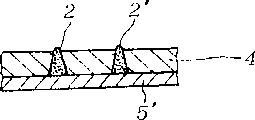
FIG. 5(a) is a sectional view of a main portion of a printed wiring board of the present invention; fig. 5(b) is a sectional view showing a mode of manufacturing embodiment of the printed wiring board shown in fig. 5 (a).
The printed circuit board according to this embodiment is a double-sided printed circuit board, as shown in fig. 5 (a). Here, 4' is a glass cloth-reinforced epoxy resin series thin plate layer (insulating layer); 3. 3 'is a copper pattern provided on both surfaces of the glass cloth-reinforced epoxy resin series thin plate layer 4'; and 2 is a through type conductor connection portion which is arranged to penetrate through the glass cloth reinforced epoxy resin thin sheet layer 4 'in the thickness direction and electrically connects the copper patterns 3, 3'.
In this configuration example, the tip portion of the substantially conical conductor projection of the through-type conductor wire 2 is formed and electrically connected to the surface of the copper pattern 3' by being pressed. It was also confirmed that the electric connection state formed by the substantially conical conductor projection has a connection resistance of 0.01 Ω or less, which is not problematic in a normal circuit.
Next, a method for manufacturing the printed wiring board having the above-described structure will be described by way of example. First, a conical recess having a height and a bottom diameter of 0.3mm was formed at a predetermined position of an aluminum plate having a thickness of 2 mm. Then, the molten eutectic solder is poured into the conical recess of the aluminum plate, and the solder is left only in the recess after scraping off the plate. On the surface of the residual solder, a copper pattern was arranged at a predetermined position in a molten state of the solder in the same manner as in example 1, and cooled in this manner to form a copper pattern having a substantially conical conductor bump group. Then, in the same manner as in example 1, 2 sheets of glass cloth-reinforced epoxy resin prepreg (synthetic resin sheet) 4 'having a thickness of 100 μm were prepared, and the copper patterns provided with the substantially conical conductor bumps were positioned relative to each other on the laminate on which the 2 sheets of synthetic resin sheet 4' were stacked.
Then, as in the case of example 1, a silicone rubber sheet having a thickness of 2mm was formed on the back surface of the synthetic resin sheet layer, and the sheet was laminated and disposed on a heat-sensitive adhesive sheet at 120 ℃Between the platens (not shown), 0.3MP is used although the aforementioned synthetic resin series sheet is plasticizedaThe resin was pressurized as a resin pressure, and the resin was taken out after cooling while maintaining the pressure. By such a process, the copper foil patterns of the substantially conical conductor projections and the support projections are pressed into the synthetic resin sheet while maintaining the above configuration, so that the female connector having a shape in which the respective tip portions of the substantially conical conductor are exposed from the synthetic resin sheet surface (corresponding to the structure shown in fig. 1) can be obtained.
As shown in the cross-section of FIG. 5(b), the female connector 1 thus formed was provided with a pattern 3 'of a 35 μm thick copper thin film formed on a support film by etching in advance, at a predetermined position on the exposed surface of the through-type conductor wiring portion 2 of the female connector 1, and was further arranged between hot press plates (not shown) at a temperature of 170 ℃ and a synthetic resin sheet 4'When reaching the thermoplastic state, the pressure 1MP is appliedaThe resin was held under pressure for 1 hour, cooled, and then taken out, and the supporting films supporting the copper foil patterns 3 and 3' were peeled off, whereby a printed wiring board shown by a cut surface in FIG. 5(a) was obtained.
It is considered that the double-sided printed circuit board manufactured as such does not have the problems of poor connection and poor reliability in conventional electrical inspection.
Further, the area of the conductor connecting portion 2 ' of the double-sided printed wiring board was cut in the thickness direction of the printed wiring board for detailed observation and study, and it was found that the conductor connecting portion 2 ' was inserted between the glass cloth meshes of the synthetic resin thin plate 4 '. That is, it is confirmed that breakage of glass fibers of the glass cloth as a reinforcing member is not observed, and migration due to breakage of the glass fibers does not occur, and the glass cloth has excellent electrical characteristics.
Example 3
Fig. 6(a) and (b) schematically show the implementation state of the present embodiment. First, a polyimide resin film (product name: カプトン film, manufactured by Toyolkk) having a thickness of 50 μm was prepared as a supporting base sheet 5, and a polymer-type silver-based electroconductive paste (product name: thermosetting electroconductive paste DW-250H-5; manufactured by Toyo Kagaku KK) and a metal mask having a hole having a diameter of 0.4mm were formed in a predetermined portion of a stainless steel sheet having a thickness of 200 μm were prepared.
Then, the metal mask is placed on the surface of the polyimide resin film 5 as specified, a conductive paste is printed, and after the printed conductive paste is dried, the conductive paste is repeatedly printed three times on the same position using the same mask, thereby forming the conductive bump 2 having a chevron shape of slightly less than 200 μm. On the other hand, a polyetherimine (ポリ) having a thickness of 100 μm was preparedIテルイミト) resin film (product name: スミライト FS-1400) manufacturing plant: sumitomo ベ - クライト KK)) as a synthetic resin sheet 4, and as shown in a cross section of fig. 6(a), a support base sheet 5 is disposed at a predetermined position on the synthetic resin sheet 4 toward the conductor projection 2 to be laminated. Thereafter, the synthetic resin thin plate 4 is laminated on the back surface thereof in the same manner as the support thin plate 5The polyimide resin film of (2) is used as the cover sheet 6. Followed by applying 1MPaThe laminate is pressed by a resin pressure to take out the pressed product, and the upper and lower thin plates 5 and 6 are peeled off, so that the conductor bump 2 is pressed into the synthetic resin film 4 as it is as shown in the cross section of FIG. 6(b), and the front end portion is pressed to be flush with the rear surface thin plate 6, thereby obtaining a printed wiring board having a conductor wiring portion 2' penetrating the synthetic resin thin plate 4 in the thickness direction thereof.
With the through-type conductor wiring portion 2' constructed as described above, the conduction conditions on the front and back sides were tested with a multimeter, and all data were less than 0.01 Ω.
Example 4
Fig. 7(a) and (b) are sectional views schematically showing an embodiment of the present embodiment. In this example, in the case of example 3, the electrolytic copper foil 5' having a thickness of 35 μm used in the production of a printed wiring board is generally used as the supporting base sheet 5 instead of the polyimide resin film. On the other hand, the same procedure as in example 3 of FIG. 6 was carried out except that an electrolytic copper foil 6' having the same thickness of 35 μm was used as the back sheet (cover sheet) 6. That is, as shown in FIG. 7(a), an electrolytic copper foil 5 'having a conductor bump 2 on one main surface, a synthetic resin-based thin plate 4 and an electrolytic copper foil 6' are laminated and arranged, and the laminate is press-worked at a temperature of 270 ℃ under a force of 1MPa to produce a double-sided copper-clad plate having a conductor wire portion 2 ', the conductor wire portion 2' being connected between the two copper foils 5 ', 6' through a through-connection, as shown in FIG. 7 (b). A normal etching protective layer ink (product name: PSR-4000H; manufacturer: Sun インキ KK) was screen-printed on 2 sides of the double-sided copper-clad plate, the conductor pattern portion was covered, and then etched with copper chloride as an etching solution, and the protective layer mask was peeled off to obtain a double-sided printed wiring board.
The double-sided printed wiring board thus manufactured was inspected for conventional electrical tests, and was found to be completely free from problems such as poor connection and poor reliability.
In addition, in the above, an electrolytic copper foil 6' is produced, and a zinc-plated copper foil is treated with chromic acid to form a chromate layer on the surface thereof (
) The double-sided printed wiring board was manufactured under the same conditions as described above except that the epoxy silane (or amino silane) was further treated. In the case of this double-sided printed wiring board, the outer conductor pattern exhibits excellent solder resistance, strength, and the like, and the characteristics thereof are good. That is, the surface of the synthetic resin
thin plate 4 is bonded with a chromate layer and a silane layer having a thickness of 0.01 μm, and the chromate layer is broken on the surface facing the tip of the conductor connecting portion 2' to form an electrical connection with the exposed new surface while the strength is improved.
Example 5
In the present example 3, instead of using a polyimide resin film as the supporting base sheet 5, a 35 μm electrolytic copper foil 5 ' having a thickness of 35 μm, which is generally used in the production of a printed circuit board, was used as the back sheet (cover sheet) 6, and a prepreg 4 ' having a thickness of 200 μm, in which a cover ring resin was impregnated into a glass cloth, was used as the synthetic resin sheet 4, and as shown in FIG. 7(a), electrolytic copper foils 5 ' and the like were stacked and placed on each other, and the stacked body was subjected to pressure application under the following conditionsAs shown in FIG. 7(b), a double-sided copper clad laminate having a lead connecting portion 2 ' penetrating and connecting between two copper foils 5 ', 6 ' is produced. The pressure processing is to heat the laminate to 120 deg.C to subject the resin to 2MPaThe pressure of (3) was further heated to 170 ℃ in this state, and the temperature was maintained for 1 hour, and then the mixture was cooled and taken out.
On both sides of the double-sided copper clad plate, a normal etching resist ink (product name: PSR-4000H, manufacturing plant: Sun (インキ KK) was screen-printed, after covering the conductor pattern portion, copper chloride was subjected to etching treatment as an etching solution, and then a resist mask was peeled off to obtain a double-sided printed wiring board, for the double-sided printed wiring board thus manufactured, no problems such as poor connection or poor reliability were found in the conventional electrical test, and in order to evaluate the connection reliability between the aforementioned two-sided conductive patterns, a hot oil test was performed (immersion in oil at 260 ℃ for 10 seconds, immersion in oil at 20 ℃ for 20 seconds for 1 cycle), no problems were found even if 500 cycles were performed.
Example 6
Fig. 8(a) and (b) are sectional views schematically showing an embodiment of the present embodiment. In this example, a synthetic resin sheet 4' having a thickness of 120 μm was formed by impregnating a PPS resin sheet (product name: トレン f3000, manufactured by Toho レ KK) into a glass cloth. Then, on both main surfaces of the synthetic resin series sheet 4', a conductor paste composed of silver powder having an average diameter of 1 μm and polysulfone resin was screen-printed with 300-mesh stainless steel to form a desired conductor pattern 7. Then, conductor bumps 2 each having a square side of 0.4mm and a height of 80 μm were formed on desired positions of the conductor pattern 7 using a 180-mesh stainless steel wire net.
As shown in fig. 8(a), a polyimide resin film 6.6 laminated arrangement using a synthetic resin-series sheet 4 as a cover plate is formed by molding conductor bumps 2 for interlayer connection on both sides. Thereafter, the laminate was subjected to press working at 295 ℃ to peel off the polyimide resin film 6.6, thereby forming a double-sided printed wiring board having a conductor wiring portion 2' penetrating and connecting between the conductor patterns 7 on both sides as shown in FIG. 8 (b).
The double-sided printed wiring board thus manufactured was subjected to a conventional electrical test, and no problems such as poor contact or poor reliability were found at all.
In the above, the conductor bump 2 having a square side of 0.4mm and a height of 80 μm is formed on one main surface or both main surfaces of the synthetic resin thin plate 4' by using a 180-mesh stainless steel wire net. Thereafter, the laminate was laminated with the polyimide resin film 6.6 as a cover sheet, and the polyimide resin film 6.6 was removed by pressing the laminate at 295 ℃ to obtain a substrate having a conductive land portion 2' penetrating between both surfaces. Conductor patterns connected to the conductor land portions 2' having exposed end faces are formed on both principal surfaces of the substrate. That is, a conductor paste composed of silver powder having an average particle diameter of1 μm and polysulfone resin was printed on both main surfaces of the substrate using 300-mesh stainless steel wire gauze to form a desired conductor pattern, thereby obtaining a double-sided printed wiring board. The double-sided printed wiring board thus obtained was subjected to a conventional electrical test, and no problems such as poor contact or poor reliability were found at all.
Example 7
Fig. 9(a) and (b) are sectional views schematically showing an implementation state of the present embodiment. As shown in FIG. 9(a), a double-sided wiring board prepared in the same manner as in example 5 was sandwiched between prepreg 4' obtained by impregnating a glass cloth of the same type as that used in example 5 with an epoxy resin and having a thickness of 100 μm, to form a laminate arrangement. The conductive bumps 2 of the same kind as used in example 5 were sandwiched between copper foils 5' formed and placed, and then the conductive bumps were stacked. This laminate was subjected to press working under the same conditions as in example 5 to prepare a double-sided copper clad laminate having a 4-layer structure in which the inner layer conductive patterns 7 and the inner layer conductive patterns 7 were connected to the surface copper foil 5' through-holes.
The 4-layer structure was then screen printed on both sides with conventional etching resist ink (product name: PSR-4000H; manufacturer: Sun インキ KK). After covering the conductor pattern part, carrying out corrosion treatment by using copper chloride as an etching solution, and stripping the protective layer mask to obtain the printed circuit board with a 4-layer structure. With respect to the 4-layer printed wiring board thus manufactured, no problems such as poor connection or poor reliability were found by conducting a conventional electrical test. In order to evaluate the reliability of the connection between the two conductive patterns, no problem was found even when 500 cycles of hot oil test (cycle of immersion in oil at 260 ℃ for 10 seconds and further immersion in oil at 20 ℃ for 20 seconds was used as 1 cycle). The reliability of the connection between the conductive (wiring) patterns is excellent as compared with the conventional copper plating method.
Example 8
Fig. 10(a) and (b) are sectional views schematically showing the embodiment of the present embodiment. As the supporting base sheet, copper foils 7', 7 ″ formed with conductive bumps 2 having different ratios of times of height are prepared on at least one surface of a conductive pattern previously processed into a desired structure (shape). Furthermore, the same kind of semi-cured dip 4 having a thickness of 100 μm and the same kind of electrolytic copper foil 5 'having a thickness of 35 μm used in example 5 were prepared as electrolytic copper foil 6' having a thickness of 35 μm for the back sheet (cover sheet) 6. Then, as shown in fig. 10(a), they are stacked. This laminate was subjected to hot press working under the same conditions as in example 5 to prepare a double-sided copper-clad laminate in which the inner layer conductor patterns 7 ', 7 ″ and the inner layer conductor patterns 7 ', 7 ″ were connected to the surface copper foil 5 ' so as to penetrate, as shown in fig. 10 (b).
On both sides of the double-sided copper-clad plate, an ink (product name: PSR-4000H; manufacturer: Sun インキ KK) for a usual etching resist was screen-printed to cover the conductor pattern portion. And then, carrying out corrosion treatment by using copper chloride as an etching solution, and stripping the protective layer mask to obtain the double-sided printed circuit board. With respect to the 4-layer printed wiring board thus manufactured, no problems such as poor connection or poor reliability were found by conducting a conventional electrical test. In order to evaluate the reliability of the connection between the double-sided conductive patterns, no problem was found even when the test was carried out 500 times in a hot oil test (cycle of immersion in oil at 260 ℃ for 10 seconds and immersion in oil at 20 ℃ for 20 seconds was 1 cycle). The reliability of the connection between the conductive (wiring) patterns is excellent as compared with the conventional copper plating method.
Example 9
This embodiment is substantially the same as the manufacturing process of the printed circuit board in embodiment 4, except for the structure replacing the conductive bump group. Reference is therefore made to the embodiment shown schematically in fig. 7(a) and (b). This embodiment is generally applied to an electrolytic copper foil 5' having a thickness of 35 μm used in the manufacture of printed wiring boards, instead of a polyimide resin film, as the supporting base sheet 5. Then, a plating resist was printed on the roughened surface of the copper foil 5', and then, a wiring pattern having an exposed surface with a diameter of 0.3mm was left at a predetermined position, copper and nickel were sequentially plated, and a copper layer having a height of about 100 μm and a nickel layer having a height of 10 μm were stacked on the exposed surface region, thereby forming a conductor bump having a thickness of about 110 μm as a whole. On the one hand, the copper foil 5 'on which the conductor bump was formed by the above-mentioned plating method was used, and on the other hand, as shown in FIG. 7(a), a laminated arrangement was made as in example 3 except that 35 μm electrolytic copper foil 6' having the same thickness was used as the back surface sheet (cover sheet) 6. Then, this laminate was subjected to press working under the same conditions as in example 3 to obtain a double-sided copper-clad plate having a conductor wire connecting portion 2 ' penetrating and connecting both copper foils 5 ', 6 ', as shown in fig. 7 (b).
On both sides of the double-sided copper clad plate, a usual etching resist ink (product name: PSR-4000H; manufacturing plant: Sun インキ KK) was screen-printed to cover the conductor pattern portion. And then, taking copper chloride as an etching solution for corrosion treatment, and stripping the protective layer mask to obtain the double-sided printed circuit board. The double-sided printed wiring board thus produced was subjected to an electrical test, and no problems of poor connection or poor reliability were found.
In addition, the same result can be obtained even when the conductive bump of the present invention is formed by a dip soldering method using a solder resist mask. Further, even when the conductive bump made of the conductive composition in another embodiment is formed by the plating method, a printed wiring board with a connection between wiring layers can be obtained.
Example 10
Fig. 11, 12, 13, and 14 schematically show an implementation state of the present embodiment. Firstly, preparing an electrolytic copper foil 5' with the thickness of 35 μm used in the manufacture of a printed circuit board as a supporting base sheet; on the other hand, bismaleimide triazine (ポリ)Iテルサルホン) as a binder, silver series conductive paste (product name: i- メツク H9141 bei-land paint KK), and a metal mask with a 0.3mm diameter hole opened at a certain position of a stainless steel plate having a thickness of 200 μm. Then, the metal mask is placed at a predetermined position on the surface of the copper foil (supporting substrate sheet) 5', and then the conductive paste is printed, and after the conductive paste printed is dried, the conductive paste is repeatedly printed three times at the same position by the same method using the same mask, thereby finallyforming the mountain-shaped projection 2 having a thickness of not more than 200 μm.
On the other hand, a polyetherimid (ポリ I- ラルイミド) resin film (product name: スミライト FS-1400, Sumitomo ベ - クライト KK) having a thickness of 100 μm was prepared as the synthetic resin-series sheet 4. Then, as shown by the cross-sectional view of FIG. 11, a support base sheet 5' is disposed at a predetermined position with respect to the synthetic resin sheet 4 with respect to the conductive bump 2 formed, thereby forming a laminate. Then, a silicone rubber sheet having a thickness of about 3mm was disposed as a pressure receiving member 8 on the back surface of the synthetic resin sheet 4, and then a cover plate 6 was placed thereon, and the sheet was placed in a press device with a heating, pressing and cooling mechanism, and the temperature was raised without pressing. When the temperature is raised to 250 ℃, the 3MP is carried out for 1 timeaUntil cooled. By this pressing, as shown by the cross-sectional view of FIG. 1 '2, the tips of the conductive protrusions 2 on the surface of the supporting base sheet 5' are held in their original shapes, and the laminate of the resin-based sheet 4 can be accurately obtainedAnd (3) a body.
Next, as shown in the cross section of FIG. 13, electrolytic copper foils 6 'each having a thickness of 35 μm were stacked on the front end penetrating surfaces of the laminated conductor bumps 2, and then a protective film (cover) was formed on the surface of each of the copper foils 6' by using a polyimide resin film. Then, the laminate was placed between hot press plates (not shown) maintained at 270 ℃ and 500KP was addedaAfter the synthetic resin sheet reached 270 ℃, 2MP was applied to the resin for the 2 nd timeaThe pressure of (a). After cooling while maintaining the above 2 nd pressing, the protective film (sheet) 6 was removed, andthe cross section was observed, and as shown by the cross section in FIG. 14, a copper foil 6' was bonded to the synthetic resin sheet 4 to obtain a laminate of the whole form. Each conductor bump 2 penetrating the synthetic resin sheet 4 is plastically deformed (pressed) at its tip on the surface abutting against the copper foil 6 ', and is connected to the surface of the copper foil 6' on the same plane. A substrate for a double-sided copper-clad printed wiring board is provided with a conductor wiring portion 2 ', and the conductor wiring portion 2' penetrates a synthetic resin sheet 4 in the thickness direction.
On both sides of the substrate for the double-sided copper-clad printed wiring board, a conventional etching resist ink (product name: PSR-4000H, Sun インキ KK) was screen-printed to cover the conductor pattern. Then, copper chloride was used as an etching solution to perform etching treatment, and the resist mask was removed to obtain a double-sided printed wiring board. With respect to the double-sided printed wiring board thus obtained, no problems of poor contact or poor reliability were found by conducting a conventional electrical test.
In the present embodiment, the aluminum foil having a thickness of about 15 μm is interposed between the pressure receiving member 8 and the flat surface of the synthetic resin-based thin plate 4 by 1 pressing process, so that the conductive bumps 2 are inserted (penetrated) into the synthetic resin thin plate 4 more reliably while maintaining a good positional accuracy, and the bumps of the synthetic resin thin plate 4 in the peripheral portion of the conductive connection portion 2' to be formed can be reliably prevented.
In the above, as the electrolytic copper foil 6', in addition to the chromate treatment of the galvanized copper foil with chromic acid, a chromate layer (
) Treating with epoxy silane (or aminosilane), and making double-sided printed circuit by the same conditionsAnd (3) a plate. In the case of this double-sided printed wiring board, the outer conductor pattern exhibits excellent solder resistance, peel strength, and the like. In any case, the conductor pattern is bonded to the surface of the
synthetic resin sheet 4 by a chromate layer having a thickness of about 0.01 μm and a silane layer. The chromate layer is broken on the surface facing the tip of the conductor connecting portion 2' to form a structure for electrical connection with the exposed new surface.
Example 11
Fig. 15(a) and (b) are sectional views schematically showing the state of the present embodiment. In this example 10, a substrate for a single-sided copper-clad printed wiring board with a conductor terminal portion 2' having a tip end of a conductor projection 2 plastically deformed to be in close contact with a copper foil and the other end penetrating a synthetic resin sheet 4 in a thickness direction in an exposed shape was produced as shown in fig. 15(b) by laminating the laminate as in example 10 except that a polyimide resin film having a thickness of 50 μm was used as the supporting base sheet 5 as shown in fig. 15(a), and subjecting the laminate to press treatment once and then to press treatment 2 times under the same conditions.
On the copper foil 6' side of the printed wiring board substrate, a conventional etching resist ink (product name: PSR-4000H Sun インキ KK) was screen-printed to cover the conductor pattern portion. Then, copper chloride is used as an etching solution to carry out etching treatment, and then the resist mask is peeled off to obtain a double-sided printed wiring board having a conductor wiring portion 2' penetrating therethrough. Conventional electrical tests were conducted on the printed wiring boards thus produced, and no problems of poor connection or poor reliability were found.
The end face of the conductor terminal portion 2' penetrating the one principal surface can be used as a connection boss and a lead terminal on an exposed printed wiring board, and is suitable for a back-surface mounting type mounted circuit device, for example.
Example 12
This example was carried out in the same manner as example 10 except that in example 10, a synthetic resin-based sheet 4 was formed by impregnating a glass cloth with an epoxy resin to form a 200 μm thick semi-cured dip 4'. First, the laminate was put into a pressurizing apparatus, heated to 120 ℃ and 2MP was appliedaThe resin was pressurized, cooled and the primary pressurized product was taken out. Then, a copper foil 6' was placed and heated, and 2MP was applied to the resinaIs heated to 170 ℃ and held for 1 hour, and then cooled, and then subjected to pressing 2 times in a manner of taking out, to thereby produce a substrate for a double-sided copper-clad printed wiring board having a conductor wiring portion 2 ' penetrating and connecting between two copper foils 5 ', 6 '.
The double-sided copper-clad printed wiring board substrate was screen-printed on both sides with a normal etching resist ink (product name: PSR 4000H, sun インキ KK), covered with the conductor pattern portion, etched with copper chloride as an etching solution, and then peeled off from the resist mask to obtain a double-sided printed wiring board. The double-sided printed circuit board thus manufactured was subjected to a conventional electrical test without any problems of poor connection or poor reliability. In order to evaluate the reliability of the connection between the double-sided conductive patterns, no connection failure was observed even when the test was performed 500 times in a hot oil test (cycle of immersion in oil at260 ℃ for 10 seconds and immersion in oil at 20 ℃ for 20 seconds was 1 cycle). The connection reliability between the conductive (wiring) pattern layers is excellent as compared with the conventional copper plating method.
Further, the conductor connecting portion 2 'of the double-sided printed circuit is cut in the thickness direction of the printed circuit board, and the conductor connecting portion 2' is found to penetrate between the meshes of the glass cloth of the synthetic rubber-based thin plate 4 by a detailed observation and study. That is, no problem such as breakage of the glass fibers of the glass cloth constituting the reinforcement body was observed. It has therefore been determined that migration due to the aforementioned breakage of the glass fibers does not occur (マイグレ - ミヨン), and that the weather-resistant properties are good.
Example 13
Fig. 16(a) and (b) are sectional views schematically showing other embodiments of the present embodiment. In this example, a PPS resin (product name: トレリ f3000, east レ KK) was impregnated into a glass fiber cloth having a cross pitch of 0.4mm to form a belt-shaped synthetic resin-series sheet 4' having a thickness of 125 μm and a width of 300 mm; a tape 5 ' was also prepared by molding a conductor bump 2 having a square bottom side of 0.3mm and a mountain height of 250 μm using a conductor paste composed of silver powder having an average particle diameter of 1 μm and polysulfone resin with a metal mesh having through holes of 0.3mm in diameter formed at predetermined positions on one main surface of a tape-shaped support sheet 5 ' composed of an electrodeposited copper foil of 35 μm in thickness and 350mm in width, to thereby form a tape 5 '. A tape-shaped electrolytic copper foil 6' having a thickness of 18 μm and a width of 350mm and an aluminum tape 9 having a thickness of 150 μm and a width of 400mm were also prepared. On the other hand, a 1 st double roller device having a rubber roller 10 (an internally heated member functioning as a pressure receiving body 8) and a metal roller 11 (functioning as a crop pressure receiving body) and a 2 nd double roller device having a pair of internally heated metal rollers 11' (functioning as a pressure receiving body) are provided.
Then, the tape-shaped support base sheet 5 ″ provided with the conductor bumps 2, the tape-shaped synthetic resin-based sheet 4 ', and the aluminum tape 9 are passed between the rubber roller 10 and the metal roller 11 (heated to 190 ℃) of the 1 st double-roller device and pressed while being wound around rollers (not shown) on which the tape-shaped support base sheet 5 ″, the tape-shaped synthetic resin-based sheet 4', and the aluminum tape 9 are formed. Even if the supporting base sheet 5 ″ is made of a synthetic resin thin sheet 4 ' and an aluminum tape 9, the synthetic resin thin sheet 4 ' and the aluminum tape are sequentially laminated and passed through the metal roller 11, and the synthetic resin thin sheet 4 ' is inserted (passed) through the projections 2 on the surface of the supporting base sheet 5 ″ by pressing (1 time pressing). Here, the aluminum tape 9 is separated from the prepared laminate, and if the laminate is wound on a roll, the following steps can be easily performed.
The laminate was then placed on a 2 nd double roller apparatus and pressed 2 times. That is, the tape-shaped electrolytic copper foil 6 ″ is laminated on the surface of the laminate projection 2 through which the tip is exposed, and passed between the hot metal rolls 11' set at 300 ℃ of the 2 nd double roll apparatus. While passing between the metal rolls 11 ', the synthetic resin-based sheet 4' is locally softened and integrated with the electrolytic copper foil 6 ″. On the other hand, the tips of the projections 2 inserted and exposed are tightly connected to the electrolytic copper foil 6' by plastic deformation. Thus, a double-sided printed wiring board substrate having a conductor wiring portion 2 ' penetrating and connecting between the two electrolytic copper foils 5 ' and 6 ' is manufactured.
The double-sided printed wiring board substrate was patterned in the same manner as in example 10 to produce a double-sided printed wiring board, and was electrically inspected conventionally, and no problems such as poor connection and poor reliability were observed.
Example 14
Fig. 17(a) and (b) are sectional views schematically showing other embodiments of the present embodiment.
First, a desired conductive paste wiring pattern 7' was formed by screen printing on both surfaces of an epoxy resin thin plate 5 made of 100 μm thick glass cloth. Then, a double-sided wiring type supporting base sheet 5 having conductor bumps 2 of 0.3mm in diameter and 0.3mm in height formed on a surface of a predetermined position of the conductive paste series wiring pattern 7' formed as described above was prepared. As shown in fig. 17(a), the double-sided wiring type support base sheet 5 was laminated and arranged by sandwiching the sheet 4 'by 2 sheets of epoxy resin-based prepreg sheets 4' each having a glass cloth of 100 μm in thickness as a base material. Further, silicone rubber sheets 8 as pressure receiving members were disposed on both surfaces of the sheet through thin aluminum foil 9, and subjected to pressure treatment 1 time in a hot state. This pressure treatment allows the conductive bumps 2 on the surface of the support base sheet 5 'to penetrate through the prepreg sheet 4' of various epoxy resin series in the thickness direction and to be exposed.
Next, an electrolytic copper foil 6' and a resin film as a protective film were sequentially laminated onboth surfaces of the laminate conductive bump 2 exposed at the tip end, and hot press processing (2-time press) hardening treatment was performed. By the 2-time press hardening treatment, the molding surface of the inner layer conductor pattern 7 ', the surface of the support base sheet 5, and the surface of the electrolytic copper foil 6' are integrally fused with each other. Fig. 17(b) shows a cross section of the double-sided copper-clad printed wiring board thus produced, and the inner layer conductor (wiring) pattern 7 'is a 4-layer double-sided copper-clad printed wiring board having a reliable connection structure of a through type on the surface copper foil 6'.
Then, a normal etching resist ink was screen-printed on both sides of the double-sided copper clad plate having the 4-layer structure to cover the conductor pattern portion, and then, etching treatment was performed using copper chloride as an etching solution. Then, the protective layer mask is peeled off to obtain a double-sided printed circuit board. The printed wiring board thus obtained was subjected to conventional electrical inspection, and no problems such as poor connection were found. In order to evaluate the reliability of the connection between the inner and outer layer wiring patterns, no problem was found even when the test was performed 500 times by using a hot oil test (cycle of immersion in oil at 260 ℃ for 10 seconds and immersion in oil at 20 ℃ for 20 seconds as one cycle). Compared with the conventional copper plating method, the reliability of connection between wiring patterns is excellent.
Example 15
In the above embodiment 11, the printed circuit board is manufactured by substantially the same process except for the structure in place of the conductor bump group. Therefore, the description will be made with reference to the embodiment schematically shown in fig. 13 and 14. In this example, an electrolytic copper foil5' having a thickness of 35 μm was used as the supporting base sheet 5 in place of the polyimide resin film, and a plating resist was printed on the roughened surface of the copper foil 5. Thereafter, patterning was performed at a predetermined position (place) with an exposed surface having a diameter of 0.3mm, and copper plating and gold plating were sequentially performed, so that a copper layer having a height of about 100 μm and a gold layer having a height of about 10 μm were stacked on the exposed surface region, thereby forming a conductor bump 2 having a height of about 110 μm as a whole.
On the other hand, a 100 μm thick polyetherimine resin film (product name: スミライ) was preparedト FS-1400 sumitomo ベ - クライト KK) as the synthetic resin series sheet 4. Then, the conductive bumps formed on the synthetic resin-based sheet 4) were placed at predetermined positions in opposition to a supporting base sheet 5' and an aluminum foil 15 μm thick to form a laminate. Thereafter, a silicone rubber sheet having a thickness of 3mm was disposed as a pressure receiving member 8 on the back surface of the synthetic resin sheet 4. Heating to 260 deg.C from the back of the supporting substrate sheet 5', and applying 3MP 1 timeaAs the pressure against the resin. This 1-time pressing provides a laminate in which the tips of the conductive bumps 2 on the surface of the support base sheet 5' are maintained in their original shapes and the synthetic resin sheet 4 is accurately inserted.
Next, as shown in FIG. 13, an electrolytic copper foil 6' having a thickness of 18 μm was laminated on the penetrating surface of the tip of the conductor bump 2, and a polyimide resin film was disposed as a protective film on the surface of the copper foil 6. Then disposed between hot press plates (not shown) maintained at 270 deg.C, and heated at 2MP when the synthetic resin sheet 4 is in a thermoplastic stateaThe pressure was applied to the resin 2 times. The sheet was cooled under the secondary pressure and then taken out, and the protective film 8 was peeled off and the cross section thereof was observed, whereby a double-sided copper-clad printed wiring board substrate in which copper foils 5 'and 6' were integrally bonded to the synthetic resin sheet 4 was obtained as shown in the cross section of FIG. 14. The printed wiring board is then provided with conductor wiring portions 2' of which each conductive bump 2 penetrating through the synthetic resin sheet 4 is on the surface abutting against the copper foil 6The tip end of the copper foil is plastically deformed (deformed) to form a flat surface, is connected to the surface of the copper foil 6', and penetrates the synthetic resin sheet 4 in the thickness direction.
On both sides of the double-sided copper-clad plate, a normal etching resist ink (product name: PSR-4000H Sun インキ KK) was screen-printed, and after covering the conductor pattern portion, etching treatment was performed using copper chloride as an etching solution. The protective layer mask is then stripped to obtain a double-sided printed circuit board. With respect to the double-sided printed wiring board thus obtained, the resistance of each through-type conductor terminal portion 8 was 0.01 Ω or less by a conventional electrical test, and no problems such as poor contact or poor reliability were found.
The conductor bump of the present invention is formed by a solder dip method in which the solder pot (half-field bath) is immersed in a tin pot set at a low temperature through a solder resist mask, and the same result can be obtained even when the mountain-shaped conductor bump 2 is formed. Further, even when the bump group composed of the conductive composition in the other examples was formed by the plating method, a printed wiring board having connection between the terminal layers could beobtained.
As is apparent from the above description, in the circuit component of the present invention, the conductor wire connecting portion penetrating the insulating support substrate in the thickness direction is formed by inserting, for example, a conductor projection formed in a conical shape under pressure. The manufacturing process is easy, and even a very small through-type conductor connection portion can be set with high precision at a definite set position, which is also helpful for greatly improving the reliability of the electrical connection between the two surfaces. In a word, in the process of forming the through conductor wiring portion, a hole forming process, an electroplating process and the like are not required, so that problems occurring in the manufacturing process are greatly reduced, and the yield is improved. On the other hand, an internal connection and a multilayer wiring board with high reliability are obtained. By using the internal connection and multilayer wiring board, the component mounting density and the wiring density can be greatly improved, the mounting region can be set regardless of the position of the connection hole, and the distance between the mounted electronic components can be shortened, so that the circuit performance can be improved. In summary, it can be said that the present invention contributes not only to reduction in the cost of the inner connection and the wiring board, but also to miniaturization and high performance of the mounted circuit device.