CN105358473B - Wafer level package solder barrier for use as a vacuum getter - Google Patents
Wafer level package solder barrier for use as a vacuum getter Download PDFInfo
- Publication number
- CN105358473B CN105358473B CN201480039124.9A CN201480039124A CN105358473B CN 105358473 B CN105358473 B CN 105358473B CN 201480039124 A CN201480039124 A CN 201480039124A CN 105358473 B CN105358473 B CN 105358473B
- Authority
- CN
- China
- Prior art keywords
- barrier
- layer
- substrate
- solder
- getter
- Prior art date
- Legal status (The legal status is an assumption and is not a legal conclusion. Google has not performed a legal analysis and makes no representation as to the accuracy of the status listed.)
- Active
Links
- 230000004888 barrier function Effects 0.000 title claims abstract description 189
- 229910000679 solder Inorganic materials 0.000 title claims abstract description 83
- 239000000463 material Substances 0.000 claims abstract description 239
- 239000010936 titanium Substances 0.000 claims abstract description 79
- RTAQQCXQSZGOHL-UHFFFAOYSA-N Titanium Chemical compound [Ti] RTAQQCXQSZGOHL-UHFFFAOYSA-N 0.000 claims abstract description 77
- 229910052719 titanium Inorganic materials 0.000 claims abstract description 77
- 238000000034 method Methods 0.000 claims abstract description 31
- 238000004519 manufacturing process Methods 0.000 claims abstract description 13
- 239000000758 substrate Substances 0.000 claims description 135
- 238000007789 sealing Methods 0.000 claims description 82
- 230000000903 blocking effect Effects 0.000 claims description 20
- 238000000151 deposition Methods 0.000 claims description 19
- 230000003213 activating effect Effects 0.000 claims description 7
- MAKDTFFYCIMFQP-UHFFFAOYSA-N titanium tungsten Chemical compound [Ti].[W] MAKDTFFYCIMFQP-UHFFFAOYSA-N 0.000 claims description 7
- 238000010438 heat treatment Methods 0.000 claims description 2
- 235000012431 wafers Nutrition 0.000 description 61
- 239000007767 bonding agent Substances 0.000 description 26
- 229910052751 metal Inorganic materials 0.000 description 25
- 239000002184 metal Substances 0.000 description 25
- 230000005855 radiation Effects 0.000 description 22
- XUIMIQQOPSSXEZ-UHFFFAOYSA-N Silicon Chemical compound [Si] XUIMIQQOPSSXEZ-UHFFFAOYSA-N 0.000 description 21
- 229910052710 silicon Inorganic materials 0.000 description 21
- 239000010703 silicon Substances 0.000 description 21
- 238000005247 gettering Methods 0.000 description 16
- 239000010931 gold Substances 0.000 description 15
- PCHJSUWPFVWCPO-UHFFFAOYSA-N gold Chemical compound [Au] PCHJSUWPFVWCPO-UHFFFAOYSA-N 0.000 description 14
- 229910052737 gold Inorganic materials 0.000 description 14
- 238000010586 diagram Methods 0.000 description 12
- PXHVJJICTQNCMI-UHFFFAOYSA-N Nickel Chemical compound [Ni] PXHVJJICTQNCMI-UHFFFAOYSA-N 0.000 description 11
- 230000004913 activation Effects 0.000 description 11
- 230000003287 optical effect Effects 0.000 description 8
- 230000008569 process Effects 0.000 description 8
- 238000006243 chemical reaction Methods 0.000 description 7
- 238000003491 array Methods 0.000 description 6
- 239000000203 mixture Substances 0.000 description 5
- 229910052759 nickel Inorganic materials 0.000 description 5
- BASFCYQUMIYNBI-UHFFFAOYSA-N platinum Chemical compound [Pt] BASFCYQUMIYNBI-UHFFFAOYSA-N 0.000 description 5
- 230000008021 deposition Effects 0.000 description 4
- 238000005538 encapsulation Methods 0.000 description 4
- 150000002739 metals Chemical class 0.000 description 4
- -1 organic vapors Substances 0.000 description 4
- 229920000642 polymer Polymers 0.000 description 4
- 239000004065 semiconductor Substances 0.000 description 4
- 238000009736 wetting Methods 0.000 description 4
- 239000004568 cement Substances 0.000 description 3
- 239000000919 ceramic Substances 0.000 description 3
- 238000005286 illumination Methods 0.000 description 3
- 239000007788 liquid Substances 0.000 description 3
- 239000000126 substance Substances 0.000 description 3
- 230000004075 alteration Effects 0.000 description 2
- 230000008859 change Effects 0.000 description 2
- 238000005530 etching Methods 0.000 description 2
- 238000001125 extrusion Methods 0.000 description 2
- 239000007789 gas Substances 0.000 description 2
- JVPLOXQKFGYFMN-UHFFFAOYSA-N gold tin Chemical compound [Sn].[Au] JVPLOXQKFGYFMN-UHFFFAOYSA-N 0.000 description 2
- 238000005469 granulation Methods 0.000 description 2
- 230000003179 granulation Effects 0.000 description 2
- 238000005259 measurement Methods 0.000 description 2
- 229920002120 photoresistant polymer Polymers 0.000 description 2
- 229910052697 platinum Inorganic materials 0.000 description 2
- 238000012545 processing Methods 0.000 description 2
- 238000006467 substitution reaction Methods 0.000 description 2
- 229910008599 TiW Inorganic materials 0.000 description 1
- ATJFFYVFTNAWJD-UHFFFAOYSA-N Tin Chemical compound [Sn] ATJFFYVFTNAWJD-UHFFFAOYSA-N 0.000 description 1
- NRTOMJZYCJJWKI-UHFFFAOYSA-N Titanium nitride Chemical compound [Ti]#N NRTOMJZYCJJWKI-UHFFFAOYSA-N 0.000 description 1
- 239000002253 acid Substances 0.000 description 1
- 150000007513 acids Chemical class 0.000 description 1
- 230000006978 adaptation Effects 0.000 description 1
- QVGXLLKOCUKJST-UHFFFAOYSA-N atomic oxygen Chemical compound [O] QVGXLLKOCUKJST-UHFFFAOYSA-N 0.000 description 1
- 230000008901 benefit Effects 0.000 description 1
- 239000007795 chemical reaction product Substances 0.000 description 1
- 239000011248 coating agent Substances 0.000 description 1
- 238000000576 coating method Methods 0.000 description 1
- 238000011109 contamination Methods 0.000 description 1
- 238000000708 deep reactive-ion etching Methods 0.000 description 1
- 238000005137 deposition process Methods 0.000 description 1
- 238000003795 desorption Methods 0.000 description 1
- 238000001514 detection method Methods 0.000 description 1
- 239000003989 dielectric material Substances 0.000 description 1
- 230000007613 environmental effect Effects 0.000 description 1
- 239000011521 glass Substances 0.000 description 1
- 239000001257 hydrogen Substances 0.000 description 1
- 229910052739 hydrogen Inorganic materials 0.000 description 1
- 125000004435 hydrogen atom Chemical class [H]* 0.000 description 1
- 239000012535 impurity Substances 0.000 description 1
- 238000007689 inspection Methods 0.000 description 1
- 239000012212 insulator Substances 0.000 description 1
- 230000008018 melting Effects 0.000 description 1
- 238000002844 melting Methods 0.000 description 1
- 125000002496 methyl group Chemical group [H]C([H])([H])* 0.000 description 1
- 238000012986 modification Methods 0.000 description 1
- 230000004048 modification Effects 0.000 description 1
- 150000001282 organosilanes Chemical class 0.000 description 1
- 239000001301 oxygen Substances 0.000 description 1
- 229910052760 oxygen Inorganic materials 0.000 description 1
- 238000004806 packaging method and process Methods 0.000 description 1
- 230000000149 penetrating effect Effects 0.000 description 1
- 229920000307 polymer substrate Polymers 0.000 description 1
- 229920001296 polysiloxane Polymers 0.000 description 1
- 238000002360 preparation method Methods 0.000 description 1
- 229910052594 sapphire Inorganic materials 0.000 description 1
- 239000010980 sapphire Substances 0.000 description 1
- 238000000926 separation method Methods 0.000 description 1
- HBMJWWWQQXIZIP-UHFFFAOYSA-N silicon carbide Chemical compound [Si+]#[C-] HBMJWWWQQXIZIP-UHFFFAOYSA-N 0.000 description 1
- 230000007480 spreading Effects 0.000 description 1
- 238000003892 spreading Methods 0.000 description 1
- 238000004544 sputter deposition Methods 0.000 description 1
- MZLGASXMSKOWSE-UHFFFAOYSA-N tantalum nitride Chemical compound [Ta]#N MZLGASXMSKOWSE-UHFFFAOYSA-N 0.000 description 1
- 238000012546 transfer Methods 0.000 description 1
- 238000007738 vacuum evaporation Methods 0.000 description 1
- 238000007740 vapor deposition Methods 0.000 description 1
- XLYOFNOQVPJJNP-UHFFFAOYSA-N water Substances O XLYOFNOQVPJJNP-UHFFFAOYSA-N 0.000 description 1
- 229910001868 water Inorganic materials 0.000 description 1
Images


Classifications
-
- H—ELECTRICITY
- H01—ELECTRIC ELEMENTS
- H01L—SEMICONDUCTOR DEVICES NOT COVERED BY CLASS H10
- H01L23/00—Details of semiconductor or other solid state devices
- H01L23/02—Containers; Seals
- H01L23/10—Containers; Seals characterised by the material or arrangement of seals between parts, e.g. between cap and base of the container or between leads and walls of the container
-
- B—PERFORMING OPERATIONS; TRANSPORTING
- B81—MICROSTRUCTURAL TECHNOLOGY
- B81B—MICROSTRUCTURAL DEVICES OR SYSTEMS, e.g. MICROMECHANICAL DEVICES
- B81B7/00—Microstructural systems; Auxiliary parts of microstructural devices or systems
- B81B7/0032—Packages or encapsulation
- B81B7/0035—Packages or encapsulation for maintaining a controlled atmosphere inside of the chamber containing the MEMS
- B81B7/0038—Packages or encapsulation for maintaining a controlled atmosphere inside of the chamber containing the MEMS using materials for controlling the level of pressure, contaminants or moisture inside of the package, e.g. getters
-
- B—PERFORMING OPERATIONS; TRANSPORTING
- B81—MICROSTRUCTURAL TECHNOLOGY
- B81C—PROCESSES OR APPARATUS SPECIALLY ADAPTED FOR THE MANUFACTURE OR TREATMENT OF MICROSTRUCTURAL DEVICES OR SYSTEMS
- B81C1/00—Manufacture or treatment of devices or systems in or on a substrate
- B81C1/00015—Manufacture or treatment of devices or systems in or on a substrate for manufacturing microsystems
- B81C1/00261—Processes for packaging MEMS devices
- B81C1/00269—Bonding of solid lids or wafers to the substrate
-
- H—ELECTRICITY
- H01—ELECTRIC ELEMENTS
- H01L—SEMICONDUCTOR DEVICES NOT COVERED BY CLASS H10
- H01L21/00—Processes or apparatus adapted for the manufacture or treatment of semiconductor or solid state devices or of parts thereof
- H01L21/02—Manufacture or treatment of semiconductor devices or of parts thereof
- H01L21/04—Manufacture or treatment of semiconductor devices or of parts thereof the devices having at least one potential-jump barrier or surface barrier, e.g. PN junction, depletion layer or carrier concentration layer
- H01L21/50—Assembly of semiconductor devices using processes or apparatus not provided for in a single one of the subgroups H01L21/06 - H01L21/326, e.g. sealing of a cap to a base of a container
- H01L21/52—Mounting semiconductor bodies in containers
-
- H—ELECTRICITY
- H01—ELECTRIC ELEMENTS
- H01L—SEMICONDUCTOR DEVICES NOT COVERED BY CLASS H10
- H01L21/00—Processes or apparatus adapted for the manufacture or treatment of semiconductor or solid state devices or of parts thereof
- H01L21/70—Manufacture or treatment of devices consisting of a plurality of solid state components formed in or on a common substrate or of parts thereof; Manufacture of integrated circuit devices or of parts thereof
- H01L21/71—Manufacture of specific parts of devices defined in group H01L21/70
- H01L21/768—Applying interconnections to be used for carrying current between separate components within a device comprising conductors and dielectrics
- H01L21/76838—Applying interconnections to be used for carrying current between separate components within a device comprising conductors and dielectrics characterised by the formation and the after-treatment of the conductors
- H01L21/76841—Barrier, adhesion or liner layers
-
- H—ELECTRICITY
- H01—ELECTRIC ELEMENTS
- H01L—SEMICONDUCTOR DEVICES NOT COVERED BY CLASS H10
- H01L23/00—Details of semiconductor or other solid state devices
- H01L23/16—Fillings or auxiliary members in containers or encapsulations, e.g. centering rings
- H01L23/18—Fillings characterised by the material, its physical or chemical properties, or its arrangement within the complete device
- H01L23/26—Fillings characterised by the material, its physical or chemical properties, or its arrangement within the complete device including materials for absorbing or reacting with moisture or other undesired substances, e.g. getters
-
- H—ELECTRICITY
- H01—ELECTRIC ELEMENTS
- H01L—SEMICONDUCTOR DEVICES NOT COVERED BY CLASS H10
- H01L23/00—Details of semiconductor or other solid state devices
- H01L23/48—Arrangements for conducting electric current to or from the solid state body in operation, e.g. leads, terminal arrangements ; Selection of materials therefor
- H01L23/488—Arrangements for conducting electric current to or from the solid state body in operation, e.g. leads, terminal arrangements ; Selection of materials therefor consisting of soldered or bonded constructions
- H01L23/498—Leads, i.e. metallisations or lead-frames on insulating substrates, e.g. chip carriers
- H01L23/49866—Leads, i.e. metallisations or lead-frames on insulating substrates, e.g. chip carriers characterised by the materials
-
- H—ELECTRICITY
- H01—ELECTRIC ELEMENTS
- H01L—SEMICONDUCTOR DEVICES NOT COVERED BY CLASS H10
- H01L27/00—Devices consisting of a plurality of semiconductor or other solid-state components formed in or on a common substrate
- H01L27/14—Devices consisting of a plurality of semiconductor or other solid-state components formed in or on a common substrate including semiconductor components sensitive to infrared radiation, light, electromagnetic radiation of shorter wavelength or corpuscular radiation and specially adapted either for the conversion of the energy of such radiation into electrical energy or for the control of electrical energy by such radiation
- H01L27/144—Devices controlled by radiation
- H01L27/146—Imager structures
- H01L27/14601—Structural or functional details thereof
- H01L27/14618—Containers
-
- H—ELECTRICITY
- H01—ELECTRIC ELEMENTS
- H01L—SEMICONDUCTOR DEVICES NOT COVERED BY CLASS H10
- H01L27/00—Devices consisting of a plurality of semiconductor or other solid-state components formed in or on a common substrate
- H01L27/14—Devices consisting of a plurality of semiconductor or other solid-state components formed in or on a common substrate including semiconductor components sensitive to infrared radiation, light, electromagnetic radiation of shorter wavelength or corpuscular radiation and specially adapted either for the conversion of the energy of such radiation into electrical energy or for the control of electrical energy by such radiation
- H01L27/144—Devices controlled by radiation
- H01L27/146—Imager structures
- H01L27/14601—Structural or functional details thereof
- H01L27/14634—Assemblies, i.e. Hybrid structures
-
- H—ELECTRICITY
- H01—ELECTRIC ELEMENTS
- H01L—SEMICONDUCTOR DEVICES NOT COVERED BY CLASS H10
- H01L27/00—Devices consisting of a plurality of semiconductor or other solid-state components formed in or on a common substrate
- H01L27/14—Devices consisting of a plurality of semiconductor or other solid-state components formed in or on a common substrate including semiconductor components sensitive to infrared radiation, light, electromagnetic radiation of shorter wavelength or corpuscular radiation and specially adapted either for the conversion of the energy of such radiation into electrical energy or for the control of electrical energy by such radiation
- H01L27/144—Devices controlled by radiation
- H01L27/146—Imager structures
- H01L27/14601—Structural or functional details thereof
- H01L27/14636—Interconnect structures
-
- H—ELECTRICITY
- H01—ELECTRIC ELEMENTS
- H01L—SEMICONDUCTOR DEVICES NOT COVERED BY CLASS H10
- H01L27/00—Devices consisting of a plurality of semiconductor or other solid-state components formed in or on a common substrate
- H01L27/14—Devices consisting of a plurality of semiconductor or other solid-state components formed in or on a common substrate including semiconductor components sensitive to infrared radiation, light, electromagnetic radiation of shorter wavelength or corpuscular radiation and specially adapted either for the conversion of the energy of such radiation into electrical energy or for the control of electrical energy by such radiation
- H01L27/144—Devices controlled by radiation
- H01L27/146—Imager structures
- H01L27/14683—Processes or apparatus peculiar to the manufacture or treatment of these devices or parts thereof
- H01L27/1469—Assemblies, i.e. hybrid integration
-
- B—PERFORMING OPERATIONS; TRANSPORTING
- B81—MICROSTRUCTURAL TECHNOLOGY
- B81B—MICROSTRUCTURAL DEVICES OR SYSTEMS, e.g. MICROMECHANICAL DEVICES
- B81B2201/00—Specific applications of microelectromechanical systems
- B81B2201/02—Sensors
- B81B2201/0207—Bolometers
-
- B—PERFORMING OPERATIONS; TRANSPORTING
- B81—MICROSTRUCTURAL TECHNOLOGY
- B81C—PROCESSES OR APPARATUS SPECIALLY ADAPTED FOR THE MANUFACTURE OR TREATMENT OF MICROSTRUCTURAL DEVICES OR SYSTEMS
- B81C2203/00—Forming microstructural systems
- B81C2203/03—Bonding two components
- B81C2203/033—Thermal bonding
- B81C2203/035—Soldering
-
- H—ELECTRICITY
- H01—ELECTRIC ELEMENTS
- H01L—SEMICONDUCTOR DEVICES NOT COVERED BY CLASS H10
- H01L2224/00—Indexing scheme for arrangements for connecting or disconnecting semiconductor or solid-state bodies and methods related thereto as covered by H01L24/00
- H01L2224/01—Means for bonding being attached to, or being formed on, the surface to be connected, e.g. chip-to-package, die-attach, "first-level" interconnects; Manufacturing methods related thereto
- H01L2224/10—Bump connectors; Manufacturing methods related thereto
- H01L2224/15—Structure, shape, material or disposition of the bump connectors after the connecting process
- H01L2224/16—Structure, shape, material or disposition of the bump connectors after the connecting process of an individual bump connector
-
- H—ELECTRICITY
- H01—ELECTRIC ELEMENTS
- H01L—SEMICONDUCTOR DEVICES NOT COVERED BY CLASS H10
- H01L2924/00—Indexing scheme for arrangements or methods for connecting or disconnecting semiconductor or solid-state bodies as covered by H01L24/00
- H01L2924/0001—Technical content checked by a classifier
- H01L2924/0002—Not covered by any one of groups H01L24/00, H01L24/00 and H01L2224/00
Abstract
An electronic device and a method of manufacturing the same. One or more methods may include providing a cap wafer having a cavity and a surface surrounding the cavity and a device wafer having a detector device and a reference device. In some examples, a solder barrier layer of titanium material may be deposited onto the surface of the cap wafer. The solder barrier layer of titanium material may also be activated to act as a getter. In various examples, the cap wafer and the device wafer may be bonded together using solder, and the solder barrier layer of titanium material may prevent the solder from contacting the surface of the cap wafer.
Description
Technical Field
Background
A packaged Focal Plane Array (FPA) may include a detector array, an associated reference detector array, readout circuitry, and a transmissive cover that encapsulates one or more of these structures. The transmissive cover may be sealed via a sealing structure such as a sealing ring. The sealed structure may include two components, a first component located on the transmissive cover and a second component located on a substrate containing the detector array, the reference array and the readout circuitry. The two components may be aligned and welded together to seal the two components together.
In some cases, one of the surfaces of the transmissive enclosure may include an infrared shield (e.g., gold), which may be made of the same material (e.g., gold) used to form the two components of the sealed structure. Thus, the solder used to seal the infrared detector wets the shield as it does to the seal structure. If the solder moves out of the sealing structure and wets the shield, the shield may attract more solder onto the shield. This can consume solder from the seal and prevent a hermetic seal. Solder extrusion (extrusion) may also cause short circuits in the reference detector array. In addition, if molten solder is squeezed out of the sealing area and contacts the silicon surface, a reaction may occur between the silicon and the tin in the solder. The reaction product may deteriorate the reliability of the bonding wire and the hermetic seal.
One common method for preventing solder wetting of the shields is to make the size of each shield only slightly larger than the size of the corresponding reference detector array. The sealing structure is then dimensioned such that there is sufficient clearance between the seal and the shield to prevent solder squeezed out during the bonding process from wetting the shield. Extending beyond the sealing area or providing a barrier layer may also prevent contact between the silicon and the solder.
Disclosure of Invention
One or more aspects of the present application relate to embodiments related to a method of manufacturing an electronic device. The method can comprise the following steps: providing a first substrate having at least one cavity and a surface surrounding the at least one cavity; depositing a solder barrier layer of titanium material on the surface of the first substrate; forming a first sealing structure on at least one of a portion of the solder barrier layer of titanium material and a portion of the first substrate to form a ring around a perimeter of the at least one cavity; activating the solder barrier layer of titanium material in a vacuum environment to act as a getter; providing a second substrate comprising at least one device attached thereto and a second sealing structure forming a ring around a perimeter of the at least one device; aligning the first sealing structure with the second sealing structure such that at least one cavity of the first substrate is located over the at least one device; and bonding the first substrate to the second substrate using solder, wherein the solder barrier layer prevents the solder from contacting the first substrate during bonding.
According to some embodiments, the activating comprises: the solder barrier layer of titanium material is heated to a temperature in the range of about 200 c to about 500 c for a period of time in the range of about 10 minutes to about 120 minutes.
According to some embodiments, depositing the solder barrier layer of titanium material comprises: the solder barrier layer is deposited such that the thickness of the titanium material is in the range of about 1000 angstroms to about 10,000 angstroms.
According to some embodiments, the activation of the at least one solder barrier layer of titanium material is performed after aligning the first sealing structure to the second sealing structure.
According to some embodiments, the activation of the solder barrier layer of titanium material is performed simultaneously with bonding the first substrate to the second substrate.
According to some embodiments, the first sealing structure is formed on the portion of the first substrate, and the solder barrier layer of titanium material is formed on the surface of the first substrate and around a perimeter of the first sealing structure.
According to some embodiments, the method further comprises: depositing at least one layer of barrier material on the surface of the first substrate. In other embodiments, the depositing of the at least one layer of barrier material is performed prior to depositing the solder barrier layer of titanium material. In some embodiments, the solder barrier layer of titanium material is deposited around a perimeter of the first seal structure. In one or more embodiments, the solder barrier layer of titanium material is deposited such that it overlaps a portion of the perimeter of the first seal structure. In at least one embodiment, the at least one layer of barrier material comprises titanium tungsten. In various embodiments, the solder barrier layer of titanium material is more porous than the at least one layer of barrier material.
One or more other aspects of the present application relate to packaging electronic devices. The packaged electronic device may include: a first substrate having at least one cavity formed thereon and a first surface surrounding the at least one cavity; a second substrate comprising at least one device attached thereto; a first sealing structure disposed on the first substrate; a second sealing structure disposed on the second substrate and bonded to the first sealing structure with solder such that the first surface faces the second substrate and the at least one cavity is located over the at least one device; and a solder barrier comprising at least one layer of titanium material around a perimeter of the cavity between the solder and the first substrate, the at least one layer of titanium material having been activated to act as a getter.
According to some embodiments, the at least one layer of titanium material is disposed on the first surface of the first substrate and around a perimeter of the first seal structure.
According to some embodiments, the solder barrier is disposed on a portion of the first surface of the first substrate, and the first sealing structure is disposed on a portion of the at least one layer of titanium material.
In accordance with one or more embodiments, the solder barrier further comprises at least one layer of barrier material located around a perimeter of the cavity. In accordance with at least one embodiment, the at least one layer of titanium material is disposed on the at least one layer of barrier material and around a perimeter of the first seal structure.
According to some embodiments, the at least one layer of titanium material has a thickness in a range from about 1000 angstroms to about 10,000 angstroms.
According to various embodiments, the second substrate further comprises at least one reference device attached thereto, the at least one layer of titanium material being located over the at least one reference device.
Drawings
The drawings are not intended to be drawn to scale. In the drawings, each identical or nearly identical component that is illustrated in various figures is represented by a like numeral. For purposes of clarity, not every component may be labeled in every drawing. In the drawings:
FIG. 1 is a block diagram of a side view of a portion of one example of a packaged electronic device in accordance with aspects of the present invention;
FIG. 2 is a block diagram of a top view of a packaged electronic device according to aspects of the present invention;
FIG. 3 is a block diagram of a side view of a portion of another example of a packaged electronic device according to aspects of the present invention;
FIG. 4 is a block diagram of a side view of a portion of another example of a packaged electronic device in accordance with aspects of the present invention;
FIG. 5 is a block diagram of a side view of a portion of another example of a packaged electronic device in accordance with aspects of the present invention;
FIG. 6 is a block diagram of a side view of a portion of another example of a packaged electronic device in accordance with aspects of the present invention;
FIG. 7 is a block diagram of a side view of a portion of another example of a packaged electronic device in accordance with aspects of the present invention;
FIG. 8 is a flow chart illustrating two examples of methods according to aspects of the present invention; and
fig. 9 is a flow chart illustrating two other examples of methods according to aspects of the present invention.
Detailed Description
By way of introduction, aspects and embodiments provide methods for manufacturing electronic devices that include use materials that can function as both a solder barrier (solder barrier) and a vacuum getter (vacuum getter). In some aspects, the material may additionally serve as an optical shield. As used herein, the terms "electronic device" and "device" are used interchangeably and will be understood to encompass semiconductor die (die), RF devices, MEMS devices, and other electrical components that may be used in accordance with one or more embodiments of the present invention. The electronic device may comprise or be part of a larger system. Non-limiting examples of electronics also include displays and sensor arrays, including detectors and reference devices. In certain embodiments, the electronic device may be a MEMS device comprising a sensor element. As used herein, the terms "microelectromechanical system" and "MEMS" are used interchangeably and may refer to any of a variety of MEMS devices. In the following description, the term "MEMS device" is used as a generic term to refer to electromechanical devices and is not intended to refer to electromechanical devices of any particular dimension, unless specifically noted otherwise. In at least one embodiment, the MEMS device is a non-cooled (uncooled) infrared bolometer FPA.
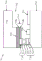
FIG. 1 is a block diagram showing a side view of a portion of a wafer level packaged infrared detector. The packaged infrared detector 10 comprises a portion of a finished (e.g., packaged) electronic device in which a lid wafer (lid wafer)100 has been sealed to a detector wafer 110. Within the sealed cavity 102 are a detector device 108 and a reference device 106. The detector device 108 and the reference device 106 may be electronic devices, as described above. In some aspects, the sealed housing 102 may be hermetically sealed. The cap wafer 100 and the detector wafer 110 may be two components that package the infrared detector 10. The detector wafer 110 may include a substrate (e.g., a silicon-based substrate) that includes any number of detector devices 108 formed thereon. In some embodiments, the number of detector devices 108 may correspond to the number of cavities 102 in the cap wafer 100.
The cap wafer 100 may serve as a cover for a plurality of different detector devices 108 and reference devices 106 formed on the substrate of the detector wafer 110. As discussed further below, the cap wafer 100 and the detector wafer 110 may be aligned such that the cap seal structure 124 is aligned with the detector seal structure 126 such that the cavity 102 is located above the detector device 108. The aligned sealing structures may be joined together to seal the detector device 108 and its corresponding reference device 106 from the surrounding environment.
The underside of the cap wafer 100 may include a barrier/getter material 104, which in certain embodiments and as described further below, may also serve as an optical shield as well as a solder barrier. In certain embodiments, the barrier/getter material 104 may chemically absorb reactive gases in a vacuum environment. The barrier/getter material 104 may be composed of a highly porous and mechanically stable composition. According to some embodiments, the barrier/getter material 104 may comprise titanium. The titanium may comprise a native oxide layer or any other treated oxide layer.
The barrier/getter material 104 may provide at least one of three functions. First, it can act as a barrier to prevent the bonding agent used to seal the cap wafer to the detector wafer from contacting one or more surfaces of the cap wafer. This blocking capability effectively prevents any metallurgical reaction between the bonding agent and the silicon of the cap wafer. For example, if the bonding agent is solder, the solder may not wet to the barrier/getter material 104. Since solder will not adhere to the barrier/getter material 104, a seal ring (discussed below) may be placed in close proximity to the array of fiducial devices 106. Furthermore, the blocking/gettering material 104 may be configured to cover only a portion of the cap wafer, and thus the blocking capability may be localized to the area at the boundary of the seal ring and/or outside of the boundary. Second, the barrier/getter material 104 may act as a getter material for removing undesired impurities in the sealed cavity 102. As used herein, the term "getter material" refers to a substance that absorbs, adsorbs, or chemically constrains one or more undesired materials or reactions with such materials as water, oxygen, hydrogen, organic vapors, and mixtures thereof. In both examples, the barrier/getter material 104 may act as a barrier between the solder material and the silicon. This barrier capability may also prevent lateral permeation of the barrier layer itself, which may degrade the integrity of the vacuum in the sealed cavity 102. In another example, a layer of material that acts as an optical shield may be present on the cover wafer. The layer of material may be composed of the same material or materials used to construct the sealing ring, so any cement that is squeezed out of the seal may also wet onto the optical shield and be drawn out of the seal. By careful placement of the barrier/getter material 104, the non-wettability of the barrier/getter material 104 will keep the extruded solder in the vicinity of the bond line and maintain the integrity of the bond. Third, the blocking/gettering material 104 may serve as an optical shield, i.e., may serve to shield the reference device 106 from incident radiation detected by the detector device 108, as discussed further below.
The lid wafer 100 may include a lid substrate 128 and a barrier/getter material 104. The cover substrate 128 may be any suitable silicon (e.g., a Czochralski (Czochralski) silicon wafer, a magnetically-confined Czochralski (Czochralski) silicon wafer, or a float zone (float zone) silicon wafer) for covering and sealing the detector device 108. In some embodiments, the lid substrate 128 may comprise a material other than silicon. According to some embodiments, the cover substrate 128 may include one or more portions that are transmissive to incident radiation of various wavelengths of infrared light (e.g., light having wavelengths between 3-14 microns) and visible light (assuming the cover substrate is not silicon). In some embodiments, the transmissive portion of the cap wafer 100 may be between about 200 and 725 microns thick. For example, in a particular embodiment, the total thickness of the cap wafer 100 may be approximately 500 and 850 microns thick. In various embodiments, the lid wafer 100 may include additional layers. For example, the cap wafer 100 may include a layer of float-zone silicon or other silicon bonded to a layer of silicon-on-insulator (SoI) material in which the cavity 102 is formed.
The lid wafer 100 may include several cavities 102 formed in a lid substrate 128. Each cavity 102 may correspond to a different detector device 108 and may be configured such that the corresponding detector device 108 is able to fit therein (e.g., the length, width, and depth of the cavity 102 may be based on the length, width, and height of the detector device 108). The depth of the cavity 102 may vary depending on the thickness of the detector device 108 and/or the desired gap size between the detector device 108 and the cover substrate 128. Although the cavities 102 may extend over the corresponding detector devices 108, they may not extend over the reference devices 106. This may allow the blocking/gettering material 104 to shield the reference device 106 from light and/or incident radiation.
The cavity 102 may be formed in the lid substrate 128 by using any of a variety of techniques performed before or after the barrier/getter material 104 is deposited on the lid substrate 128. For example, in some embodiments, the barrier/getter material 104 may be deposited first, and then the same photolithographic mask may be used to etch (e.g., using deep reactive ion etching techniques) the cavity 102 in both the barrier/getter material 104 and the lid substrate 128. As another example, and as discussed further below, the barrier/getter material 104 may be deposited after the cavity 102 has been formed in the lid substrate 128. In such embodiments, the barrier/getter material 104 may be deposited around the cavity 102, or it may be deposited everywhere and then removed from the cavity 102. Any other technique for depositing the barrier/getter material 104 to expose the silicon of the lid substrate 128 through the cavity 102 may be used.
Depending on the embodiment, the barrier/getter material 104 may be deposited on the lid substrate 128 (or a portion thereof) prior to forming the cavity 102. In some embodiments, the cavity 102 may be formed in the barrier/getter material 104 and the lid substrate 128 using the same photolithographic mask. This can reduce the number of manufacturing steps compared to using a separate mask. Using the same mask may also allow the barrier/getter material 104 to be deposited right to the edges of the cavity 102. This may reduce the amount of any internal reflections of light and/or incident radiation that can reach the reference device 106.
In some embodiments, the blocking/getter material 104 may have two or more view ports (not shown). The inspection port may provide a viewing window that may be used to visually inspect the alignment of the lid seal structure 124 and the detector seal structure 126 prior to engagement. The viewport can also be used to check alignment after bonding. The viewport can be placed at various points around the barrier/getter material 104. For example, in some embodiments, they may be disposed around the perimeter of the barrier/getter material 104. As another example, they may be disposed adjacent to a portion of the lid seal structure 124 or adjacent to the entirety of the lid seal structure 124.
In one or more embodiments, the cap seal structure 124 may be deposited directly on the barrier/getter material 104. The lid seal structure 124 may form a complete loop or ring around the cavity 102. As previously described, the barrier/getter material 104 may resist or not bond with the bonding agent used to seal the cover to the detector wafer. For example, if the bonding agent comprises solder, the barrier/getter material 104 may make it less wettable by the solder. The surface tension of the solder may help to retain the solder within the sealing structure. This may allow the distance between the inner edge of the cap seal structure 124 and the reference device 106 and the distance between the inner edge of the cap seal structure 124 and the inner edge of the barrier/getter material 104 to be reduced.
The lid seal structure 124 and the detector seal structure 126 may be two components for enclosing the detector device 108 and the reference device 106 within the cavity 102 to form a hermetic seal that encapsulates the infrared detector. In some embodiments, the chamber 102 may be in a vacuum state. The components of the sealing structure may form a closed loop of any shape around one or more components of the infrared detector. Each detector sealing structure 126 may surround a corresponding detector device 108 and its associated reference device 106. For example, if the detector wafer includes twenty detector arrays, twenty detector sealing structures may be formed. Each sealing structure may be slightly larger than the dimensions of the detector device and its associated reference device. In the illustrated embodiment, the lid seal structure 124 surrounds the cavity 102 and the detector seal structure 126 surrounds the detector device 108 and the reference device 106. As discussed further below, cement 116 may be applied to one or both of the seal structures to form a seal between the cover seal structure 124 and the detector seal structure 126.
The composition of the sealing structures 124 and 126 may include multiple layers of different metals. For example, they may include one or more of titanium Tungsten (TiW), titanium (Ti), platinum (Pt), nickel (Ni), and gold (Au). Other similar metals may be used, and one or more layers may be used. In some embodiments, the cap seal structure 124 may be formed over the barrier/getter material 104, which may act as a barrier. In such embodiments, the barrier/getter material 104 may include one or more of the layers of the cap seal structure 124. For example, the metal layer 112 may be removed from the cap seal structure 124 and replaced with the barrier/getter material 104. In some embodiments, the top layer (e.g., the layer furthest from each respective wafer) may comprise gold, or any other material to which the bonding agent is readily bonded.
The detector device 108 may include any one or more of a variety of different detectors, such as a long wave infrared detector, a short wave infrared detector, a near infrared detector, or any other detector capable of capturing images, heat, or otherwise. The type of detector device 108 used may depend on the intended application for which the infrared detector is packaged. For example, packaged infrared detectors may be used in video cameras, still image cameras, Forward Looking Infrared Systems (FLIRs), and the like. In certain embodiments, the detector device may be a plurality of detectors, such as an array of detectors or a plurality of detector arrays. The plurality of detector arrays may be independent detector arrays formed on a single substrate of the detector wafer. Each detector device may comprise a two-dimensional array of individual detectors. For example, the individual detector may comprise a microbolometer (microbolometer). Particular embodiments may include other types of infrared detectors, or other types of detectors. Each individual detector may be independently responsive to incident radiation. The size of the two-dimensional array may vary depending on the intended application. For example, in some embodiments, a two-dimensional array may include individual detectors arranged in 640 columns by 480 rows. In some embodiments, the detector device may comprise an array of microbolometer detectors, wherein each microbolometer may experience a change in resistance due to a change in temperature caused by incident radiation.
The reference device 106 may include one or more detectors, such as a detector array that may be functionally similar to the detector array used in the detector device 108. However, the number of devices in the reference device 106 may be less than the number of detectors for the detector device 108, and the reference device may be shielded from illumination and/or incident radiation. The reference device 106 may be configured to measure an ambient temperature of a substrate within the cavity 102 and/or the detector device 108 (e.g., a temperature of a substrate on which the detector device is formed). These measurements may be used to calibrate or adjust the readings produced by the detector device 108. Each detector device or detector array may include at least one reference device, or in some cases, at least two reference devices. The blocking/gettering material 104 may be used to shield the reference device 106 from light and/or incident radiation detected by the detector device 108. This may provide a more accurate measurement of the ambient temperature associated with the detectors of the detector device 108 to the reference device 106.
Depending on operational requirements, the cover substrate 128 may be substantially transmissive to light and/or incident radiation of any of a variety of different wavelengths. This may allow light and/or incident radiation to reach the detector device 108. The cavity 102 may extend over the detector device 108, but not over the reference device 106. One or more layers of barrier/getter material 104 may extend all the way to the edges of the cavity 102. In some embodiments, this may be accomplished by forming the cavity 102 in both the lid substrate 128 and the blocking/gettering material 104 using the same photolithographic mask. The reference device 106 may be shielded from illumination and/or incident radiation by the blocking/gettering material 104.
The lid wafer 100 and the detector wafer 110 may be sealed together with a bonding agent 116 deposited between the lid seal structure 124 and the detector seal structure 126. The lid seal structure 124 may include a layered metal stack of metal layers 112 and 114. In a particular embodiment, the barrier/getter material 104 may include titanium. In one or more embodiments, metal layer 112 may comprise nickel and metal layer 114 may comprise gold. The detector sealing structure 126 may include a layered metal stack of metal layers 118, 120, and 122. In some embodiments, metal layer 122 may comprise titanium, metal layer 120 may comprise nickel, and metal layer 118 may comprise gold. Other materials such as platinum may also be used. Both metal layers 114 and 118 may be made of the same material (e.g., gold). The material used may be one that readily bonds with bonding agent 116. For example, solder can easily wet to gold.
In some embodiments, the materials for bonding agent 116, metal layers 114 and 118, and barrier/getter material 104 may be selected to cooperate such that bonding agent 116 readily bonds to metal layers 114 and 118, but does not readily bond to barrier/getter material 104. For example, bonding agent 116 may comprise gold-tin solder (e.g., gold (80%) -tin (20%) solder), metal layers 114 and 118 may comprise gold, and barrier/getter material 104 may comprise titanium. Other combinations of materials may be used depending on operational or manufacturing requirements. Since bonding agent 116 can readily bond with metal layers 114 and 118, but does not readily bond with barrier/getter material 104, any bonding agent material that may spread from the sealing structure during bonding can retract into the seal due to the resistance of barrier/getter material 104 to wetting properties relative to metal layers 114 and 118.
In another aspect, fig. 2 depicts a top view of a packaged single infrared detector device. The encapsulated infrared detector 20 includes a detector device (pixel array) 208 with a blocking/gettering material 204 extending from the outer boundary of the cover to the edge of the cavity 202. In some instances, there may be little or no gap between the barrier/getter material 204 and the cavity 202. This may provide effective shielding of the reference device 206 from light and/or incident radiation. In addition, because there is no need to worry about the bonding agent adhering to the barrier/getter material 204, the sealing structures 224 and 226 may be formed on the barrier/getter material 204 at a short distance from the reference device 206. This may allow for a smaller package of incident radiation detectors.
According to yet another aspect, FIG. 3 is a block diagram of a side view of a portion of a packaged infrared detector similar to FIG. 1. The encapsulated infrared detector 30 includes a cap seal structure 324 that is formed on a cap substrate 328 prior to deposition of the barrier/getter material 304. The barrier/getter material 304 may be deposited around the perimeter of the lid seal structure 324 and may extend to the edges of the cavity 302. In the alternative, the barrier/getter material 304 may not extend to the edges of the cavity 302. The barrier/getter material 304 may be deposited all the way to just the edge of the perimeter of the sealing structure 324 or, in some cases, may actually overlap slightly with a portion of the perimeter of the sealing structure 324 to prevent contact of the bonding material with the cap wafer surface. This may be a preferred embodiment if the barrier/getter material 304 is located under the seal (rather than the metal layer 312) and has a porosity that may lead to leakage under the seal structure 324.
In another aspect, FIG. 4 shows a block diagram of a side view of a portion of an encapsulated infrared detector in which a barrier layer 430 is deposited directly onto a substrate. As used herein, the term "barrier layer" refers to a material that prevents the bonding material from interacting with the silicon surface. The barrier layer 430 may also function as a light and/or heat (e.g., infrared) barrier layer when deposited on the surface of the cover substrate 428. In some cases where the optical shield located above the reference device is built with the same metal stack as the cap seal structure 424, the bonding material that is extruded from the seal area may wet onto the optical shield and be drawn out of the bond line. If the barrier layer 430 is not wetted by the bonding material (solder), surface tension will keep the extruded solder near the bond wire and the barrier layer 430 may allow for a smaller separation between the detector sealing structure 426 and the reference device 406. In some cases, this may allow for smaller infrared detector designs (e.g., smaller die sizes), which may increase the die count of the detector wafer 410. In some embodiments, barrier layer 430 may include titanium Tungsten (TiW), which may prevent wetting of bonding materials such as solder (e.g., gold (80%) -tin (20%)). TiW may also be generally opaque in order to block light and/or incident radiation (e.g., infrared radiation). This may allow the barrier layer 430 to shield the reference device 406 from illumination and/or incident radiation. In certain embodiments, the barrier layer 430 may comprise TiW or any other suitable material that can block incident radiation and resist bonding with a bonding agent.
In various aspects, the cap seal structure 424 may be deposited onto the barrier layer 430. This configuration may allow the barrier layer 430 to comprise one of the layers that cover the sealing structure 424. One or more layers of barrier/getter material 404 may then be deposited onto the barrier layer 430 and around the perimeter of the cap seal structure 424.
In yet another aspect, fig. 5 illustrates a block diagram of a portion of the packaged infrared detector 50, wherein the first layer of blocking/gettering material 504a is deposited on the cover substrate 528. A cap seal structure 524 is then formed over the first layer of barrier/getter material 504 a. This step is followed by depositing a second layer of barrier/getter material 504b on the surface of the first layer of barrier/getter material 504a and around the perimeter of the lid sealing structure 524. In this example, the first layer of barrier/getter material 504a may be included as one of the layers of the cap seal ring 524 and may facilitate hermetic sealing of the device.
According to yet another aspect, fig. 6 is another example of a packaged device similar to fig. 4, including a barrier layer 630 deposited on the substrate, but with the difference that this step is followed by the deposition of at least one layer of barrier/getter material 604. Thus, the barrier/getter material 604 is deposited directly onto the barrier layer 630 prior to forming the cap seal 624. Both barrier layer 630 and barrier/getter material 604 may help to hermetically seal the device.
According to yet another aspect, fig. 7 illustrates a block diagram of a packaged device combining various elements of the structures shown in fig. 4 and 5. In this embodiment, the barrier layer 730 is first deposited on the cover substrate 728. Followed by the deposition of a first layer of barrier/getter material 704 a. A cap seal structure 724 is then formed over the first layer of barrier/getter material 704 a. A second layer of barrier/getter material 704a may then be deposited on the surface of the first layer of barrier/getter material 704a and around the perimeter of the lid seal structure 724.
So far, several different embodiments and features have been presented. Particular embodiments may combine one or more of these features depending on operational requirements and/or component limitations. This may allow for better adaptation of the packaged infrared detector to various user environmental requirements. Those skilled in the art will appreciate that some embodiments may include additional features. It should be noted that although the focus of the description is based on infrared detectors, other devices, such as micro-electromechanical system (MEMS) devices, may include similar features (e.g., using layers that resist bonding with bonding agents) that may benefit from the methods and systems described herein.
FIG. 8 is a flow chart illustrating two methods for performing certain embodiments of the present invention. At step 810, a substrate with a cavity is provided. As used herein, the term "substrate" refers to a base or underlying material upon which metal and/or additional materials or layers are deposited. Substrates include, but are not limited to, for example, electronic substrates, metal substrates, ceramic substrates, polymer substrates, and the like, or combinations thereof. Electronic substrates include, but are not limited to, for example, semiconductors, chips, wafers, silicon-containing substrates, and the like, or combinations thereof. Suitable substrates may generally comprise a single or primary material, or alternatively comprise two or more materials selected from, for example, metals, ceramics, polymers, and the like, or combinations thereof. Ceramics may include, for example, silicon carbide (SiC) and tantalum nitride (TaN), but are not limited to these particular materials. The polymers may include, for example, organosilane glasses (OSG), low-k dielectric materials, siloxanes, methyl silsesquioxanes, polysiloxanes, and other polymers selected from the main classes of inorganic, organic, and hybrid polymers. Therefore, the structure and composition of the substrate are not limited. For example, the materials and layers of the substrate can have any arrangement, order (e.g., sequential, hierarchical, etc.) and/or pattern so long as the is suitable for the intended application, article of manufacture, composition of matter. For example, the semiconductor substrate may comprise silicon, but may comprise, for example, sapphire in situations where radiation tolerance is important, such as military applications. The substrate may be any material that can be used as a support structure, including but not limited to the semiconductor substrates described above.
According to one or more embodiments, the substrate may include at least one cavity. As used herein, the terms "cavity" and "recess" are used interchangeably and should be given their broadest general meaning, including but not limited to a space or hollow region surrounded by something such as one or more layers or structures. In some examples, a cavity may be described as a depression or pit (depression) within the wafer material that does not actually extend through the wafer. According to yet another aspect, a substrate may have at least one cavity and a surface surrounding the at least one cavity.
In some examples, the substrate may be a lid substrate. As used herein, the terms "cap substrate," "cap wafer," and "cap wafer" are used interchangeably to refer to a wafer comprising at least one recess that is suitable for use with a device wafer comprising one or more electronic devices, such as MEMS devices. The cavity may comprise one or more layers of optically transmissive material. In this configuration, the cap wafer provides an optically transmissive window on the MEMS device. The cover substrate may be a thermally and/or optically transparent silicon wafer. In some embodiments, the cover substrate may comprise a material other than silicon.
In accordance with one or more embodiments, a sealing structure may be formed on a portion of the substrate at step 820a, or in the alternative, a sealing structure may be formed on a portion of the barrier/getter material at step 830 b. For example, the sealing structure may form a ring around the perimeter of the at least one cavity. The term "sealing structure" is intended to refer to one or more structures that may be used to form at least a portion of a seal between one or more electronic devices within an electroactive area of a substrate and ambient conditions. In various aspects, the sealing structure may be used in conjunction with a substrate that includes one or more electronic components to form an encapsulation assembly (encapsulation assembly). The encapsulation assembly may be used to substantially protect a portion or portions of the electronic component(s) from damage caused by sources external to the electronic device. In some embodiments, the cover itself or in combination with one or more other objects may form an encapsulated assembly. The encapsulation assembly may be used as a hermetically sealed package.
The sealing structure, such as the cap sealing structure formed at step 820a, may include a stack of metals including Ti or TiW, nickel, and gold. In some embodiments, such as in the combination of steps 820b and 830b, the bottom layer of the seal structure stack may include a barrier/getter material. For example, if the barrier/getter material is titanium, the bottom layer of the cap seal structure may be titanium and the remainder of the stack may comprise nickel and gold. Each lid seal structure may surround but be slightly larger than the cavity in the lid substrate and any windows formed in the barrier/getter material. The shape of the lid seal structure may correspond to the shape and size of any detector seal structure formed on the corresponding detector wafer. For example, the sealing structure on the substrate surface may form a ring around the perimeter of the cavity.
In various embodiments, at least one layer of barrier/getter material, such as titanium, may be deposited on the surface of the lid substrate at step 820 b. In the alternative, the barrier/getter material may be deposited on the surface of the lid substrate to form a ring around the perimeter of the sealing structure, as indicated in step 830 a. The barrier/getter material may be deposited on the entire surface of the substrate or may be deposited on one or more portions of the substrate, for example by using a shadow mask. In certain aspects, the barrier/getter material may be titanium, including pure titanium. In accordance with one or more embodiments, the titanium material can have a thickness in the range of about 1000 angstroms to about 10,000 angstroms. According to other embodiments, the titanium material may have a thickness greater than 10,000 angstroms. The thickness of the titanium material can be any thickness suitable for the purpose of being used as a getter for a particular application or device. The blocking/gettering material may be configured to block light and/or incident radiation to the one or more reference devices. In addition, the barrier/getter material may resist bonding with the bonding agent used to form the completed electronic device.
As used herein, the term "layer" is used interchangeably with the term "film" and refers to a coating that covers the desired area. The term is not limited by size. Layers and films may be formed by any deposition technique including vapor deposition, liquid deposition, and thermal transfer.
According to at least one aspect, vacuum evaporation or sputtering may be used to deposit at least one layer of titanium material. For example, in certain embodiments, the titanium material may be deposited under high vacuum conditions in the absence of a reactive gas. In one or more aspects, it may be desirable to remove any native oxide present on the substrate surface prior to depositing the titanium material. As will be appreciated by those skilled in the relevant art, each suitable reaction condition, including reaction atmosphere, reaction temperature, reaction duration, and preparation procedure (work procedure), may be selected based on the particular application. In various aspects, the deposition process produces a highly porous titanium material having an extremely large surface area and microstructure, i.e., a number of boundaries between individual grains or crystalline structures that make up the layer.
In various aspects, the at least one layer of titanium material can be characterized by porosity. In one or more aspects, the titanium material can be characterized as being more porous than one or more other materials used in the device. For example, the titanium material may be more porous than the underlying barrier layer. The titanium material may be porous so as to act as a getter. In some examples, the titanium material can have a porosity that can lead to leakage when it is located between the silicon substrate of the lid wafer and one or more components of the lid sealing structure. In this case, it may be advantageous to place a layer of barrier material (having a lower porosity than the titanium material) directly on the cap substrate to act as a barrier between the titanium layer and one or more components of the cap seal structure.
Referring back to fig. 8, in certain embodiments, the barrier/getter material may be activated (activated) at step 840. As used herein, the term "activation" when used in relation to a titanium material refers to any process that may be performed on the titanium material to make it useful as a getter material. For example, in certain embodiments, the titanium material may be activated by subjecting the device package to a suitable combination of temperature and time. According to certain aspects, the activation may be performed at the completion of device fabrication. In some embodiments, the device package may be hermetically sealed upon activation of the barrier/getter material. In other embodiments, the titanium material may be activated during the hermetic sealing process, i.e., during bonding or alignment of the cap wafer to the device wafer. In certain non-limiting embodiments, the titanium material may be activated by placing the material in a vacuum environment and heating it to a temperature in the range of about 200 ℃ to about 500 ℃ for a period of time in the range of about 10 minutes to about 120 minutes. The process involved in activating the at least one layer of titanium material may be performed under any conditions suitable to cause desorption of any unwanted species in the titanium material and to allow the titanium material to function as a getter and barrier as described herein. In some aspects, the titanium material may be used as a barrier layer even without activation. In other aspects, titanium materials may be used as optical shields. This function may be present with or without activation. In various aspects, activation results in a barrier/getter material having at least one of a high porosity, low granulation (granulation) and a mechanically strong structure.
In various aspects, subsequent processing may be configured to maintain the functionality of the barrier/getter material after activation, for example, such that the exposed surface of the barrier/getter material is still capable of reacting with or absorbing one or more gaseous species, thereby acting as a getter material. According to certain aspects, the particular temperature and materials used in subsequent processing steps may be specifically selected to maintain the integrity of the barrier/getter material for use as a getter material. This may include avoiding the use of one or more chemicals (i.e., reactive acids) or environments that may react with the barrier/getter material. For example, after activation, the barrier/getter material may only be exposed to a vacuum or other oxygen-free environment.
Fig. 9 also illustrates two methods for performing certain embodiments of the present invention, which are similar to the method outlined in fig. 8, except that no cavity is provided for the substrate. At step 910, a substrate, such as a lid substrate, is provided. At step 920a, a sealing structure may be formed on the substrate, or in the alternative, the sealing structure may be formed after the barrier/getter material is deposited (step 920b) at step 930 b. In step 920b, a barrier/getter material may be deposited on the lid substrate, or in the alternative, on the surface of the lid substrate to form a ring around the perimeter of the sealing structure, as indicated in step 930 a.
At step 940, one or more cavities may be formed by removing a portion of the lid substrate and/or the blocking/gettering material. For example, at least one layer of a barrier/getter material, such as a titanium material, may be deposited on the substrate, and then the at least one layer of titanium material and the substrate may be subjected to an etching process, forming a cavity in the substrate. In other examples, the lid seal ring may be deposited before or after the barrier/getter material is deposited, and then the cavity may be formed thereafter. In various embodiments, cavities or other features to be created on a substrate may be formed by using photolithographic techniques. For example, a photoresist mask may be applied to at least one layer of the barrier/getter material to define a pattern such as cavities to be etched into the substrate and barrier/getter material. In yet another example, the pattern may include a plurality of windows in the barrier/getter material and a plurality of cavities in the cover substrate. The number of windows and cavities may correspond to the number of detector arrays, both windows in the blocking/gettering material and cavities in the cover substrate may be formed using the same photoresist mask. This may help ensure that at least two dimensions of both the window in the barrier/getter material and the cavity in the lid substrate are substantially similar, and that the barrier/getter material extends right up to the edge of the cavity in the lid substrate. Using the same mask may also reduce the number of steps required to manufacture the packaged infrared detector.
The cavity may be formed by removing a portion of the barrier/getter material, a portion of the lid substrate, or both. As will be appreciated by those skilled in the art, one or more processes may be used to form the cavity, such as an etching process. In some examples, the cavity may extend through a portion of the total thickness of the cover substrate, leaving at least some of the cover substrate to cover the detector device. Activation of the barrier/getter material may be performed at step 950 after the cavities are formed, as described above.
Some of the steps illustrated in fig. 8 and 9 may be combined, modified or deleted where appropriate, and additional steps may also be added to the process flow. Additionally, steps may be performed in any suitable order without departing from the scope of particular embodiments. The steps depicted in fig. 8 and 9 are merely examples of steps performed for certain embodiments, other embodiments may use different steps arranged in a different order. For example, in some embodiments, the cavities may be formed in the lid substrate after depositing both the barrier layer and the barrier/getter material layer on the lid substrate surface. Further, the sealing structure may be formed on a combination of the barrier layer and the barrier/getter material layer, or the sealing structure may be formed on the barrier layer, the barrier/getter material layer forming a ring around the perimeter of the sealing structure. The cavity may then be formed in the cover substrate.
According to one or more embodiments, a method of fabricating an electronic device may include depositing at least one barrier layer on a surface of a substrate. In certain non-limiting embodiments, the at least one barrier layer may be titanium tungsten. In some embodiments, the barrier layer may not be bonded to, for example, a bonding agent used to seal the cap wafer to the detector wafer. In various embodiments, the barrier layer may be used to shield the one or more reference devices from incident radiation detected by the one or more detector devices. In other cases, the barrier layer may be used to shield the barrier/getter material from contamination, such as from unwanted substances in the underlying substrate.
In various embodiments, the method of manufacturing an electronic device may further include aligning a first sealing structure on the first substrate with a second sealing structure on the second substrate. In certain aspects, the first substrate may include a cap wafer and the second substrate may be a device wafer. Alignment may be performed such that at least one cavity formed on the first substrate may be configured to at least one detector device formed on the second substrate. As used herein, the term "configured," when used with respect to alignment, refers to positioning one or more features or elements of a first substrate in a position with reference to one or more features or elements of a second substrate to allow the one or more features to function properly. For example, the cavity on the first substrate may be configured such that a perimeter around the cavity may be located above and around a perimeter of the detector device. This arrangement allows light penetrating the cavity to be detected by the detector device. In yet another example, the detector sealing structure may be aligned with the lid sealing structure. In various embodiments, aligning the detector sealing structure and the lid sealing structure may allow the window in the blocking/gettering material and the cavity in the lid substrate to be aligned with the detector device. This may allow the thermal and/or light transmissive window to cover the detector device. Such an arrangement may provide protection for the detector device while still allowing light and/or incident radiation to reach the detector device. Furthermore, because the blocking/gettering material may cover the cap wafer except for the cavity portion, the blocking/gettering material may prevent a portion of the light and/or incident radiation from reaching the reference device.
According to some embodiments, the method of manufacturing an electronic device may further include bonding the first substrate to the second substrate. As used herein, the term "joined" is used interchangeably with the term "sealed" and is intended to indicate that one surface is permanently secured to another surface. Bonding may include applying a bonding agent to the lid sealing structure, the detector sealing structure, or both. The bonding agent may be any type of bonding material that may be used to seal the detector wafer to the cover wafer. For example, the bonding agent may be a solder such as gold-tin solder (e.g., gold (80%) -tin (20%) solder). In certain embodiments, the bonding agent may be such that it adheres to the detector sealing structure and the lid sealing structure, but does not adhere to or bond with the barrier/getter material. For example, in the case of solder, the bonding agent may readily wet to the detector sealing structure and the lid sealing structure, but may not wet to the blocking/gettering material. Further, in the case of using a barrier material, the barrier material may resist bonding with the bonding agent. For example, the barrier material may be a metal such as titanium, titanium tungsten, or titanium nitride that is not wettable by the molten solder.
Bonding the cap wafer to the detector wafer can create a sealed volume in which the detector device is sealed. In some embodiments where solder is used as the bonding agent, bonding the cap wafer to the detector wafer may include melting the solder to be in a liquid state. In the liquid state, the solder may spread onto the barrier/getter material. However, because the barrier/getter material does not bond with the bonding agent (e.g., solder may not readily wet the barrier/getter material), when the solder begins to cool, it may return into the sealing structure, thereby reducing or eliminating solder spreading beyond the sealing structure. This may allow the sealing structure to be closer to the reference detector array and/or the detector array.
Although specific embodiments have been described in detail, it should be understood that various other changes, substitutions, combinations, and alterations may be made hereto without departing from the spirit and scope of the present application. The particular embodiments are intended to embrace all such alterations, substitutions, variations, modifications and variations that fall within the spirit and scope of the appended claims. For example, although embodiments have been described with reference to a number of elements included in a packaged infrared detector, such as cavities, detector devices, fiducial devices, sealing structures, barriers, blocking/gettering materials, and cements, these elements may be combined, rearranged, modified, or repositioned in order to accommodate particular detection or manufacturing requirements. In addition, any of these elements may be provided as internally integrated components or externally separate components from each other, as appropriate. Particular embodiments contemplate great flexibility in the arrangement of these elements and their internal components.
Claims (11)
1. A method of manufacturing an electronic device, comprising:
providing a first substrate having at least one cavity and a surface surrounding the at least one cavity;
depositing at least one layer of barrier material on a surface of the first substrate;
depositing a solder barrier getter layer of titanium material on said at least one layer of barrier material;
forming a first seal structure on a portion of the at least one layer of barrier material to form a ring around a perimeter of the at least one cavity, wherein the solder barrier getter layer of titanium material forms a perimeter around the first seal structure such that the solder barrier getter layer of titanium material extends into the first seal structure but not into the first seal structure, the perimeter formed by the solder barrier getter layer of titanium material defining the portion of the at least one layer of barrier material on which the first seal structure is disposed;
activating the solder barrier getter layer of titanium material in a vacuum environment to act as a getter;
providing a second substrate comprising at least one device attached thereto and a second sealing structure forming a ring around a perimeter of the at least one device;
aligning the first sealing structure to the second sealing structure such that the at least one cavity of the first substrate is located over the at least one device; and
bonding the first substrate to the second substrate using solder, wherein the solder barrier getter layer prevents the solder from contacting the first substrate during bonding.
2. The method of claim 1, wherein activating comprises heating the solder barrier getter layer of titanium material to a temperature in the range of 200 ℃ to 500 ℃ for a time period in the range of 10 minutes to 120 minutes.
3. The method of claim 1, wherein depositing the solder barrier getter layer of titanium material comprises depositing the solder barrier getter layer such that a thickness of titanium material is in a range of 1000 angstroms to 10,000 angstroms.
4. The method of claim 1, wherein activating at least one solder barrier getter layer of titanium material is performed after aligning the first sealing structure to the second sealing structure.
5. The method of claim 1, wherein activating the solder barrier getter layer of titanium material is performed simultaneously with bonding the first substrate to the second substrate.
6. The method of claim 1, wherein the at least one layer of barrier material comprises titanium tungsten.
7. The method of claim 1, wherein the solder barrier getter layer of titanium material is more porous than the at least one layer of barrier material.
8. A packaged electronic device, comprising:
a first substrate having at least one cavity formed thereon and a first surface surrounding the at least one cavity;
a second substrate comprising at least one device attached thereto;
a first sealing structure disposed on a portion of the first substrate;
a second sealing structure disposed on the second substrate and bonded to the first sealing structure with solder such that the first surface faces the second substrate and the at least one cavity is located over the at least one device; and
a solder barrier comprising at least one layer of barrier material located around a perimeter of the cavity, and at least one layer of barrier getter layer of titanium material disposed on the at least one layer of barrier material and around a perimeter of the first sealing structure such that the at least one layer of barrier getter layer of titanium material extends into the first sealing structure but not into the first sealing structure, the perimeter of the first sealing structure defining a portion of the at least one layer of barrier material on which the first sealing structure is disposed, the at least one layer of barrier getter layer of titanium material having been activated to function as a getter.
9. The packaged electronic device of claim 8, wherein the at least one layer of barrier material comprises titanium tungsten.
10. The packaged electronic device of claim 8, wherein the at least one getter-blocking layer of titanium material has a thickness in the range of 1000 angstroms to 10,000 angstroms.
11. The packaged electronic device of claim 8, wherein the second substrate further comprises at least one reference device attached thereto, the at least one layer of titanium material blocking getter layer being located over the at least one reference device.
Priority Applications (1)
| Application Number | Priority Date | Filing Date | Title |
|---|---|---|---|
| CN201811055306.1A CN109231160A (en) | 2013-07-11 | 2014-07-08 | Wafer-class encapsulation solder stop object as getter |
Applications Claiming Priority (3)
| Application Number | Priority Date | Filing Date | Title |
|---|---|---|---|
| US13/939,400 | 2013-07-11 | ||
| US13/939,400 US9093444B2 (en) | 2013-07-11 | 2013-07-11 | Wafer level package solder barrier used as vacuum getter |
| PCT/US2014/045756 WO2015006327A1 (en) | 2013-07-11 | 2014-07-08 | Wafer level package solder barrier used as vacuum getter |
Related Child Applications (1)
| Application Number | Title | Priority Date | Filing Date |
|---|---|---|---|
| CN201811055306.1A Division CN109231160A (en) | 2013-07-11 | 2014-07-08 | Wafer-class encapsulation solder stop object as getter |
Publications (2)
| Publication Number | Publication Date |
|---|---|
| CN105358473A CN105358473A (en) | 2016-02-24 |
| CN105358473B true CN105358473B (en) | 2020-02-14 |
Family
ID=51293136
Family Applications (2)
| Application Number | Title | Priority Date | Filing Date |
|---|---|---|---|
| CN201480039124.9A Active CN105358473B (en) | 2013-07-11 | 2014-07-08 | Wafer level package solder barrier for use as a vacuum getter |
| CN201811055306.1A Pending CN109231160A (en) | 2013-07-11 | 2014-07-08 | Wafer-class encapsulation solder stop object as getter |
Family Applications After (1)
| Application Number | Title | Priority Date | Filing Date |
|---|---|---|---|
| CN201811055306.1A Pending CN109231160A (en) | 2013-07-11 | 2014-07-08 | Wafer-class encapsulation solder stop object as getter |
Country Status (9)
| Country | Link |
|---|---|
| US (4) | US9093444B2 (en) |
| EP (1) | EP3019441B1 (en) |
| JP (1) | JP6122220B2 (en) |
| KR (1) | KR101752107B1 (en) |
| CN (2) | CN105358473B (en) |
| CA (1) | CA2916672C (en) |
| IL (1) | IL243086A (en) |
| NO (1) | NO2944700T3 (en) |
| WO (1) | WO2015006327A1 (en) |
Families Citing this family (20)
| Publication number | Priority date | Publication date | Assignee | Title |
|---|---|---|---|---|
| FR3006236B1 (en) * | 2013-06-03 | 2016-07-29 | Commissariat Energie Atomique | DIRECT METAL BONDING PROCESS |
| US9771258B2 (en) * | 2015-06-24 | 2017-09-26 | Raytheon Company | Wafer level MEMS package including dual seal ring |
| US20170081178A1 (en) * | 2015-09-22 | 2017-03-23 | Freescale Semiconductor, Inc. | Semiconductor device package with seal structure |
| US9570321B1 (en) * | 2015-10-20 | 2017-02-14 | Raytheon Company | Use of an external getter to reduce package pressure |
| US9893027B2 (en) * | 2016-04-07 | 2018-02-13 | Nxp Usa, Inc. | Pre-plated substrate for die attachment |
| US9938134B2 (en) * | 2016-04-14 | 2018-04-10 | Taiwan Semiconductor Manufacturing Co., Ltd. | Getter electrode to improve vacuum level in a microelectromechanical systems (MEMS) device |
| US10115692B2 (en) | 2016-09-14 | 2018-10-30 | International Business Machines Corporation | Method of forming solder bumps |
| JP2018054496A (en) * | 2016-09-29 | 2018-04-05 | セイコーインスツル株式会社 | Package and Infrared Sensor |
| KR101952368B1 (en) * | 2016-11-25 | 2019-02-26 | 오승래 | Patient Specific Surgical Instrument |
| US10457549B2 (en) * | 2017-02-03 | 2019-10-29 | Taiwan Semiconductor Manfacturing Company Ltd. | Semiconductive structure and manufacturing method thereof |
| JP7408266B2 (en) * | 2017-06-14 | 2024-01-05 | 日亜化学工業株式会社 | light source device |
| CN109879240B (en) * | 2017-12-06 | 2021-11-09 | 有研工程技术研究院有限公司 | Preparation method of thick film getter material |
| US20190202684A1 (en) * | 2017-12-29 | 2019-07-04 | Texas Instruments Incorporated | Protective bondline control structure |
| FR3088319B1 (en) * | 2018-11-08 | 2020-10-30 | Ulis | HERMETIC CASE INCLUDING A GETTER, OPTOELECTRONIC COMPONENT OR MEMS DEVICE INTEGRATING SUCH A HERMETIC CASE AND ASSOCIATED MANUFACTURING PROCESS |
| CN110148571B (en) * | 2018-12-10 | 2022-03-11 | 上海欧菲尔光电技术有限公司 | Eight-inch infrared detector packaging window and preparation method thereof |
| US10968099B2 (en) * | 2018-12-28 | 2021-04-06 | Texas Instruments Incorporated | Package moisture control and leak mitigation for high vacuum sealed devices |
| CN111048472B (en) * | 2020-01-07 | 2021-12-03 | 深圳南信国际电子有限公司 | Vacuum packaging structure with coating for infrared detector |
| JP2021136413A (en) * | 2020-02-28 | 2021-09-13 | 国立研究開発法人産業技術総合研究所 | Sealing structure body and manufacturing method thereof |
| US11670616B2 (en) * | 2020-06-22 | 2023-06-06 | Epir, Inc. | Modified direct bond interconnect for FPAs |
| JP7231118B1 (en) * | 2022-04-11 | 2023-03-01 | 三菱電機株式会社 | hollow package |
Citations (6)
| Publication number | Priority date | Publication date | Assignee | Title |
|---|---|---|---|---|
| CN1320101A (en) * | 1998-07-29 | 2001-10-31 | 硅光机器公司 | Method of and apparatus for sealing an hermetic lid to a microelectronic machine |
| CN101171665A (en) * | 2005-03-18 | 2008-04-30 | 因文森斯公司 | Method of fabrication of AI/GE bonding in a wafer packaging environment and a product produced therefrom |
| CN102275863A (en) * | 2010-06-08 | 2011-12-14 | 北京广微积电科技有限公司 | Wafer-level vacuum encapsulating method for micro-electromechanical device |
| TW201234633A (en) * | 2010-10-21 | 2012-08-16 | Raytheon Co | Incident radiation detector packaging |
| CN102666368A (en) * | 2009-11-13 | 2012-09-12 | 罗伯特·博世有限公司 | Micromechanical method and corresponding assembly for bonding semiconductor substrates and correspondingly bonded semiconductor chip |
| CN102883991A (en) * | 2010-03-02 | 2013-01-16 | 森松诺尔技术有限公司 | Bonding process for sensitive micro- and nano-systems |
Family Cites Families (33)
| Publication number | Priority date | Publication date | Assignee | Title |
|---|---|---|---|---|
| US5111049A (en) * | 1990-12-21 | 1992-05-05 | Santa Barbara Research Center | Remote fired RF getter for use in metal infrared detector dewar |
| US5789859A (en) * | 1996-11-25 | 1998-08-04 | Micron Display Technology, Inc. | Field emission display with non-evaporable getter material |
| US5701008A (en) * | 1996-11-29 | 1997-12-23 | He Holdings, Inc. | Integrated infrared microlens and gas molecule getter grating in a vacuum package |
| US6499354B1 (en) | 1998-05-04 | 2002-12-31 | Integrated Sensing Systems (Issys), Inc. | Methods for prevention, reduction, and elimination of outgassing and trapped gases in micromachined devices |
| US6252229B1 (en) * | 1998-07-10 | 2001-06-26 | Boeing North American, Inc. | Sealed-cavity microstructure and microbolometer and associated fabrication methods |
| US8021976B2 (en) * | 2002-10-15 | 2011-09-20 | Megica Corporation | Method of wire bonding over active area of a semiconductor circuit |
| US6521477B1 (en) * | 2000-02-02 | 2003-02-18 | Raytheon Company | Vacuum package fabrication of integrated circuit components |
| US7315115B1 (en) * | 2000-10-27 | 2008-01-01 | Canon Kabushiki Kaisha | Light-emitting and electron-emitting devices having getter regions |
| JP2002299484A (en) * | 2001-03-29 | 2002-10-11 | Matsushita Electric Ind Co Ltd | Electronic component |
| US6853076B2 (en) * | 2001-09-21 | 2005-02-08 | Intel Corporation | Copper-containing C4 ball-limiting metallurgy stack for enhanced reliability of packaged structures and method of making same |
| US6923625B2 (en) | 2002-01-07 | 2005-08-02 | Integrated Sensing Systems, Inc. | Method of forming a reactive material and article formed thereby |
| US7276798B2 (en) * | 2002-05-23 | 2007-10-02 | Honeywell International Inc. | Integral topside vacuum package |
| WO2004001837A2 (en) | 2002-06-25 | 2003-12-31 | Unitive International Limited | Methods of forming electronic structures including conductive shunt layers and related structures |
| US6988924B2 (en) | 2003-04-14 | 2006-01-24 | Hewlett-Packard Development Company, L.P. | Method of making a getter structure |
| US20050085053A1 (en) * | 2003-10-20 | 2005-04-21 | Chien-Hua Chen | Method of activating a getter structure |
| US7427557B2 (en) * | 2004-03-10 | 2008-09-23 | Unitive International Limited | Methods of forming bumps using barrier layers as etch masks |
| US7952189B2 (en) * | 2004-05-27 | 2011-05-31 | Chang-Feng Wan | Hermetic packaging and method of manufacture and use therefore |
| US7045827B2 (en) * | 2004-06-24 | 2006-05-16 | Gallup Kendra J | Lids for wafer-scale optoelectronic packages |
| US7615833B2 (en) * | 2004-07-13 | 2009-11-10 | Avago Technologies Wireless Ip (Singapore) Pte. Ltd. | Film bulk acoustic resonator package and method of fabricating same |
| US7204737B2 (en) * | 2004-09-23 | 2007-04-17 | Temic Automotive Of North America, Inc. | Hermetically sealed microdevice with getter shield |
| KR100656192B1 (en) | 2004-11-24 | 2006-12-12 | 이병철 | Top-emission type organic light emitting display device |
| US7262412B2 (en) * | 2004-12-10 | 2007-08-28 | L-3 Communications Corporation | Optically blocked reference pixels for focal plane arrays |
| FR2883099B1 (en) * | 2005-03-14 | 2007-04-13 | Commissariat Energie Atomique | PROTECTION OF A THIN LAYER GETTER |
| US7789949B2 (en) | 2005-11-23 | 2010-09-07 | Integrated Sensing Systems, Inc. | Getter device |
| US7718965B1 (en) * | 2006-08-03 | 2010-05-18 | L-3 Communications Corporation | Microbolometer infrared detector elements and methods for forming same |
| EP2008966A3 (en) | 2007-06-27 | 2013-06-12 | Sumitomo Precision Products Co., Ltd. | MEMS device formed inside hermetic chamber having getter film |
| KR101014263B1 (en) * | 2008-09-04 | 2011-02-16 | 삼성전기주식회사 | Tactile sensor |
| US8343806B2 (en) * | 2009-03-05 | 2013-01-01 | Raytheon Company | Hermetic packaging of integrated circuit components |
| FR2946777B1 (en) | 2009-06-12 | 2011-07-22 | Commissariat Energie Atomique | DEVICE FOR DETECTING AND / OR EMITTING ELECTROMAGNETIC RADIATION AND METHOD FOR MANUFACTURING SUCH A DEVICE |
| FR2950877B1 (en) | 2009-10-07 | 2012-01-13 | Commissariat Energie Atomique | CAVITY STRUCTURE COMPRISING A BONDING INTERFACE BASED ON MATERIAL GETTER |
| FR2950876B1 (en) * | 2009-10-07 | 2012-02-10 | Commissariat Energie Atomique | METHOD FOR TREATING A GETTER MATERIAL AND METHOD FOR ENCAPSULATING SUCH A GETTER MATERIAL |
| FR2967150A1 (en) | 2010-11-09 | 2012-05-11 | Commissariat Energie Atomique | PROCESS FOR PRODUCING A SUBSTRATE WITH BURNED LAYERS OF GETTER MATERIAL |
| US20140175590A1 (en) * | 2012-12-20 | 2014-06-26 | Raytheon Company | Getter structure for wafer level vacuum packaged device |
-
2012
- 2012-10-20 NO NO15158185A patent/NO2944700T3/no unknown
-
2013
- 2013-07-11 US US13/939,400 patent/US9093444B2/en active Active
-
2014
- 2014-07-08 CN CN201480039124.9A patent/CN105358473B/en active Active
- 2014-07-08 WO PCT/US2014/045756 patent/WO2015006327A1/en active Application Filing
- 2014-07-08 JP JP2016525429A patent/JP6122220B2/en active Active
- 2014-07-08 CN CN201811055306.1A patent/CN109231160A/en active Pending
- 2014-07-08 CA CA2916672A patent/CA2916672C/en active Active
- 2014-07-08 KR KR1020167000627A patent/KR101752107B1/en active IP Right Grant
- 2014-07-08 EP EP14748016.4A patent/EP3019441B1/en active Active
-
2015
- 2015-06-10 US US14/736,042 patent/US9520332B2/en active Active
- 2015-12-22 IL IL243086A patent/IL243086A/en active IP Right Grant
-
2016
- 2016-09-20 US US15/270,145 patent/US9966320B2/en active Active
-
2018
- 2018-04-02 US US15/942,911 patent/US10262913B2/en active Active
Patent Citations (6)
| Publication number | Priority date | Publication date | Assignee | Title |
|---|---|---|---|---|
| CN1320101A (en) * | 1998-07-29 | 2001-10-31 | 硅光机器公司 | Method of and apparatus for sealing an hermetic lid to a microelectronic machine |
| CN101171665A (en) * | 2005-03-18 | 2008-04-30 | 因文森斯公司 | Method of fabrication of AI/GE bonding in a wafer packaging environment and a product produced therefrom |
| CN102666368A (en) * | 2009-11-13 | 2012-09-12 | 罗伯特·博世有限公司 | Micromechanical method and corresponding assembly for bonding semiconductor substrates and correspondingly bonded semiconductor chip |
| CN102883991A (en) * | 2010-03-02 | 2013-01-16 | 森松诺尔技术有限公司 | Bonding process for sensitive micro- and nano-systems |
| CN102275863A (en) * | 2010-06-08 | 2011-12-14 | 北京广微积电科技有限公司 | Wafer-level vacuum encapsulating method for micro-electromechanical device |
| TW201234633A (en) * | 2010-10-21 | 2012-08-16 | Raytheon Co | Incident radiation detector packaging |
Also Published As
| Publication number | Publication date |
|---|---|
| JP2016531421A (en) | 2016-10-06 |
| US20170011977A1 (en) | 2017-01-12 |
| EP3019441B1 (en) | 2017-08-23 |
| IL243086A (en) | 2017-05-29 |
| WO2015006327A1 (en) | 2015-01-15 |
| US20150014854A1 (en) | 2015-01-15 |
| EP3019441A1 (en) | 2016-05-18 |
| CA2916672A1 (en) | 2015-01-15 |
| US10262913B2 (en) | 2019-04-16 |
| US9520332B2 (en) | 2016-12-13 |
| US20150279755A1 (en) | 2015-10-01 |
| KR20160018789A (en) | 2016-02-17 |
| CA2916672C (en) | 2017-07-18 |
| US9093444B2 (en) | 2015-07-28 |
| US9966320B2 (en) | 2018-05-08 |
| JP6122220B2 (en) | 2017-04-26 |
| CN105358473A (en) | 2016-02-24 |
| KR101752107B1 (en) | 2017-06-28 |
| US20180226309A1 (en) | 2018-08-09 |
| CN109231160A (en) | 2019-01-18 |
| NO2944700T3 (en) | 2018-03-17 |
Similar Documents
| Publication | Publication Date | Title |
|---|---|---|
| CN105358473B (en) | Wafer level package solder barrier for use as a vacuum getter | |
| US8809784B2 (en) | Incident radiation detector packaging | |
| KR101931010B1 (en) | Hermetically sealed package having stress reducing layer | |
| KR102401863B1 (en) | Method for manufacturing a device comprising a hermetically sealed vacuum housing and getter | |
| US20160097681A1 (en) | Microbolometer supported by glass substrate | |
| KR102114561B1 (en) | Use of external getters to lower package pressure | |
| US9334154B2 (en) | Hermetically sealed package having stress reducing layer | |
| US20160273968A1 (en) | Sealed Infrared Imagers and Sensors | |
| US9029773B2 (en) | Sealed infrared imagers | |
| US20140267756A1 (en) | Microbolometer supported by glass substrate | |
| WO2009038686A2 (en) | Hermetic wafer level cavity package | |
| CN111044158A (en) | Method for manufacturing a device for detecting electromagnetic radiation with an improved encapsulation structure | |
| US20220283034A1 (en) | Method for Producing a Thermal Infrared Sensor Array in a Vacuum-Filled Wafer-Level Housing | |
| JP2019091931A (en) | Hermetically sealed package having stress reducing layer |
Legal Events
| Date | Code | Title | Description |
|---|---|---|---|
| C06 | Publication | ||
| PB01 | Publication | ||
| C10 | Entry into substantive examination | ||
| SE01 | Entry into force of request for substantive examination | ||
| GR01 | Patent grant | ||
| GR01 | Patent grant |