CN105164788B - Gas flow control gasket with spatially distributed gas channels - Google Patents
Gas flow control gasket with spatially distributed gas channels Download PDFInfo
- Publication number
- CN105164788B CN105164788B CN201480024290.1A CN201480024290A CN105164788B CN 105164788 B CN105164788 B CN 105164788B CN 201480024290 A CN201480024290 A CN 201480024290A CN 105164788 B CN105164788 B CN 105164788B
- Authority
- CN
- China
- Prior art keywords
- gas
- substrate
- liner
- gas passages
- liner assembly
- Prior art date
- Legal status (The legal status is an assumption and is not a legal conclusion. Google has not performed a legal analysis and makes no representation as to the accuracy of the status listed.)
- Active
Links
Images


Classifications
-
- H—ELECTRICITY
- H01—ELECTRIC ELEMENTS
- H01L—SEMICONDUCTOR DEVICES NOT COVERED BY CLASS H10
- H01L21/00—Processes or apparatus adapted for the manufacture or treatment of semiconductor or solid state devices or of parts thereof
- H01L21/67—Apparatus specially adapted for handling semiconductor or electric solid state devices during manufacture or treatment thereof; Apparatus specially adapted for handling wafers during manufacture or treatment of semiconductor or electric solid state devices or components ; Apparatus not specifically provided for elsewhere
- H01L21/67005—Apparatus not specifically provided for elsewhere
- H01L21/67011—Apparatus for manufacture or treatment
- H01L21/67098—Apparatus for thermal treatment
-
- C—CHEMISTRY; METALLURGY
- C23—COATING METALLIC MATERIAL; COATING MATERIAL WITH METALLIC MATERIAL; CHEMICAL SURFACE TREATMENT; DIFFUSION TREATMENT OF METALLIC MATERIAL; COATING BY VACUUM EVAPORATION, BY SPUTTERING, BY ION IMPLANTATION OR BY CHEMICAL VAPOUR DEPOSITION, IN GENERAL; INHIBITING CORROSION OF METALLIC MATERIAL OR INCRUSTATION IN GENERAL
- C23C—COATING METALLIC MATERIAL; COATING MATERIAL WITH METALLIC MATERIAL; SURFACE TREATMENT OF METALLIC MATERIAL BY DIFFUSION INTO THE SURFACE, BY CHEMICAL CONVERSION OR SUBSTITUTION; COATING BY VACUUM EVAPORATION, BY SPUTTERING, BY ION IMPLANTATION OR BY CHEMICAL VAPOUR DEPOSITION, IN GENERAL
- C23C16/00—Chemical coating by decomposition of gaseous compounds, without leaving reaction products of surface material in the coating, i.e. chemical vapour deposition [CVD] processes
- C23C16/44—Chemical coating by decomposition of gaseous compounds, without leaving reaction products of surface material in the coating, i.e. chemical vapour deposition [CVD] processes characterised by the method of coating
- C23C16/4401—Means for minimising impurities, e.g. dust, moisture or residual gas, in the reaction chamber
-
- C—CHEMISTRY; METALLURGY
- C23—COATING METALLIC MATERIAL; COATING MATERIAL WITH METALLIC MATERIAL; CHEMICAL SURFACE TREATMENT; DIFFUSION TREATMENT OF METALLIC MATERIAL; COATING BY VACUUM EVAPORATION, BY SPUTTERING, BY ION IMPLANTATION OR BY CHEMICAL VAPOUR DEPOSITION, IN GENERAL; INHIBITING CORROSION OF METALLIC MATERIAL OR INCRUSTATION IN GENERAL
- C23C—COATING METALLIC MATERIAL; COATING MATERIAL WITH METALLIC MATERIAL; SURFACE TREATMENT OF METALLIC MATERIAL BY DIFFUSION INTO THE SURFACE, BY CHEMICAL CONVERSION OR SUBSTITUTION; COATING BY VACUUM EVAPORATION, BY SPUTTERING, BY ION IMPLANTATION OR BY CHEMICAL VAPOUR DEPOSITION, IN GENERAL
- C23C16/00—Chemical coating by decomposition of gaseous compounds, without leaving reaction products of surface material in the coating, i.e. chemical vapour deposition [CVD] processes
- C23C16/44—Chemical coating by decomposition of gaseous compounds, without leaving reaction products of surface material in the coating, i.e. chemical vapour deposition [CVD] processes characterised by the method of coating
- C23C16/455—Chemical coating by decomposition of gaseous compounds, without leaving reaction products of surface material in the coating, i.e. chemical vapour deposition [CVD] processes characterised by the method of coating characterised by the method used for introducing gases into reaction chamber or for modifying gas flows in reaction chamber
- C23C16/45519—Inert gas curtains
-
- H—ELECTRICITY
- H01—ELECTRIC ELEMENTS
- H01L—SEMICONDUCTOR DEVICES NOT COVERED BY CLASS H10
- H01L21/00—Processes or apparatus adapted for the manufacture or treatment of semiconductor or solid state devices or of parts thereof
- H01L21/02—Manufacture or treatment of semiconductor devices or of parts thereof
- H01L21/04—Manufacture or treatment of semiconductor devices or of parts thereof the devices having at least one potential-jump barrier or surface barrier, e.g. PN junction, depletion layer or carrier concentration layer
- H01L21/18—Manufacture or treatment of semiconductor devices or of parts thereof the devices having at least one potential-jump barrier or surface barrier, e.g. PN junction, depletion layer or carrier concentration layer the devices having semiconductor bodies comprising elements of Group IV of the Periodic System or AIIIBV compounds with or without impurities, e.g. doping materials
- H01L21/30—Treatment of semiconductor bodies using processes or apparatus not provided for in groups H01L21/20 - H01L21/26
- H01L21/324—Thermal treatment for modifying the properties of semiconductor bodies, e.g. annealing, sintering
-
- H—ELECTRICITY
- H01—ELECTRIC ELEMENTS
- H01L—SEMICONDUCTOR DEVICES NOT COVERED BY CLASS H10
- H01L21/00—Processes or apparatus adapted for the manufacture or treatment of semiconductor or solid state devices or of parts thereof
- H01L21/67—Apparatus specially adapted for handling semiconductor or electric solid state devices during manufacture or treatment thereof; Apparatus specially adapted for handling wafers during manufacture or treatment of semiconductor or electric solid state devices or components ; Apparatus not specifically provided for elsewhere
- H01L21/67005—Apparatus not specifically provided for elsewhere
- H01L21/67011—Apparatus for manufacture or treatment
- H01L21/67017—Apparatus for fluid treatment
-
- H—ELECTRICITY
- H01—ELECTRIC ELEMENTS
- H01L—SEMICONDUCTOR DEVICES NOT COVERED BY CLASS H10
- H01L21/00—Processes or apparatus adapted for the manufacture or treatment of semiconductor or solid state devices or of parts thereof
- H01L21/67—Apparatus specially adapted for handling semiconductor or electric solid state devices during manufacture or treatment thereof; Apparatus specially adapted for handling wafers during manufacture or treatment of semiconductor or electric solid state devices or components ; Apparatus not specifically provided for elsewhere
- H01L21/67005—Apparatus not specifically provided for elsewhere
- H01L21/67011—Apparatus for manufacture or treatment
- H01L21/67098—Apparatus for thermal treatment
- H01L21/67115—Apparatus for thermal treatment mainly by radiation
-
- H—ELECTRICITY
- H01—ELECTRIC ELEMENTS
- H01L—SEMICONDUCTOR DEVICES NOT COVERED BY CLASS H10
- H01L21/00—Processes or apparatus adapted for the manufacture or treatment of semiconductor or solid state devices or of parts thereof
- H01L21/67—Apparatus specially adapted for handling semiconductor or electric solid state devices during manufacture or treatment thereof; Apparatus specially adapted for handling wafers during manufacture or treatment of semiconductor or electric solid state devices or components ; Apparatus not specifically provided for elsewhere
- H01L21/67005—Apparatus not specifically provided for elsewhere
- H01L21/67242—Apparatus for monitoring, sorting or marking
- H01L21/67253—Process monitoring, e.g. flow or thickness monitoring
-
- Y—GENERAL TAGGING OF NEW TECHNOLOGICAL DEVELOPMENTS; GENERAL TAGGING OF CROSS-SECTIONAL TECHNOLOGIES SPANNING OVER SEVERAL SECTIONS OF THE IPC; TECHNICAL SUBJECTS COVERED BY FORMER USPC CROSS-REFERENCE ART COLLECTIONS [XRACs] AND DIGESTS
- Y10—TECHNICAL SUBJECTS COVERED BY FORMER USPC
- Y10T—TECHNICAL SUBJECTS COVERED BY FORMER US CLASSIFICATION
- Y10T137/00—Fluid handling
- Y10T137/8593—Systems
- Y10T137/87265—Dividing into parallel flow paths with recombining
Abstract
Embodiments of the present disclosure provide a cushion assembly that includes a plurality of individually separated gas passages. The liner assembly enables the maintenance of flow parameters, such as velocity, density, direction and spatial location, across a substrate to be processed. The process gas may be specifically tailored to suit individual processes throughout the substrate to be processed using a liner assembly according to embodiments of the present disclosure.
Description
Technical Field
Embodiments of the present disclosure generally relate to an apparatus and method for processing semiconductor substrates. In particular, embodiments of the present disclosure relate to apparatus and methods for improving gas flow distribution in a processing chamber.
Background
Some processes for manufacturing semiconductor devices are performed at high temperatures, such as rapid thermal processing, epitaxial deposition, chemical vapor deposition, physical vapor deposition, electron beam curing. Typically, a substrate being processed is heated by one or more heat sources to a desired temperature in a processing chamber. The one or more heat sources are typically mounted outside the chamber body such that energy generated by the heat sources is radiated onto a substrate positioned within the chamber body. Process gases are typically supplied to the chamber from a gas inlet and are maintained in flow within the chamber body by a pumping system connected to the process chamber. The gas distribution in conventional chambers is not uniform throughout the entire processing region. For example, the gas distribution near the gas inlet is different from the gas distribution near the pumping port, and the gas distribution near the edge region is different from the gas distribution near the center region. While continuous rotation of the substrate may reduce non-uniformity of gas distribution, as the need for uniformity increases, rotation alone may not be sufficient.
Accordingly, there is a need for a thermal processing chamber with improved gas flow distribution.
Disclosure of Invention
Embodiments of the present disclosure generally provide apparatuses and methods for processing one or more substrates at high temperatures. In particular, embodiments of the present disclosure relate to apparatus and methods for distributing one or more process gases to a process chamber.
One embodiment of the present disclosure provides a liner assembly for protecting interior surfaces of a substrate processing chamber. The liner assembly includes a ring-shaped body having an outer surface sized to be received by an inner surface of a substrate processing chamber and an inner surface defining a substrate processing volume. The ring body includes a plurality of gas passages connecting the outer surface to a substrate processing volume, and each of the plurality of gas passages is designed to connect with a gas injector and is designed to regulate gas flow.
One embodiment of the present disclosure provides an apparatus for processing a substrate. The apparatus includes a chamber body forming a chamber housing (enclosure), wherein the chamber body includes: an injection opening and a gas exhaust opening formed at opposite sides; and a substrate opening formed between the injection opening and the exhaust opening. The apparatus further comprises: a gas inlet disposed in the injection opening; a substrate support disposed in the chamber housing; and a liner assembly for protecting an inner surface of the chamber body and for regulating a gas flow of the gas inlet. The liner assembly includes a ring-shaped body having an outer surface sized to be received by an inner surface of the chamber body, the inner surface of the ring-shaped body defining a substrate processing volume, the ring-shaped body including a plurality of gas passages connecting the outer surface to the substrate processing volume, and each of the plurality of gas passages is designed to be coupled to a gas injector and is designed to regulate a gas flow.
Another embodiment of the present disclosure provides a method for processing a substrate. The method comprises the following steps: the method includes directing radiant energy from a plurality of heating elements toward a housing of a substrate processing chamber and regulating a process gas flow using a plurality of gas passages formed in a liner assembly disposed in the processing chamber. The liner assembly includes a ring-shaped body having an outer surface sized to be received by an inner surface of the chamber body, the inner surface of the ring-shaped body defining a substrate processing volume, the ring-shaped body including a plurality of gas passages connecting the outer surface to the substrate processing volume, and each of the plurality of gas passages is configured to be coupled to a gas injector and configured to regulate a gas flow.
Drawings
The above-described features of the present disclosure, as well as a more particular description of the disclosure briefly summarized above, may be understood in detail by reference to the embodiments, some of which are illustrated in the appended drawings. It is to be noted, however, that the appended drawings illustrate only typical embodiments of this disclosure and are therefore not to be considered limiting of its scope, for the disclosure may admit to other equally effective embodiments.
Fig. 1A is a schematic cross-sectional side view of a processing chamber according to one embodiment of the present disclosure.
FIG. 1B is a schematic cross-sectional top view of the processing chamber of FIG. 1A.
Fig. 2A is a schematic cross-sectional side view of a cushion assembly according to one embodiment of the present disclosure.
Fig. 2B is a second schematic cross-sectional side view of the cushion assembly of fig. 2A.
FIG. 3 is a partial cross-sectional side view of a cushion assembly according to one embodiment of the present disclosure.
FIG. 4 is a partial cross-sectional side view of a cushion assembly according to one embodiment of the present disclosure.
Fig. 5A is a partial cross-sectional side view of a cushion assembly according to one embodiment of the present disclosure.
Fig. 5B is a schematic top view of the cushion assembly of fig. 5A.
Fig. 5C is a schematic partial top view of a cushion assembly according to another embodiment of the present disclosure.
To facilitate understanding, identical reference numerals have been used, where possible, to designate identical elements that are common to the figures. It is contemplated that elements and features of one embodiment may be beneficially incorporated in other embodiments without further recitation.
Detailed Description
In the following description, for purposes of explanation, numerous specific details are set forth in order to provide a thorough understanding of the present disclosure. In some instances, well-known structures and devices are not shown in detail, but are shown in block form in order to avoid obscuring the present disclosure. These embodiments are described in sufficient detail to enable those skilled in the art to practice the disclosure, and it is to be understood that other embodiments may be utilized and that logical, mechanical, electrical and other changes may be made without departing from the scope of the present disclosure.
Embodiments of the present disclosure provide a liner assembly having a plurality of individually separated gas passages. The liner assembly enables tunability of flow parameters, such as velocity, density, direction, and spatial location, across a substrate to be processed. The process gas may be specifically tailored across the substrate to be processed to be suitable for each individual process using a liner assembly according to embodiments of the present disclosure. The gasket assembly according to the embodiments of the present disclosure has an advantage of minimizing a pressure drop in a gas injection path more than a conventional gasket. One embodiment of the present disclosure includes a liner assembly having angled or shortened flow channels to reduce pressure drop. Another advantage of a gasket assembly according to the present disclosure is that it provides adjusted and/or varied flow continuity (flow continuity) in the flow path. In one embodiment, the liner assembly may include a plurality of gas passages having different dimensions, thereby providing varying flow conductance through each of the plurality of gas passages. The spatial distribution of the plurality of gas passages in the liner assembly may also be designed to achieve a regulated gas flow in the processing chamber.
A cushion assembly according to embodiments of the present disclosure may have another advantage: preventing the multiple process gases from mixing before reaching the vicinity of the substrate to be processed. Furthermore, the gasket assembly according to the embodiment of the present disclosure also has an advantage of being able to be manufactured using a direct and simple method, such as by gun drilling (gun drilling), diffusion bonding, and using a welded plug (welded plug).
Fig. 1A shows a schematic cross-sectional view of a processing chamber 100 according to one embodiment of the present disclosure. Fig. 1B is a schematic cross-sectional top view of the processing chamber 100. The processing chamber 100 may be used to process one or more substrates, including depositing materials on the upper surface 116 of the substrate 108. The process chamber 100 may include an array of radiant heating lamps 102, the radiant heating lamps 102 being used to heat, among other things, a backside 104 of a substrate support 106 disposed within the process chamber 100. In some embodiments, an array of radiant heating lamps 102 may be disposed above an upper dome 128. The substrate support 106 may be a disk-shaped substrate support 106 without a central opening, as shown. Alternatively, the substrate support 106 may be an annular substrate support that supports the substrate from an edge thereof to facilitate exposure of the substrate to thermal radiation from the plurality of radiant heating lamps 102.
The substrate support 106 is positioned within the processing chamber 100 between the upper dome 128 and the lower dome 114. The substrate ring 136 may be disposed between the upper and lower arches 128, 114. The upper dome 128, the lower dome 114, and the base ring 136 generally define an interior region of the processing chamber 100. A substrate 108 (not drawn to scale) may be brought into the processing chamber 100 through the load port 103 and positioned on the substrate support 106, as shown in figure 1B.
In fig. 1A, the substrate support 106 is shown in a processing position. The substrate support 106 may be vertically traversed (translated) to a loading position below the processing position to allow the lift pins 105 to contact the lower arch 114, pass through the substrate support 106 and the holes in the central shaft 132, and lift the substrate 108 from the substrate support 106. When the substrate support 106 is in the processing position, the substrate support 106 divides the internal volume of the processing chamber 100 into a process gas region 156 and a purge gas (purge gas) region 158, the process gas region 156 being located above the substrate support 106 and the purge gas region 158 being located below the substrate support 106. The substrate support 106 is rotated by the central shaft 132 during processing to minimize thermal effects and spatial irregularities in the process gas flow within the processing chamber 100, thereby facilitating uniform processing of the substrate 108. The substrate support 106 is supported by a central shaft 132, which central shaft 132 moves the substrate 108 up and down along a direction 134 during loading and unloading, and in some examples moves the substrate 108 up and down along the direction 134 during processing of the substrate 108. The substrate support 106 may be formed of silicon carbide or graphite coated with silicon carbide to absorb radiant energy from the radiant heating lamps 102 and conduct the radiant energy to the substrate 108.
Generally, the central window portion of the upper dome 128 and the bottom of the lower dome 114 are formed of an optically transparent material, such as quartz. One or more lamps, such as an array of radiant heating lamps 102, may be disposed below the lower dome 114 and adjacent to the lower dome 114 in a prescribed manner about the central axis 132 to independently control the temperature at various regions of the substrate 108 as process gases pass therethrough to facilitate deposition of material onto the upper surface 116 of the substrate 108. Although not discussed in detail herein, the deposition material may include gallium arsenide, gallium nitride, or aluminum gallium nitride.
The radiant heating lamp 102 may include a bulb 141, the bulb 141 configured to heat the substrate 108 to a temperature in a range of about 200 degrees celsius to about 1600 degrees celsius. Each radiant heating lamp 102 is coupled to a power distribution board (not shown) through which power is supplied to each radiant heating lamp 102. The radiant heating lamps 102 may be arranged within a lamp head 145, the lamp head 145 having a lamp receiving opening. The lamp head 145 may be cooled during or after processing by, for example, a cooling fluid introduced into channels 149 between the radiant heating lamps 102. In one embodiment, the channel 149 in the lamp head 145 may be used to conductively and radiatively cool the lower dome 104, in part due to the close proximity of the lamp head 145 to the lower dome 104. In one embodiment, lamp head 145 may also cool the lamp walls and the walls of the reflector (not shown) around the lamp. Alternatively, the lower dome 104 may be convectively cooled as is known in the art. Depending on the application, the lamp head 145 may or may not be in contact with the lower dome 114.
A circular shield 167 may optionally be disposed around the substrate support 106. The shield 167 prevents or minimizes heat/light noise leakage from the radiant heating lamps 102 to the device side 116 of the substrate 108 while providing a pre-heat zone for the process gas. The shield 167 may be made of Chemical Vapor Deposition (CVD) SiC, sintered graphite coated with SiC, grown SiC, opaque quartz, coated quartz, or any similarly suitable material that is resistant to chemical damage by process and purge gases.
The liner assembly 163 may be positioned in the processing chamber 100. In one embodiment, the liner assembly 163 may surround a circular shield 167. The liner assembly 163 is sized to nest (nested) within the inner periphery of the base ring 136 or be surrounded by the inner periphery of the base ring 136. The liner assembly 163 isolates the process volume (i.e., the process gas region 156 and the purge gas region 158) from the metal walls of the processing chamber 100. For example, from the metal wall of the substrate ring 136. These metal walls may react with the precursors and cause contamination in the processing volume. Although the pad assembly 163 is shown as a unitary body, the pad assembly 163 may include one or more pads, as will be discussed below. In accordance with an embodiment of the present disclosure, the liner assembly 163 includes a plurality of gas channels 190, the gas channels 190 for injecting one or more process gases into the process gas region 156. The liner assembly 163 may also include a plurality of gas channels 192, the gas channels 192 for injecting one or more gases into the purge gas region 158.
The optical pyrometer 118 may be positioned outside the upper dome 128 to measure the temperature of the substrate 108. As a result of backside heating of the substrate from the substrate support 106, the substrate support can be temperature measured/controlled using the optical pyrometer 118. Such temperature measurements by the optical pyrometer 118 may also be made on the substrate device side (e.g., the upper surface 116) having an unknown emissivity, since heating the substrate backside 110 in this manner is emissivity independent. Thus, the optical pyrometer 118 may detect radiation from the substrate 108 with a very small amount of background radiation (background radiation) from the radiant heating lamps 102 reaching the optical pyrometer directly, thereby obtaining an accurate temperature measurement of the substrate 108.
One or more process gases from a process gas supply 172 may be introduced into the process gas region 156 through a process gas inlet 174, the process gas inlet 174 being disposed in a sidewall of the substrate ring 136. The process gas inlet 174 may include one or more gas injectors 196 (shown in fig. 1B) to deliver one or more separate gas flows. The process gas inlet 174 may be configured to provide separate gas flows having different parameters, such as velocity, density, or composition. Each of the one or more gas injectors 196 of the process gas inlet 174 is connected with one of a plurality of gas passages 190, the gas passages 190 being formed through the liner assembly 163. The plurality of gas passages 190 are configured to direct the process gas in a generally radially inward direction. Each of the plurality of gas passages 190 may be used to adjust one or more parameters of the process gas from the process gas inlet 174, such as velocity, density, direction, and position. The plurality of gas passages 190 condition one or more process gases from the process gas inlets 174 prior to directing the one or more process gases from the process gas inlets 174 to the process gas region 156 for processing.
During processing, the substrate support 106 may be in a processing position as shown in figure 1A. In the processing position, the substrate 108 is adjacent to the process gas inlet 174 and at about the same height as the process gas inlet 174, such that the process gas flows in a laminar flow over the upper surface 116 of the substrate 108 up and around the flow path 173. The process gases exit the process gas region 156 (along the flow path 175) through an exhaust opening 194 and a gas outlet 178, the exhaust opening 194 being formed through the liner assembly 163, and the gas outlet 178 being located on the opposite side of the processing chamber 100 from the process gas inlet 174. Removal of the process gas through the gas outlet 178 may be by means of a vacuum pump 180, the vacuum pump 180 being coupled to the gas outlet 178. Because the process gas inlet 174 and the gas outlet 178 are aligned and disposed at about the same height as one another, it is believed that such a parallel arrangement of the gas inlet 174 and the gas outlet 178, in combination with the relatively flat upper dome 128, will enable a substantially planar, uniform gas flow across the substrate 108. Further radial uniformity may be provided by rotating the substrate 108 through the substrate support 106.
Similarly, a purge gas may be supplied by a purge gas source 162 to the purge gas region 158 through an optional purge gas inlet 164 (or through a process gas inlet 174 disposed in a sidewall of the substrate ring 136), and then through a plurality of gas channels 192 formed in the liner assembly 163. The purge gas inlet 164 is disposed at a lower elevation than the process gas inlet 174. If a circular shield 167 is used, the circular shield 167 may be disposed between the process gas inlet 174 and the purge gas inlet 164. In either example, the purge gas inlet 164 is configured to direct the purge gas in a generally radially inward direction. During the film formation process, the substrate support 106 may be positioned in a position such that the purge gas flows in a laminar flow across the backside 104 of the substrate support 106 down and around the flow path 165. Without being bound by any particular theory, it is believed that the flow of the purge gas prevents or substantially avoids the flow of the process gas from entering the purge gas region 158, or reduces the diffusion of the process gas into the purge gas region 158 (i.e., the region below the substrate support 106). The purge gas exits the purge gas region 158 (along flow path 166) and is exhausted from the processing chamber 100 through a gas outlet 178, the gas outlet 178 being located on an opposite side of the processing chamber 100 from the purge gas inlet 164.
Similarly, during the purge process, the substrate support 106 may be in a raised position such that the purge gas is laterally flowed across the backside 104 of the substrate support 106.
Fig. 1B shows the flow path from the process gas inlet 174 to the gas outlet 178. A plurality of gas passages 190 may be distributed along a portion of the liner assembly 163 to direct the flow paths 173 in a substantially parallel manner. The number, size, and location of each of the gas channels 190 may be arranged according to achieving a target flow pattern (flow pattern). The exhaust openings 194 may be wide openings formed through the liner assembly 163 and located on opposite sides of the plurality of gas passages 190.
It should be understood by those of ordinary skill in the art that the plurality of gas passages 190, 192 are shown for illustration only. The location, size, and number of gas inlets or outlets, etc., may be adjusted to further assist in the uniform deposition of material on the substrate 108. Exemplary embodiments of a cushion assembly according to embodiments of the present disclosure are described below.
Fig. 2A is a schematic cross-sectional side view of a cushion assembly 200 according to one embodiment of the present disclosure. The cushion assembly 200 may include a lower cushion 210 and an upper cushion 220, the upper cushion 220 being disposed above the lower cushion 210. A plurality of gas channels 202 may be formed in the lower liner 210. The upper liner 220 may include a plurality of flow guides 222, the flow guides 222 being aligned with the plurality of gas channels 202. Each of the plurality of flow guides 222 is formed to direct a gas flow from the corresponding gas channel 202 to the process gas region 156.
The lower liner 210 may have an annular body 212. The annular body 212 has an outer surface 214 and an inner surface 216, the outer surface 214 of the annular body being adapted to face the inner surface of the substrate ring 136, and the inner surface 216 of the annular body facing the substrate 108 to be processed. The lower liner 210 has an upper surface 218 that faces the upper liner 220. A plurality of gas passages 202 and exhaust openings 204 are formed through opposite sides of the annular body 212. In one embodiment, the substrate opening 206 is formed through the annular body 212 and between the plurality of channels 202 and the exhaust opening 204.
Each of the plurality of gas passages 202 may include a horizontal portion 202a and a vertical portion 202b connected to each other. The horizontal portion 202a may be formed by drilling a blind hole from the outer surface 214. Vertical portion 202b may be formed by drilling a blind hole from upper surface 218 to connect with horizontal portion 202 a.
The upper liner 220 includes an annular body 228, the annular body 228 having a radially inwardly extending lip 226. The lip 226 defines the central opening 224. The lip 226 is positioned away from the lower liner 210. The annular body 228 has a curved inner surface 230, the curved inner surface 230 facing the lower liner 210. The plurality of flow guides 222 may be formed in the inner surface 230 to direct the flow of gas for the gas channel 202. The geometry of the flow guide 222 redirects the airflow to achieve the target flow path. The flow path 232 is schematically depicted in fig. 2A.
Fig. 2B is a second schematic cross-sectional side view of the cushion assembly 200 showing the distribution of the gas channels 202 and flow guides 222, according to one embodiment of the present disclosure.
The upper and lower liners 220 and 210 may be formed of a material compatible with the chemical conditions (chemistries) of the process. In one embodiment, the upper and lower liners 220, 210 may be formed of quartz. The plurality of gas passages 202 may be formed by gun-drilled holes.
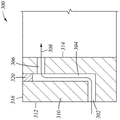
Fig. 3 is a partial cross-sectional side view of a cushion assembly 300 according to one embodiment of the present disclosure. The liner assembly 300 includes an annular body 310, the annular body 310 having an outer surface 312, an inner surface 314, and an upper surface 316. The annular body 310 defines a plurality of flow paths 308, the flow paths 308 connecting the outer surface 312 and the inner surface 314. In one embodiment, each of the plurality of flow paths 308 includes three channels 302, 304, 306 formed by drilling blind holes from an outer surface 312, an inner surface 314, and an upper surface 316, respectively. A plurality of inserts 320 may be disposed in each of the channels 304 from the upper surface 316.
Fig. 4 is a partial cross-sectional side view of a cushion assembly 400 according to one embodiment of the present disclosure. The liner assembly 400 is similar to the liner assembly 300 except that there is a cover ring 420, the cover ring 420 having a plurality of protrusions 422 for plugging the channel 304.
Fig. 5A is a partial cross-sectional side view of a cushion assembly 500 according to one embodiment of the present disclosure. Fig. 5B is a schematic top view of the cushion assembly 500. The liner assembly 500 includes a liner body 520 and an injection ring 510. The liner body 520 has an annular body with an outer surface 522 and an inner surface 524. The injection ring 510 is attached to an inner surface 524 of the annular liner body 520. The annular liner body 520 includes a plurality of horizontal channels 526, the horizontal channels 526 connecting with a respective one of a plurality of sloped channels 528. The horizontal channel 526 may be formed by drilling a blind hole from the upper surface 522, and the angled channel 528 may be formed by drilling an angled blind hole from the inner surface 524 to connect with the horizontal channel 526. The injection ring 510 includes a plurality of horizontal channels 512, the horizontal channels 512 being aligned with a plurality of slanted channels 528. These inclined channels 528 direct the airflow upward with reduced resistance. The injection ring 510 allows for easy fabrication of the angled channels 528 in the flow path.
Fig. 5C is a schematic partial top view of a cushion assembly 530 according to another embodiment of the present disclosure. The cushion assembly 530 is similar to the cushion assembly 500 except that the cushion assembly 530 includes a plurality of discrete injection blocks 532, the injection blocks 532 having horizontal channels 534 formed in the injection blocks 532.
While the foregoing is directed to embodiments of the present disclosure, other and further embodiments of the disclosure may be devised without departing from the basic scope thereof, and the scope thereof is determined by the claims that follow.
Claims (10)
1. A liner assembly for protecting interior surfaces of a substrate processing chamber having a plurality of gas injectors, the liner assembly comprising:
a ring body having an outer surface sized to be received by the inner surface of the substrate processing chamber and an inner surface defining a substrate processing volume, wherein the ring body includes a plurality of gas passages formed therethrough, wherein the plurality of gas passages connect the outer surface to the substrate processing volume and the plurality of gas passages are spaced apart to align with the plurality of gas injectors; and
an upper liner disposed above the annular body, wherein the upper liner includes a plurality of flow guides aligned with the plurality of gas passages.
2. The liner assembly of claim 1, wherein each of the plurality of gas channels comprises a sloped channel.
3. The liner assembly of claim 1, wherein each of the plurality of gas passages includes a horizontal portion and a vertical portion, the horizontal portion being open to the outer surface of the annular body, the vertical portion having an upper end and a lower end, the upper end being open to an upper surface of the annular body, the lower end being connected to the horizontal portion, and the upper end of the vertical portion being connected to a respective one of the plurality of flow guides.
4. The liner assembly of claim 3, wherein each flow guide has a curved upper surface.
5. The liner assembly of claim 4, wherein the upper liner has an inwardly extending lip.
6. An apparatus for processing a substrate, comprising:
a chamber body, wherein the chamber body encloses a chamber housing, an injection opening and an exhaust opening are formed in opposing sides of the chamber body, and a substrate opening is formed between the injection opening and the exhaust opening;
a gas inlet disposed in the injection opening, wherein the gas inlet comprises a plurality of gas injectors;
a substrate support disposed in the chamber housing; and
a liner assembly positioned to protect an inner surface of the chamber body and to regulate gas flow of the gas inlet, wherein the liner assembly comprises a ring-shaped body having an outer surface sized to be received by the inner surface of the chamber body and an inner surface defining a substrate processing volume, the ring-shaped body comprising a plurality of gas passages formed therethrough, wherein the plurality of gas passages connect the outer surface to the substrate processing volume and the plurality of gas passages are spaced apart to align with the plurality of gas injectors, and wherein the liner assembly further comprises an upper liner disposed over the ring-shaped body, wherein the upper liner comprises a plurality of flow guides, the plurality of flow guides are aligned with the plurality of gas passages in the annular body.
7. The apparatus of claim 6, wherein each of the plurality of gas passages of the liner assembly comprises a sloped channel.
8. The apparatus of claim 6, wherein each of the plurality of gas passages comprises a first horizontal portion open to the outer surface of the ring body and a vertical portion having an upper end open to an upper surface of the ring body and a lower end connected to the first horizontal portion.
9. A method for processing a substrate, comprising:
directing radiant energy from a plurality of heating elements to a housing of a substrate processing chamber; and
regulating a flow of a process gas using a plurality of gas passages formed in a liner assembly disposed in the substrate processing chamber having a plurality of gas injectors, wherein the liner assembly comprises an annular body having an outer surface sized to be received by an inner surface of a chamber body of the substrate processing chamber and an inner surface defining a substrate processing volume, the annular body comprising a plurality of gas passages formed therethrough, wherein the plurality of gas passages connect the outer surface to the substrate processing volume and each of the plurality of gas passages is designed to connect with the plurality of gas injectors and regulate the flow of the process gas, and wherein the liner assembly further comprises an upper liner, the upper liner is disposed above the annular body, wherein the upper liner includes a plurality of flow guides that are aligned with the plurality of gas passages in the annular body.
10. The method of claim 9, wherein adjusting the flow of process gas comprises: the airflow is directed through a plurality of angled channels.
Priority Applications (2)
| Application Number | Priority Date | Filing Date | Title |
|---|---|---|---|
| CN201710953411.6A CN107833848B (en) | 2013-04-30 | 2014-04-21 | Gas flow control gasket with spatially distributed gas channels |
| CN202010034452.7A CN111211074B (en) | 2013-04-30 | 2014-04-21 | Gas flow control liner with spatially distributed gas passages |
Applications Claiming Priority (3)
| Application Number | Priority Date | Filing Date | Title |
|---|---|---|---|
| US201361817691P | 2013-04-30 | 2013-04-30 | |
| US61/817,691 | 2013-04-30 | ||
| PCT/US2014/034785 WO2014179093A1 (en) | 2013-04-30 | 2014-04-21 | Flow controlled liner having spatially distributed gas passages |
Related Child Applications (2)
| Application Number | Title | Priority Date | Filing Date |
|---|---|---|---|
| CN201710953411.6A Division CN107833848B (en) | 2013-04-30 | 2014-04-21 | Gas flow control gasket with spatially distributed gas channels |
| CN202010034452.7A Division CN111211074B (en) | 2013-04-30 | 2014-04-21 | Gas flow control liner with spatially distributed gas passages |
Publications (2)
| Publication Number | Publication Date |
|---|---|
| CN105164788A CN105164788A (en) | 2015-12-16 |
| CN105164788B true CN105164788B (en) | 2020-02-14 |
Family
ID=51789571
Family Applications (3)
| Application Number | Title | Priority Date | Filing Date |
|---|---|---|---|
| CN201480024290.1A Active CN105164788B (en) | 2013-04-30 | 2014-04-21 | Gas flow control gasket with spatially distributed gas channels |
| CN202010034452.7A Active CN111211074B (en) | 2013-04-30 | 2014-04-21 | Gas flow control liner with spatially distributed gas passages |
| CN201710953411.6A Active CN107833848B (en) | 2013-04-30 | 2014-04-21 | Gas flow control gasket with spatially distributed gas channels |
Family Applications After (2)
| Application Number | Title | Priority Date | Filing Date |
|---|---|---|---|
| CN202010034452.7A Active CN111211074B (en) | 2013-04-30 | 2014-04-21 | Gas flow control liner with spatially distributed gas passages |
| CN201710953411.6A Active CN107833848B (en) | 2013-04-30 | 2014-04-21 | Gas flow control gasket with spatially distributed gas channels |
Country Status (6)
| Country | Link |
|---|---|
| US (3) | US9553002B2 (en) |
| JP (1) | JP6368773B2 (en) |
| KR (2) | KR20160003831A (en) |
| CN (3) | CN105164788B (en) |
| TW (2) | TWI679299B (en) |
| WO (1) | WO2014179093A1 (en) |
Families Citing this family (37)
| Publication number | Priority date | Publication date | Assignee | Title |
|---|---|---|---|---|
| KR101884003B1 (en) * | 2011-03-22 | 2018-07-31 | 어플라이드 머티어리얼스, 인코포레이티드 | Liner assembly for chemical vapor deposition chamber |
| US9512520B2 (en) * | 2011-04-25 | 2016-12-06 | Applied Materials, Inc. | Semiconductor substrate processing system |
| US20140116336A1 (en) * | 2012-10-26 | 2014-05-01 | Applied Materials, Inc. | Substrate process chamber exhaust |
| WO2014179093A1 (en) | 2013-04-30 | 2014-11-06 | Applied Materials, Inc. | Flow controlled liner having spatially distributed gas passages |
| US11414759B2 (en) * | 2013-11-29 | 2022-08-16 | Taiwan Semiconductor Manufacturing Co., Ltd | Mechanisms for supplying process gas into wafer process apparatus |
| US20150184292A1 (en) * | 2013-12-30 | 2015-07-02 | Lam Research Corporation | Systems and methods for preventing mixing of two gas streams in a processing chamber |
| WO2016153716A1 (en) * | 2015-03-20 | 2016-09-29 | Applied Materials, Inc. | An atomic layer process chamber for 3d conformal processing |
| US10203604B2 (en) | 2015-11-30 | 2019-02-12 | Applied Materials, Inc. | Method and apparatus for post exposure processing of photoresist wafers |
| US11150140B2 (en) * | 2016-02-02 | 2021-10-19 | Kla Corporation | Instrumented substrate apparatus for acquiring measurement parameters in high temperature process applications |
| US10260149B2 (en) * | 2016-04-28 | 2019-04-16 | Applied Materials, Inc. | Side inject nozzle design for processing chamber |
| US11397385B2 (en) | 2016-06-17 | 2022-07-26 | Taiwan Semiconductor Manufacturing Company, Ltd | Apparatus and a method of forming a particle shield |
| US10168626B2 (en) * | 2016-06-17 | 2019-01-01 | Taiwan Semiconductor Manufacturing Company, Ltd. | Apparatus and a method of forming a particle shield |
| US10788764B2 (en) | 2016-06-17 | 2020-09-29 | Taiwan Semiconductor Manufacturing Company, Ltd. | Apparatus and a method of forming a particle shield |
| US9958782B2 (en) | 2016-06-29 | 2018-05-01 | Applied Materials, Inc. | Apparatus for post exposure bake |
| USD842259S1 (en) | 2017-04-28 | 2019-03-05 | Applied Materials, Inc. | Plasma chamber liner |
| USD837754S1 (en) | 2017-04-28 | 2019-01-08 | Applied Materials, Inc. | Plasma chamber liner |
| USD838681S1 (en) | 2017-04-28 | 2019-01-22 | Applied Materials, Inc. | Plasma chamber liner |
| USD875054S1 (en) * | 2017-04-28 | 2020-02-11 | Applied Materials, Inc. | Plasma connector liner |
| USD875053S1 (en) * | 2017-04-28 | 2020-02-11 | Applied Materials, Inc. | Plasma connector liner |
| USD875055S1 (en) * | 2017-04-28 | 2020-02-11 | Applied Materials, Inc. | Plasma connector liner |
| KR20190137935A (en) * | 2017-05-01 | 2019-12-11 | 어플라이드 머티어리얼스, 인코포레이티드 | High Pressure Annealing Chamber with Vacuum Isolation and Pre-Processing Environment |
| JP6837911B2 (en) * | 2017-05-17 | 2021-03-03 | 株式会社Screenホールディングス | Heat treatment equipment |
| US11004722B2 (en) * | 2017-07-20 | 2021-05-11 | Applied Materials, Inc. | Lift pin assembly |
| KR102081704B1 (en) * | 2018-02-05 | 2020-02-27 | 세메스 주식회사 | Apparatus for treating substrate |
| CN214848503U (en) | 2018-08-29 | 2021-11-23 | 应用材料公司 | Implanter apparatus, substrate processing apparatus and structure embodied in machine-readable medium |
| US11486038B2 (en) | 2019-01-30 | 2022-11-01 | Applied Materials, Inc. | Asymmetric injection for better wafer uniformity |
| US10995419B2 (en) * | 2019-04-16 | 2021-05-04 | Applied Materials, Inc. | Methods and apparatus for gallium nitride deposition |
| US11560623B2 (en) * | 2019-05-15 | 2023-01-24 | Applied Materials, Inc. | Methods of reducing chamber residues |
| US11032945B2 (en) * | 2019-07-12 | 2021-06-08 | Applied Materials, Inc. | Heat shield assembly for an epitaxy chamber |
| US11952660B2 (en) * | 2019-07-29 | 2024-04-09 | Applied Materials, Inc. | Semiconductor processing chambers and methods for cleaning the same |
| KR20220147673A (en) * | 2020-03-02 | 2022-11-03 | 램 리써치 코포레이션 | Adapter plate for attaching turbo pumps to process modules |
| JP7462763B2 (en) | 2020-04-20 | 2024-04-05 | アプライド マテリアルズ インコーポレイテッド | MULTI-THERMAL CVD CHAMBER WITH SHARED SUPPLY AND EXHAUST SYSTEM - Patent application |
| CN112002660B (en) * | 2020-08-27 | 2024-01-19 | 南京国盛电子有限公司 | Semiconductor processing device, processing method and application |
| US20220195617A1 (en) * | 2020-12-22 | 2022-06-23 | Applied Materials, Inc. | Multi-layer epi chamber body |
| CN112768384B (en) * | 2021-01-26 | 2024-02-27 | 西安奕斯伟材料科技股份有限公司 | Preheating ring and wafer epitaxial growth equipment |
| US11781212B2 (en) * | 2021-04-07 | 2023-10-10 | Applied Material, Inc. | Overlap susceptor and preheat ring |
| EP4337814A1 (en) * | 2021-05-11 | 2024-03-20 | Applied Materials, Inc. | Gas injector for epitaxy and cvd chamber |
Citations (1)
| Publication number | Priority date | Publication date | Assignee | Title |
|---|---|---|---|---|
| CN101681833A (en) * | 2007-06-14 | 2010-03-24 | 东京毅力科创株式会社 | Micro wave plasma processing device, micro wave plasma processing method, and micro wave transmitting plate |
Family Cites Families (42)
| Publication number | Priority date | Publication date | Assignee | Title |
|---|---|---|---|---|
| US4142004A (en) * | 1976-01-22 | 1979-02-27 | Bell Telephone Laboratories, Incorporated | Method of coating semiconductor substrates |
| US4223048A (en) * | 1978-08-07 | 1980-09-16 | Pacific Western Systems | Plasma enhanced chemical vapor processing of semiconductive wafers |
| US5269847A (en) | 1990-08-23 | 1993-12-14 | Applied Materials, Inc. | Variable rate distribution gas flow reaction chamber |
| US5433780A (en) * | 1992-11-20 | 1995-07-18 | Tokyo Electron Limited | Vacuum processing apparatus and exhaust system that prevents particle contamination |
| US5916369A (en) | 1995-06-07 | 1999-06-29 | Applied Materials, Inc. | Gas inlets for wafer processing chamber |
| US6500734B2 (en) * | 1993-07-30 | 2002-12-31 | Applied Materials, Inc. | Gas inlets for wafer processing chamber |
| JP3243125B2 (en) * | 1994-06-27 | 2002-01-07 | 東京エレクトロン株式会社 | Processing equipment |
| KR19990002605A (en) | 1997-06-20 | 1999-01-15 | 이형도 | Intermittent structure of flexible circuit board for brushless motor |
| KR19990002605U (en) * | 1997-06-27 | 1999-01-25 | 김영환 | Cylinder inner wall protection cylinder |
| US6486081B1 (en) * | 1998-11-13 | 2002-11-26 | Applied Materials, Inc. | Gas distribution system for a CVD processing chamber |
| FI114855B (en) * | 1999-07-09 | 2005-01-14 | Outokumpu Oy | A method of plugging a hole and a heat sink made by the method |
| JP2002001100A (en) * | 2000-06-22 | 2002-01-08 | Mitsubishi Heavy Ind Ltd | Plasma treatment apparatus |
| JP2002100570A (en) * | 2000-09-22 | 2002-04-05 | Komatsu Electronic Metals Co Ltd | Single wafer vapor phase epitaxial growth system |
| JP4588894B2 (en) * | 2001-01-31 | 2010-12-01 | 信越半導体株式会社 | Vapor phase growth apparatus and epitaxial wafer manufacturing method |
| JP2002231614A (en) | 2001-02-05 | 2002-08-16 | Canon Inc | Spacer for peel off and device and method for peeling off |
| US20030198754A1 (en) * | 2001-07-16 | 2003-10-23 | Ming Xi | Aluminum oxide chamber and process |
| JP4147017B2 (en) * | 2001-10-19 | 2008-09-10 | 東京エレクトロン株式会社 | Microwave plasma substrate processing equipment |
| JP2004134625A (en) * | 2002-10-11 | 2004-04-30 | Toshiba Corp | Method and apparatus for manufacturing semiconductor device |
| JP4379585B2 (en) * | 2003-12-17 | 2009-12-09 | 信越半導体株式会社 | Vapor phase growth apparatus and epitaxial wafer manufacturing method |
| US20050230350A1 (en) * | 2004-02-26 | 2005-10-20 | Applied Materials, Inc. | In-situ dry clean chamber for front end of line fabrication |
| US7253084B2 (en) * | 2004-09-03 | 2007-08-07 | Asm America, Inc. | Deposition from liquid sources |
| KR20060059305A (en) * | 2004-11-26 | 2006-06-01 | 삼성전자주식회사 | Semiconductor processing equipment |
| JP4854317B2 (en) * | 2006-01-31 | 2012-01-18 | 東京エレクトロン株式会社 | Substrate processing method |
| JP5121698B2 (en) * | 2006-03-06 | 2013-01-16 | 東京エレクトロン株式会社 | Plasma processing equipment |
| JP2007324285A (en) * | 2006-05-31 | 2007-12-13 | Sumco Techxiv株式会社 | Film forming reaction apparatus |
| JP5069424B2 (en) * | 2006-05-31 | 2012-11-07 | Sumco Techxiv株式会社 | Film forming reaction apparatus and method |
| JP5074741B2 (en) * | 2006-11-10 | 2012-11-14 | 株式会社日立ハイテクノロジーズ | Vacuum processing equipment |
| US7976634B2 (en) | 2006-11-21 | 2011-07-12 | Applied Materials, Inc. | Independent radiant gas preheating for precursor disassociation control and gas reaction kinetics in low temperature CVD systems |
| KR20080073840A (en) * | 2007-02-07 | 2008-08-12 | 세메스 주식회사 | Semiconductor manufacturing equipment with process liner |
| US20080220150A1 (en) * | 2007-03-05 | 2008-09-11 | Applied Materials, Inc. | Microbatch deposition chamber with radiant heating |
| JP2008235830A (en) * | 2007-03-23 | 2008-10-02 | Sumco Techxiv株式会社 | Vapor-phase growing apparatus |
| WO2008120946A1 (en) * | 2007-04-02 | 2008-10-09 | Sosul Co., Ltd. | Apparatus for supporting substrate and plasma etching apparatus having the same |
| US7942969B2 (en) * | 2007-05-30 | 2011-05-17 | Applied Materials, Inc. | Substrate cleaning chamber and components |
| US20100081284A1 (en) * | 2008-09-29 | 2010-04-01 | Applied Materials, Inc. | Methods and apparatus for improving flow uniformity in a process chamber |
| US8147137B2 (en) * | 2008-11-19 | 2012-04-03 | Applied Materials, Inc. | Pyrometry for substrate processing |
| JP2010263112A (en) * | 2009-05-08 | 2010-11-18 | Sumco Corp | Epitaxial growth device and method for manufacturing silicon epitaxial wafer |
| TWI539517B (en) * | 2010-02-12 | 2016-06-21 | 應用材料股份有限公司 | Kit for use in processing chamber and processing chamber using kit for gas flow improvements |
| KR101092122B1 (en) * | 2010-02-23 | 2011-12-12 | 주식회사 디엠에스 | Gas injection system for etching profile control |
| US8597462B2 (en) * | 2010-05-21 | 2013-12-03 | Lam Research Corporation | Movable chamber liner plasma confinement screen combination for plasma processing apparatuses |
| KR101884003B1 (en) * | 2011-03-22 | 2018-07-31 | 어플라이드 머티어리얼스, 인코포레이티드 | Liner assembly for chemical vapor deposition chamber |
| US9499905B2 (en) * | 2011-07-22 | 2016-11-22 | Applied Materials, Inc. | Methods and apparatus for the deposition of materials on a substrate |
| WO2014179093A1 (en) | 2013-04-30 | 2014-11-06 | Applied Materials, Inc. | Flow controlled liner having spatially distributed gas passages |
-
2014
- 2014-04-21 WO PCT/US2014/034785 patent/WO2014179093A1/en active Application Filing
- 2014-04-21 JP JP2016511757A patent/JP6368773B2/en active Active
- 2014-04-21 KR KR1020157034124A patent/KR20160003831A/en active Search and Examination
- 2014-04-21 CN CN201480024290.1A patent/CN105164788B/en active Active
- 2014-04-21 CN CN202010034452.7A patent/CN111211074B/en active Active
- 2014-04-21 KR KR1020177015068A patent/KR102291460B1/en active IP Right Grant
- 2014-04-21 CN CN201710953411.6A patent/CN107833848B/en active Active
- 2014-04-23 TW TW106118475A patent/TWI679299B/en active
- 2014-04-23 US US14/259,898 patent/US9553002B2/en active Active
- 2014-04-23 TW TW103114721A patent/TWI613318B/en active
-
2017
- 2017-01-17 US US15/407,622 patent/US9842748B2/en active Active
- 2017-09-26 US US15/716,142 patent/US10170342B2/en active Active
Patent Citations (1)
| Publication number | Priority date | Publication date | Assignee | Title |
|---|---|---|---|---|
| CN101681833A (en) * | 2007-06-14 | 2010-03-24 | 东京毅力科创株式会社 | Micro wave plasma processing device, micro wave plasma processing method, and micro wave transmitting plate |
Also Published As
| Publication number | Publication date |
|---|---|
| US20180033652A1 (en) | 2018-02-01 |
| JP2016526279A (en) | 2016-09-01 |
| TW201732078A (en) | 2017-09-16 |
| CN107833848A (en) | 2018-03-23 |
| KR102291460B1 (en) | 2021-08-19 |
| JP6368773B2 (en) | 2018-08-01 |
| KR20170064007A (en) | 2017-06-08 |
| US20170125265A1 (en) | 2017-05-04 |
| TWI613318B (en) | 2018-02-01 |
| US10170342B2 (en) | 2019-01-01 |
| TWI679299B (en) | 2019-12-11 |
| CN105164788A (en) | 2015-12-16 |
| US20140322897A1 (en) | 2014-10-30 |
| TW201447032A (en) | 2014-12-16 |
| WO2014179093A1 (en) | 2014-11-06 |
| CN107833848B (en) | 2021-12-07 |
| KR20160003831A (en) | 2016-01-11 |
| US9553002B2 (en) | 2017-01-24 |
| US9842748B2 (en) | 2017-12-12 |
| CN111211074B (en) | 2023-09-22 |
| CN111211074A (en) | 2020-05-29 |
Similar Documents
| Publication | Publication Date | Title |
|---|---|---|
| CN105164788B (en) | Gas flow control gasket with spatially distributed gas channels | |
| US20200241580A1 (en) | Multi-channel flow ratio controller and processing chamber | |
| JP6353026B2 (en) | EPI base ring | |
| US20160068996A1 (en) | Susceptor and pre-heat ring for thermal processing of substrates | |
| KR102426601B1 (en) | Substrate thermal control in an epi chamber | |
| KR20170030581A (en) | Design of susceptor in chemical vapor deposition reactor | |
| TW201432103A (en) | Quartz upper and lower domes | |
| US9832816B2 (en) | Absorbing reflector for semiconductor processing chamber | |
| CN111952149A (en) | Coated liner assembly for semiconductor processing chamber | |
| KR20180003641A (en) | Heat Shield Ring for High Growth EPI Chambers | |
| KR102459367B1 (en) | Liner for epi chamber |
Legal Events
| Date | Code | Title | Description |
|---|---|---|---|
| C06 | Publication | ||
| PB01 | Publication | ||
| C10 | Entry into substantive examination | ||
| SE01 | Entry into force of request for substantive examination | ||
| GR01 | Patent grant | ||
| GR01 | Patent grant |