CN103872120A - Semiconductor device and method of manufacturing the semiconductor device - Google Patents
Semiconductor device and method of manufacturing the semiconductor device Download PDFInfo
- Publication number
- CN103872120A CN103872120A CN201310571587.7A CN201310571587A CN103872120A CN 103872120 A CN103872120 A CN 103872120A CN 201310571587 A CN201310571587 A CN 201310571587A CN 103872120 A CN103872120 A CN 103872120A
- Authority
- CN
- China
- Prior art keywords
- grid
- semiconductor device
- layer
- insulating film
- gate insulating
- Prior art date
- Legal status (The legal status is an assumption and is not a legal conclusion. Google has not performed a legal analysis and makes no representation as to the accuracy of the status listed.)
- Pending
Links
- 239000004065 semiconductor Substances 0.000 title claims abstract description 336
- 238000004519 manufacturing process Methods 0.000 title claims abstract description 23
- 239000010410 layer Substances 0.000 claims abstract description 395
- 239000012535 impurity Substances 0.000 claims abstract description 62
- 230000004888 barrier function Effects 0.000 claims description 438
- 230000015572 biosynthetic process Effects 0.000 claims description 253
- 238000000034 method Methods 0.000 claims description 23
- 239000011229 interlayer Substances 0.000 claims description 18
- 229910052751 metal Inorganic materials 0.000 claims description 16
- 239000002184 metal Substances 0.000 claims description 16
- 238000009792 diffusion process Methods 0.000 claims description 7
- 239000002344 surface layer Substances 0.000 abstract 1
- 238000005755 formation reaction Methods 0.000 description 233
- 239000002800 charge carrier Substances 0.000 description 58
- 239000000463 material Substances 0.000 description 57
- 150000001875 compounds Chemical class 0.000 description 40
- 239000000758 substrate Substances 0.000 description 30
- 239000011248 coating agent Substances 0.000 description 21
- 238000000576 coating method Methods 0.000 description 21
- 238000009825 accumulation Methods 0.000 description 17
- 239000013078 crystal Substances 0.000 description 16
- 229910000980 Aluminium gallium arsenide Inorganic materials 0.000 description 14
- 238000004891 communication Methods 0.000 description 10
- PXHVJJICTQNCMI-UHFFFAOYSA-N Nickel Chemical compound [Ni] PXHVJJICTQNCMI-UHFFFAOYSA-N 0.000 description 9
- 230000000694 effects Effects 0.000 description 9
- 229910001218 Gallium arsenide Inorganic materials 0.000 description 8
- 230000005533 two-dimensional electron gas Effects 0.000 description 8
- 229910052782 aluminium Inorganic materials 0.000 description 7
- XAGFODPZIPBFFR-UHFFFAOYSA-N aluminium Chemical compound [Al] XAGFODPZIPBFFR-UHFFFAOYSA-N 0.000 description 7
- 239000010931 gold Substances 0.000 description 7
- 239000012212 insulator Substances 0.000 description 7
- XUIMIQQOPSSXEZ-UHFFFAOYSA-N Silicon Chemical compound [Si] XUIMIQQOPSSXEZ-UHFFFAOYSA-N 0.000 description 6
- 239000004411 aluminium Substances 0.000 description 6
- 229910052737 gold Inorganic materials 0.000 description 6
- 229910052710 silicon Inorganic materials 0.000 description 6
- 239000010703 silicon Substances 0.000 description 6
- 229910000530 Gallium indium arsenide Inorganic materials 0.000 description 5
- 230000008859 change Effects 0.000 description 5
- PCHJSUWPFVWCPO-UHFFFAOYSA-N gold Chemical compound [Au] PCHJSUWPFVWCPO-UHFFFAOYSA-N 0.000 description 5
- 229910052759 nickel Inorganic materials 0.000 description 5
- BASFCYQUMIYNBI-UHFFFAOYSA-N platinum Chemical compound [Pt] BASFCYQUMIYNBI-UHFFFAOYSA-N 0.000 description 5
- 229910004298 SiO 2 Inorganic materials 0.000 description 4
- PNEYBMLMFCGWSK-UHFFFAOYSA-N aluminium oxide Inorganic materials [O-2].[O-2].[O-2].[Al+3].[Al+3] PNEYBMLMFCGWSK-UHFFFAOYSA-N 0.000 description 4
- 238000009826 distribution Methods 0.000 description 4
- 229910052738 indium Inorganic materials 0.000 description 4
- APFVFJFRJDLVQX-UHFFFAOYSA-N indium atom Chemical compound [In] APFVFJFRJDLVQX-UHFFFAOYSA-N 0.000 description 4
- 150000004767 nitrides Chemical class 0.000 description 4
- 229910002704 AlGaN Inorganic materials 0.000 description 3
- KRKNYBCHXYNGOX-UHFFFAOYSA-N citric acid Chemical compound OC(=O)CC(O)(C(O)=O)CC(O)=O KRKNYBCHXYNGOX-UHFFFAOYSA-N 0.000 description 3
- 238000000151 deposition Methods 0.000 description 3
- 238000005530 etching Methods 0.000 description 3
- 238000009413 insulation Methods 0.000 description 3
- 229910052697 platinum Inorganic materials 0.000 description 3
- JBQYATWDVHIOAR-UHFFFAOYSA-N tellanylidenegermanium Chemical compound [Te]=[Ge] JBQYATWDVHIOAR-UHFFFAOYSA-N 0.000 description 3
- 229910052581 Si3N4 Inorganic materials 0.000 description 2
- 238000005229 chemical vapour deposition Methods 0.000 description 2
- 230000001186 cumulative effect Effects 0.000 description 2
- 230000008021 deposition Effects 0.000 description 2
- 230000005669 field effect Effects 0.000 description 2
- 229910052763 palladium Inorganic materials 0.000 description 2
- KDLHZDBZIXYQEI-UHFFFAOYSA-N palladium Substances [Pd] KDLHZDBZIXYQEI-UHFFFAOYSA-N 0.000 description 2
- HQVNEWCFYHHQES-UHFFFAOYSA-N silicon nitride Chemical compound N12[Si]34N5[Si]62N3[Si]51N64 HQVNEWCFYHHQES-UHFFFAOYSA-N 0.000 description 2
- 239000010936 titanium Substances 0.000 description 2
- RTAQQCXQSZGOHL-UHFFFAOYSA-N Titanium Chemical compound [Ti] RTAQQCXQSZGOHL-UHFFFAOYSA-N 0.000 description 1
- HCHKCACWOHOZIP-UHFFFAOYSA-N Zinc Chemical compound [Zn] HCHKCACWOHOZIP-UHFFFAOYSA-N 0.000 description 1
- BYDQGSVXQDOSJJ-UHFFFAOYSA-N [Ge].[Au] Chemical compound [Ge].[Au] BYDQGSVXQDOSJJ-UHFFFAOYSA-N 0.000 description 1
- 238000005275 alloying Methods 0.000 description 1
- 230000008901 benefit Effects 0.000 description 1
- 229910052593 corundum Inorganic materials 0.000 description 1
- 230000006866 deterioration Effects 0.000 description 1
- 238000005516 engineering process Methods 0.000 description 1
- 238000010438 heat treatment Methods 0.000 description 1
- 230000006872 improvement Effects 0.000 description 1
- 238000002955 isolation Methods 0.000 description 1
- 238000012986 modification Methods 0.000 description 1
- 230000004048 modification Effects 0.000 description 1
- 230000003647 oxidation Effects 0.000 description 1
- 238000007254 oxidation reaction Methods 0.000 description 1
- 230000003071 parasitic effect Effects 0.000 description 1
- 238000000623 plasma-assisted chemical vapour deposition Methods 0.000 description 1
- 230000008569 process Effects 0.000 description 1
- 230000001681 protective effect Effects 0.000 description 1
- 230000000630 rising effect Effects 0.000 description 1
- 229910052594 sapphire Inorganic materials 0.000 description 1
- 239000010980 sapphire Substances 0.000 description 1
- 238000000926 separation method Methods 0.000 description 1
- 229910052719 titanium Inorganic materials 0.000 description 1
- 229910001845 yogo sapphire Inorganic materials 0.000 description 1
- 229910052725 zinc Inorganic materials 0.000 description 1
- 239000011701 zinc Substances 0.000 description 1
- 150000003752 zinc compounds Chemical class 0.000 description 1
Images


Classifications
-
- H—ELECTRICITY
- H01—ELECTRIC ELEMENTS
- H01L—SEMICONDUCTOR DEVICES NOT COVERED BY CLASS H10
- H01L29/00—Semiconductor devices adapted for rectifying, amplifying, oscillating or switching, or capacitors or resistors with at least one potential-jump barrier or surface barrier, e.g. PN junction depletion layer or carrier concentration layer; Details of semiconductor bodies or of electrodes thereof ; Multistep manufacturing processes therefor
- H01L29/40—Electrodes ; Multistep manufacturing processes therefor
- H01L29/41—Electrodes ; Multistep manufacturing processes therefor characterised by their shape, relative sizes or dispositions
- H01L29/423—Electrodes ; Multistep manufacturing processes therefor characterised by their shape, relative sizes or dispositions not carrying the current to be rectified, amplified or switched
- H01L29/42312—Gate electrodes for field effect devices
- H01L29/42316—Gate electrodes for field effect devices for field-effect transistors
- H01L29/4232—Gate electrodes for field effect devices for field-effect transistors with insulated gate
-
- H—ELECTRICITY
- H01—ELECTRIC ELEMENTS
- H01L—SEMICONDUCTOR DEVICES NOT COVERED BY CLASS H10
- H01L29/00—Semiconductor devices adapted for rectifying, amplifying, oscillating or switching, or capacitors or resistors with at least one potential-jump barrier or surface barrier, e.g. PN junction depletion layer or carrier concentration layer; Details of semiconductor bodies or of electrodes thereof ; Multistep manufacturing processes therefor
- H01L29/02—Semiconductor bodies ; Multistep manufacturing processes therefor
- H01L29/06—Semiconductor bodies ; Multistep manufacturing processes therefor characterised by their shape; characterised by the shapes, relative sizes, or dispositions of the semiconductor regions ; characterised by the concentration or distribution of impurities within semiconductor regions
- H01L29/10—Semiconductor bodies ; Multistep manufacturing processes therefor characterised by their shape; characterised by the shapes, relative sizes, or dispositions of the semiconductor regions ; characterised by the concentration or distribution of impurities within semiconductor regions with semiconductor regions connected to an electrode not carrying current to be rectified, amplified or switched and such electrode being part of a semiconductor device which comprises three or more electrodes
- H01L29/1066—Gate region of field-effect devices with PN junction gate
-
- H—ELECTRICITY
- H01—ELECTRIC ELEMENTS
- H01L—SEMICONDUCTOR DEVICES NOT COVERED BY CLASS H10
- H01L29/00—Semiconductor devices adapted for rectifying, amplifying, oscillating or switching, or capacitors or resistors with at least one potential-jump barrier or surface barrier, e.g. PN junction depletion layer or carrier concentration layer; Details of semiconductor bodies or of electrodes thereof ; Multistep manufacturing processes therefor
- H01L29/02—Semiconductor bodies ; Multistep manufacturing processes therefor
- H01L29/06—Semiconductor bodies ; Multistep manufacturing processes therefor characterised by their shape; characterised by the shapes, relative sizes, or dispositions of the semiconductor regions ; characterised by the concentration or distribution of impurities within semiconductor regions
- H01L29/10—Semiconductor bodies ; Multistep manufacturing processes therefor characterised by their shape; characterised by the shapes, relative sizes, or dispositions of the semiconductor regions ; characterised by the concentration or distribution of impurities within semiconductor regions with semiconductor regions connected to an electrode not carrying current to be rectified, amplified or switched and such electrode being part of a semiconductor device which comprises three or more electrodes
- H01L29/107—Substrate region of field-effect devices
- H01L29/1075—Substrate region of field-effect devices of field-effect transistors
- H01L29/1079—Substrate region of field-effect devices of field-effect transistors with insulated gate
-
- H—ELECTRICITY
- H01—ELECTRIC ELEMENTS
- H01L—SEMICONDUCTOR DEVICES NOT COVERED BY CLASS H10
- H01L29/00—Semiconductor devices adapted for rectifying, amplifying, oscillating or switching, or capacitors or resistors with at least one potential-jump barrier or surface barrier, e.g. PN junction depletion layer or carrier concentration layer; Details of semiconductor bodies or of electrodes thereof ; Multistep manufacturing processes therefor
- H01L29/40—Electrodes ; Multistep manufacturing processes therefor
- H01L29/41—Electrodes ; Multistep manufacturing processes therefor characterised by their shape, relative sizes or dispositions
- H01L29/423—Electrodes ; Multistep manufacturing processes therefor characterised by their shape, relative sizes or dispositions not carrying the current to be rectified, amplified or switched
- H01L29/42312—Gate electrodes for field effect devices
- H01L29/42316—Gate electrodes for field effect devices for field-effect transistors
- H01L29/4232—Gate electrodes for field effect devices for field-effect transistors with insulated gate
- H01L29/42364—Gate electrodes for field effect devices for field-effect transistors with insulated gate characterised by the insulating layer, e.g. thickness or uniformity
-
- H—ELECTRICITY
- H01—ELECTRIC ELEMENTS
- H01L—SEMICONDUCTOR DEVICES NOT COVERED BY CLASS H10
- H01L29/00—Semiconductor devices adapted for rectifying, amplifying, oscillating or switching, or capacitors or resistors with at least one potential-jump barrier or surface barrier, e.g. PN junction depletion layer or carrier concentration layer; Details of semiconductor bodies or of electrodes thereof ; Multistep manufacturing processes therefor
- H01L29/66—Types of semiconductor device ; Multistep manufacturing processes therefor
- H01L29/66007—Multistep manufacturing processes
- H01L29/66075—Multistep manufacturing processes of devices having semiconductor bodies comprising group 14 or group 13/15 materials
- H01L29/66227—Multistep manufacturing processes of devices having semiconductor bodies comprising group 14 or group 13/15 materials the devices being controllable only by the electric current supplied or the electric potential applied, to an electrode which does not carry the current to be rectified, amplified or switched, e.g. three-terminal devices
- H01L29/66409—Unipolar field-effect transistors
- H01L29/66446—Unipolar field-effect transistors with an active layer made of a group 13/15 material, e.g. group 13/15 velocity modulation transistor [VMT], group 13/15 negative resistance FET [NERFET]
- H01L29/66462—Unipolar field-effect transistors with an active layer made of a group 13/15 material, e.g. group 13/15 velocity modulation transistor [VMT], group 13/15 negative resistance FET [NERFET] with a heterojunction interface channel or gate, e.g. HFET, HIGFET, SISFET, HJFET, HEMT
-
- H—ELECTRICITY
- H01—ELECTRIC ELEMENTS
- H01L—SEMICONDUCTOR DEVICES NOT COVERED BY CLASS H10
- H01L29/00—Semiconductor devices adapted for rectifying, amplifying, oscillating or switching, or capacitors or resistors with at least one potential-jump barrier or surface barrier, e.g. PN junction depletion layer or carrier concentration layer; Details of semiconductor bodies or of electrodes thereof ; Multistep manufacturing processes therefor
- H01L29/66—Types of semiconductor device ; Multistep manufacturing processes therefor
- H01L29/68—Types of semiconductor device ; Multistep manufacturing processes therefor controllable by only the electric current supplied, or only the electric potential applied, to an electrode which does not carry the current to be rectified, amplified or switched
- H01L29/76—Unipolar devices, e.g. field effect transistors
- H01L29/772—Field effect transistors
- H01L29/778—Field effect transistors with two-dimensional charge carrier gas channel, e.g. HEMT ; with two-dimensional charge-carrier layer formed at a heterojunction interface
- H01L29/7782—Field effect transistors with two-dimensional charge carrier gas channel, e.g. HEMT ; with two-dimensional charge-carrier layer formed at a heterojunction interface with confinement of carriers by at least two heterojunctions, e.g. DHHEMT, quantum well HEMT, DHMODFET
- H01L29/7783—Field effect transistors with two-dimensional charge carrier gas channel, e.g. HEMT ; with two-dimensional charge-carrier layer formed at a heterojunction interface with confinement of carriers by at least two heterojunctions, e.g. DHHEMT, quantum well HEMT, DHMODFET using III-V semiconductor material
-
- H—ELECTRICITY
- H01—ELECTRIC ELEMENTS
- H01L—SEMICONDUCTOR DEVICES NOT COVERED BY CLASS H10
- H01L29/00—Semiconductor devices adapted for rectifying, amplifying, oscillating or switching, or capacitors or resistors with at least one potential-jump barrier or surface barrier, e.g. PN junction depletion layer or carrier concentration layer; Details of semiconductor bodies or of electrodes thereof ; Multistep manufacturing processes therefor
- H01L29/66—Types of semiconductor device ; Multistep manufacturing processes therefor
- H01L29/68—Types of semiconductor device ; Multistep manufacturing processes therefor controllable by only the electric current supplied, or only the electric potential applied, to an electrode which does not carry the current to be rectified, amplified or switched
- H01L29/76—Unipolar devices, e.g. field effect transistors
- H01L29/772—Field effect transistors
- H01L29/778—Field effect transistors with two-dimensional charge carrier gas channel, e.g. HEMT ; with two-dimensional charge-carrier layer formed at a heterojunction interface
- H01L29/7786—Field effect transistors with two-dimensional charge carrier gas channel, e.g. HEMT ; with two-dimensional charge-carrier layer formed at a heterojunction interface with direct single heterostructure, i.e. with wide bandgap layer formed on top of active layer, e.g. direct single heterostructure MIS-like HEMT
Abstract
The invention provides a semiconductor device with good switching performance. The semiconductor device includes a channel layer; and a high resistance layer that is provided on the channel layer, and is made of a semiconductor with high resistance which has a conduction band position higher than that of the semiconductor which forms the channel layer. The semiconductor device includes a first conduction-type low resistance region provided on a surface layer of the high resistance layer, and is made of a semiconductor including first conduction type impurities. The semiconductor device includes: a source electrode and a drain electrode that are connected to the high resistance layer, in a position crossing the low resistance region; a gate insulating film provided on the low resistance region; and a gate electrode provided on the low resistance region via the gate insulating film. The semiconductor device includes current block regions between the low resistance region, and between the source electrode and the drain electrode respectively. The invention further provides a method of manufacturing the semiconductor device.
Description
The cross reference of related application
The application requires the formerly rights and interests of patent application JP2012-268315 of Japan of submitting on December 7th, 2012, and its full content is incorporated to herein by reference.
Technical field
The disclosure relates to a kind of semiconductor device and manufactures the method for semiconductor device, comprises semiconductor device and the manufacture method thereof in low resistance region in particular to the barrier layer between grid and channel layer.
Background technology
In recent years, in the mobile communcations system such as such as mobile phone, compact in size that need to be in communication terminal and reduce power consumption.In order to realize these requirements, for example, need to reduce ON resistance R on for duplexer.
For the semiconductor device of duplexer, a kind of junction field effect transistor (JPHEMT is disclosed as in practice; Junction Pseudomorphic High Electron Mobility Transistor, junction type pseudomorphic crystal shape High Electron Mobility Transistor) (referring to, for example, Japanese uncensored Patent Application Publication No.11-150264).
In addition, a kind of (MIS of metal-insulator semiconductor (MIS) using such as AlGaN/GaN or the formation of AlInN/GaN grade in an imperial examination III group nitride material that utilizes is disclosed, Metal Insulator Semiconductor) inversion layer and heterojunction carry out current-modulation MIS grid structural type HEMT element (referring to, for example, Japanese uncensored Patent Application Publication No.2009-71270).
Above-mentioned each semiconductor device has the structure that grid is wherein arranged between source electrode and drain electrode and can be modulated at electric current mobile between source electrode and drain electrode.Each semiconductor device only has a raceway groove, by this channel carrier together traveling, and determines transistorized performance by the conveying characteristic in raceway groove.
But in above-mentioned JPHEMT, because the reason gate current that is applied to the forward voltage on grid increases, the forward voltage that therefore can be applied on grid is restricted.In addition,, in MIS grid structural type GaN HEMT element, above-mentioned JPHEMT is low for mobility ratio, and GaN HEMT element is unsuitable for high frequencies of operation.Therefore, above-mentioned each semiconductor device has structural problem.
Therefore, be desirable to provide a kind of wherein keeping high positive voltage in high mobility can be applied to the semiconductor device on grid.In addition, wish to improve the switching characteristic in semiconductor device.
Summary of the invention
The disclosure provides a kind of method that has the semiconductor device of excellent switching characteristic and manufacture semiconductor device.
Comprise according to the semiconductor device of disclosure embodiment: channel layer; And resistive formation, it is arranged on described channel layer, and is formed by the conduction band position high-resistance semiconductor higher than the semiconductor that forms described channel layer.In addition, comprise the low resistance region of the first conductivity type according to the semiconductor device of disclosure embodiment, it is arranged on the superficial layer of described resistive formation, and is formed by the semiconductor that comprises the first conductive-type impurity.Then, comprise according to the semiconductor device of disclosure embodiment: source electrode and drain electrode, they are connected with described resistive formation, and are clipped in position therebetween in described low resistance region; Gate insulating film, it is arranged on described low resistance region; And grid, it is arranged on described low resistance region via described gate insulating film.Described semiconductor device comprises current barrier region, and it is formed between described low resistance region and described source electrode and between described low resistance region and described drain electrode.
In addition comprise according to the semiconductor device of another embodiment of the disclosure: channel layer; And resistive formation, it is arranged on described channel layer, and is formed by the conduction band position high-resistance semiconductor higher than the semiconductor that forms described channel layer.In addition, comprise according to the semiconductor device of disclosure embodiment: source electrode and drain electrode, they are connected with described resistive formation; Described gate insulating film, it is arranged on described resistive formation; And grid, it is arranged on the described resistive formation between described source electrode and described drain electrode via described gate insulating film.In addition, described semiconductor device comprises current barrier region, and it is formed under described grid between the described source electrode and described drain electrode beyond position.
In addition, comprise according to the method for the manufacture semiconductor device of another embodiment of the disclosure: on channel layer, form resistive formation, described resistive formation is formed by the conduction band position high-resistance semiconductor higher than the semiconductor that forms described channel layer; On the superficial layer of described resistive formation, form the low resistance region of the first conductivity type, the low resistance region of the first conductivity type is formed by the semiconductor that comprises the first conductive-type impurity.Then, also comprise according to the method for the manufacture semiconductor device of disclosure embodiment: form source electrode and drain electrode, they are connected with described resistive formation and are clipped in position therebetween in described low resistance region; On described low resistance region, form gate insulating film; On described low resistance region, form grid via described gate insulating film.In addition,, in semiconductor device, between described low resistance region and described source electrode and between described low resistance region and described drain electrode, forming current barrier region.
In addition, comprise according to the method for the manufacture semiconductor device of another embodiment of the disclosure: on described channel layer, form resistive formation, described resistive formation is formed by the conduction band position high-resistance semiconductor higher than the semiconductor that forms described channel layer.Then, also comprise according to the method for the manufacture semiconductor device of disclosure embodiment: form source electrode and drain electrode, they are connected with described resistive formation; On described resistive formation, form gate insulating film; On the described resistive formation between described source electrode and described drain electrode, form grid via described gate insulating film.In addition,, in semiconductor device, between the described source electrode under described grid beyond position and described drain electrode, form current barrier region.
According to the method for semiconductor device and manufacture semiconductor device, gate insulating film is formed between grid and semiconductor layer, and current barrier region is arranged between source electrode and grid and between drain and gate.For this reason, can suppress the grid leakage current in the time that voltage is applied on grid, and high forward voltage can be applied on grid.In addition, even forming inversion layer in the MIS portion under grid by current barrier region is set, due to electric current not can mobility lower than the inversion layer of channel layer in flow, therefore the unnecessary gate voltage interdependence of Transfer conductance can be avoided, and the switching characteristic of semiconductor device can be improved.
According to embodiment of the present disclosure, by being suppressed at the electric current in the interface between gate insulating film and semiconductor layer, can improve the switching characteristic of semiconductor device.
Accompanying drawing explanation
Fig. 1 is the figure illustrating according to the schematic formation of the semiconductor device of the first embodiment;
Fig. 2 A is illustrated in the figure that can be with formation in gate insulating film and upper barrier in the situation that interface state density is low;
Fig. 2 B is illustrated in the figure that can be with formation in gate insulating film and upper barrier in the situation that interface state density is high;
Fig. 3 is illustrated in the wherein gate voltage of about zero volt to be applied to the figure that can be with formation under the state on grid;
Fig. 4 is illustrated in the wherein gate voltage of approximately 3 volts to be applied to the figure that can be with formation under the state on grid;
Fig. 5 is the figure that the schematic formation of the semiconductor device that is wherein formed with carrier depletion region is shown;
Fig. 6 is illustrated in wherein more than 3 volts gate voltage to be applied to the figure that can be with formation under the state on grid;
Fig. 7 is the figure that the Two dimensional Distribution of charge carrier in the time that voltage is applied to grid and the current density on grid side are shown;
Fig. 8 is the figure that the variable quantity of Transfer conductance is shown and is applied to the relation between the variation of the voltage on grid;
Fig. 9 A and Fig. 9 B manufacture according to the procedure chart of the semiconductor device of the first embodiment;
Figure 10 is the figure illustrating according to the schematic formation of the semiconductor device of the second embodiment;
Figure 11 is the figure illustrating according to the schematic formation of the semiconductor device of the 3rd embodiment;
Figure 12 is the figure illustrating according to the schematic formation of the semiconductor device of the 4th embodiment;
Figure 13 A illustrates when using the dielectric film without negative fixed charge and can be with the figure forming under grid;
Figure 13 B is illustrated in the dielectric film with negative fixed charge can be with the figure forming being also present on the dielectric film between grid and source/drain electrode;
Figure 14 is the figure illustrating according to the schematic formation of the semiconductor device of the 5th embodiment;
Figure 15 A is the figure that can be with formation that is illustrated in gate metal, gate insulating film and semiconductor layer in grid;
Figure 15 B is illustrated in respect to gate metal to have in the situation of the dielectric film between Metal Contact grid and the source/drain electrode of high work function and can be with the figure forming;
Figure 16 is the figure illustrating according to the schematic formation of the semiconductor device of the 6th embodiment;
Figure 17 is the figure illustrating according to the schematic formation of the semiconductor device of the 7th embodiment;
Figure 18 is the figure illustrating according to the schematic formation of the semiconductor device of the 8th embodiment;
Figure 19 is the figure illustrating according to the schematic formation of the semiconductor device of the 9th embodiment;
Figure 20 is the figure illustrating according to the schematic formation of the semiconductor device of the tenth embodiment;
Figure 21 is the figure illustrating according to the schematic formation of the semiconductor device of the 11 embodiment;
Figure 22 is the figure illustrating according to the schematic formation of the semiconductor device of the 12 embodiment;
Figure 23 is the figure illustrating according to the schematic formation of the semiconductor device of the 13 embodiment;
Figure 24 is the figure that the formation of the semiconductor device with JPHEMT structure is shown; With
Figure 25 is the figure that the formation of MIS grid structural type HEMT element is shown.
Embodiment
Example for implementing best mode of the present disclosure is described below.But the disclosure is not limited to following example.
Each embodiment is described in the following order.
1. the general introduction of semiconductor device
2. the first embodiment (semiconductor device)
3. the first embodiment (manufacturing the method for semiconductor device)
4. the second embodiment (semiconductor device)
5. the 3rd embodiment (semiconductor device)
6. the 4th embodiment (semiconductor device)
7. the 5th embodiment (semiconductor device)
8. the 6th embodiment (semiconductor device)
9. the 7th embodiment (semiconductor device)
10. the 8th embodiment (semiconductor device)
11. the 9th embodiments (semiconductor device)
12. the tenth embodiments (semiconductor device)
13. the 11 embodiments (semiconductor device)
14. the 12 embodiments (semiconductor device)
15. the 13 embodiments (semiconductor device)
1. the general introduction of semiconductor device
JPHEMT
Above-mentioned junction field effect transistor (JPHEMT; Junction-gate Pseudomorphic High Electron Mobility Transistor) be to use pn knot and heterojunction to carry out the semiconductor device of current-modulation.In Figure 24, show the example of the formation of JPHEMT.
In the JPHEMT shown in Figure 24, for example, the second barrier layer 103, channel layer 104, the first barrier layer 105 are deposited on half insulation monocrystalline GaAs substrate 101 via the resilient coating 102 of being made up of GaAs with this order.
The second barrier layer 103 has charge carrier supplying layer 103a wherein and is clipped in this structure between two-layer of resistive formation 103b and 103c.In addition, the first barrier layer 105 has charge carrier supplying layer 105a wherein and is clipped in this structure between two-layer of resistive formation 105b and 105c.In addition,, in the first barrier layer 105, p-type low resistance region 105d is formed in the resistive formation 105b as upper strata.
The semiconductor device with this formation be for example included in the channel layer 104 made by InGaAs and by AlGaAs make and band gap than the heterojunction between the wider each barrier layer 103 and 105 of channel layer 104.In addition, each barrier layer 103 and 105 comprises the charge carrier supplying layer 103a and the 105a that contain as the impurity of donor.
In the semiconductor device with above-mentioned formation, form the Two-dimensional electron gas-bearing formation that is wherein limited to enter with high density the interface on the barrier layer 103 and 105 in channel layer 104 as the electronics of charge carrier.Then, by voltage being applied on grid 106 and using the pn knot of being made by p-type low resistance region 105d and resistive formation 105b to control the density of Two-dimensional electron gas-bearing formation, can modulate a part mobile electric current between source electrode 108 and drain electrode 109 via channel layer 104.
Because the Two-dimensional electron gas-bearing formation with low impurity concentration is used as raceway groove, therefore JPHEMT has the characteristic that can make mobility increase.But owing to using pn knot, therefore built-in voltage is only had an appointment 1 volt, be applied in and if exceed the positive voltage of 1 volt, forward current flows through and grid leakage current increases.Therefore, there is the restricted problem of voltage that is applied to grid.
MIS grid structural type element
MIS grid structural type HEMT element (MISHEMT; Metal-insulator semiconductor's High Electron Mobility Transistor, Metal Insulator Semiconductor High Electron Mobility Transistor) be a kind of high-frequency and high-power components, wherein use such as AlGaN/GaN or AlInN/GaN grade in an imperial examination III group nitride material.This semiconductor device uses metal-insulator semiconductor's (MIS) inversion layer and heterojunction to carry out current-modulation.The configuration example of this semiconductor device is shown in Figure 25.
In the semiconductor device shown in Figure 25, the basic unit 113 of being made by GaN, the barrier layer 115 of being made by AlGaN and by SiO
2the gate insulating film 117 of making is deposited in order on sapphire substrate 111 with this.Then, in the part in the region of gate insulating film 117, form grid 116.
Be made up of resistive formation 115b and p-type low resistance region 115c on barrier layer 115.P-type low resistance region 115c is formed on gate insulating film 117 belows, and look squarely grid 116 from face side in the situation that in the scope in substantially being hidden by grid 116.
In the time that voltage is applied on grid 116, on the interface between grid 116 and gate insulating film 117 in p-type low resistance region 115c, form inversion layer, and source electrode 118 and drain electrode between 119 mobile electric current modulated.
In addition,, in the MIS grid structural type HEMT element of use III-th family nitride material, because gate insulating film 117 is formed between grid 116 and p-type low resistance region 115c, therefore grid leakage current is low, and high positive voltage can be applied on grid 116.
But, when this element is in the time that ON operates, owing to operating in the inversion layer forming on semiconductor surface by MIS as raceway groove, therefore exist and the problem of Two-dimensional electron gas-bearing formation as mobility step-down compared with the situation of raceway groove.
Even in the application of logical device that uses III-V family material, for the element of wherein studying the performance improvement of the use InGaAs with excellent electron transport property, also cannot realize the original performance that uses the mobility of inversion layer in raceway groove.
MISPHEMT and MISJPHEMT
For the problem of above-mentioned FET, keep the characteristic of high mobility and reduce grid leakage currents and can apply high positive voltage to the FET on grid for have simultaneously, having proposed metal-insulator semiconductor's pseudomorphic crystal shape High Electron Mobility Transistor (MISPHEMT) and metal insulator semiconductor grid type pseudomorphic crystal shape High Electron Mobility Transistor (MISJPHEMT).
In MISJPHEMT, by inserting gate insulating films such as Al2O3 between the grid at JPHEMT and semiconductor layer, can expect high mobility and low grid leakage current.Due to can suppressor leakage current, therefore high positive voltage can be applied on grid, thereby can reduce ON resistance R on.In addition, can increase maximum drain current Idmax.Can contribute to reduce like this power consumption of duplexer and power amplifier.
On the other hand, in MISPHEMT and MISJPHEMT, there are two raceway grooves, as the raceway groove of charge carrier traveling wherein; There is the Two-dimensional electron gas-bearing formation of PHEMT and the gate insulating film of MIS and semi-conductive interface.
In the example of MISPHEMT, increase along with being applied to voltage on grid, the electric current causing due to the conveying of the electronics of accumulating in the gate insulating film of MIS and semi-conductive interface add to due to the Two-dimensional electron gas-bearing formation at PHEMT on the electric current that causes of the electronics of traveling.Due to the structural constraint of MISPHEMT, be inferior to Two-dimensional electron gas-bearing formation for the carrier transport characteristic of the semi-conducting material of MIS portion.Therefore, between source electrode and drain electrode, the absolute value of mobile drain current increases, cause Transfer conductance to be applied to voltage interdependence on grid deteriorated.Because distorted characteristic and the Transfer conductance characteristic of duplexer and power amplifier have positive correlation, therefore deteriorated the deteriorated of distorted characteristic that cause of executing alive interdependence of Transfer conductance.Therefore, wish to improve interdependence.
2. the first embodiment (semiconductor device)
MISJPHEMT: structure
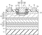
Next, the first embodiment of the present disclosure is described.Be shown in Fig. 1 according to the schematic formation of the semiconductor device of the first embodiment.Semiconductor device shown in Fig. 1 is so-called MISJPHEMT, it is included in the barrier layer between grid and channel layer, in barrier layer, be also provided with the low resistance region that conductivity type is different from the conductivity type on barrier layer, in addition, grid is arranged on low resistance region via dielectric film.
In the semiconductor device shown in Fig. 1, resilient coating 12, lower barrier 13, channel layer 14, upper barrier 15 and the clearance layer 22 be made up of each compound semiconductor materials are deposited in order on the substrate 11 of being made up of compound semiconductor with this.
In lower barrier 13, be provided with charge carrier supplying layer 13a.In upper barrier 15, be provided with p-type low resistance region 15d and charge carrier supplying layer 15a.
Then,, on the duplexer of the above-mentioned semiconductor layer of being made by compound semiconductor materials, insulating barrier 17 is set.On insulating barrier 17, opening 17a and 17b are set.In opening 17a and 17b, form source electrode 18 and drain electrode 19, they are connected to upper barrier 15 via clearance layer 22.
In addition,, between opening 17a and 17b, opening 17c is arranged in insulating barrier 17 and clearance layer 22.Opening 17c is formed as making the A/F of clearance layer 22 to be greater than the A/F of insulating barrier 17.In opening 17c, in upper barrier 15, form gate insulating film 16 along bottom surface and the side of opening 17c.
Lower barrier
Channel layer
For example, in the situation that channel layer 14 is formed by InGaAs mixed crystal, preferably, in III element, indium ratio of components is equal to or higher than 0.1.Indium ratio of components is higher, and band gap can be narrower.If indium ratio of components is equal to or higher than 0.1, can make so the difference of the each conduction band position between lower barrier 13 and channel layer 14 and between upper barrier 15 and channel layer 14 enough large.In addition, preferably, the thickness of channel layer 14 is equal to or less than 15nm.This be because in the time that channel layer 14 becomes thicker its crystallinity deterioration.
Upper barrier
In the situation that upper barrier 15 is formed by AlGaAs mixed crystal, preferably, in iii group element, aluminium ratio of components is equal to or less than 0.25.By making aluminium ratio of components be equal to or less than 0.25, can suppress the increase of so-called source resistance.In addition, described later by p-type impurity diffuse to form p-type low resistance region 15d time, can suppress diffusion velocity, and can improve controllability.
P-type low resistance region 15d is the diffusion zone of highdensity p-type impurity.P-type low resistance region 15d is the p-type low resistance region arranging corresponding to grid 20 in the region between source electrode 18 and drain electrode 19.P-type low resistance region 15d is between gate insulating film 16 and resistive formation 15b, and for example by forming as p-type impurity and the zinc (Zn) that is diffused in a part of resistive formation 15b.Preferably, in p-type low resistance region 15d, the density of p-type impurity is equal to or higher than 1 × 10
18cm
-3.
For example, upper barrier 15 comprises that thickness is 4nm and adds as approximately 3 × 10 of N-shaped impurity
18cm
-3the charge carrier supplying layer 15a of silicon.Then, upper barrier 15 has following structure: be wherein that 2nm and the resistive formation 15c that does not add impurity and thickness are that 30nm and the resistive formation 15b that does not add impurity are from channel layer 14 sides depositions at the upper and lower thickness of charge carrier supplying layer 15a.
In addition, to have wherein p-type impurity density be approximately 1 × 10 to upper barrier 15
19cm
-3p-type low resistance region 15d in contacting with gate insulating film 16, be embedded in the structure in resistive formation 15b.
In addition, in this example, illustrated that wherein lower barrier 13 and upper barrier 15 are by the Al of same composition
0.2ga
0.8the example that As mixed crystal forms.But lower barrier 13 and upper barrier 15 can form by having the AlGaAs mixed crystal forming that differs from one another.
In upper barrier 15, preferably, in iii group element, aluminium ratio of components is equal to or less than 0.25.On the contrary, in lower barrier 13, must be by p-type impurity diffuse to form p-type low resistance region.For this region, in the structure of lower barrier 13, aluminium ratio of components can be than upper barrier 15 height.
In addition, preferably, in resistive formation 13b and 15b, the density of impurity is equal to or less than 1 × 10
17cm
-3, and preferably, be equal to or higher than 1 × 10 than resistance
-2Ω cm.
Clearance layer
Insulating barrier
Insulating barrier 17 has insulating properties with respect to the compound semiconductor that forms upper barrier 15; and use and there is layer that protective ratio ionic impurity etc. is low (here; upper barrier 15) the material of function of surface, the silicon nitride (Si that insulating barrier 17 is for example 200nm by thickness
3n
4) form.
Gate insulating film
Grid
Current barrier region
In addition, as shown in Figure 1, current barrier region 21 is formed on the both sides of p-type low resistance region 15d.Having in the semiconductor device forming shown in Fig. 1, because fermi level pinning (Fermi level pinning) occurs the interfacial state between gate insulating film 16 and resistive formation 15b., because the interfacial state between gate insulating film 16 and the resistive formation 15b of upper barrier 15 produces depletion layer in resistive formation 15b.In this way, realize depletion layer in the both sides of grid 20 in the mode of current barrier region 21 and expand to the effect in semiconductor.
Use can be with shown in Fig. 2 A and Fig. 2 B to form explanation and how to form current barrier region 21 by interfacial state.Fig. 2 A is illustrated in gate insulating film 16 and upper barrier 15 and can be with formation in the situation that interface state density is low.In addition, Fig. 2 B is illustrated in gate insulating film 16 and upper barrier 15 and can be with formation in the situation that interface state density is high.
As shown in Figure 2 A, in the situation that interface state density is low, by voltage is applied on grid, at upper barrier 15 side accumulation electronics.For this reason, generation current path in the interface between gate insulating film 16 and upper barrier 15.On the contrary, as shown in Figure 2 B, in the situation that interface state density is high, be difficult to by voltage being applied on grid and at upper barrier 15 side accumulation electronics.For this reason, generation current path not in the interface between gate insulating film 16 and upper barrier 15.
Usually, compare with resistive formation 15b with p-type low resistance region 15d, highdensity interfacial state is easily formed on the deep-seated of band gap and puts in resistive formation 15b and gate insulating film 16.For this reason, the depletion layer that plays contribution as the current barrier region in resistive formation 15b is easily extended from the interface of gate insulating film 16 and resistive formation 15b.
In addition,, because grid 20 does not contact with this region, be therefore not easy to be subject to being applied to the impact of the voltage on grid.Therefore, even if apply positive voltage, the width of depletion layer is also not easy to change, thereby in the wide region that is applied to the voltage on grid, anticipates the effect of current barrier region.
MISJPHEMT: operation
Can band
In Fig. 3 and Fig. 4, be illustrated in and can be with formation under the grid 20 of semiconductor device of above-mentioned formation.Fig. 3 illustrates the state of the gate voltage Vg that applies about zero volt.Fig. 4 illustrates the state of the gate voltage Vg that applies approximately 3 volts.In addition, in Fig. 3 and Fig. 4, show semiconductor device, wherein lower barrier 13 and upper barrier 15 are by Al
0.2ga
0.8as mixed crystal forms, and channel layer 14 is by In
0.2ga
0.8as mixed crystal forms.
As shown in Figure 3, above-mentioned semiconductor device is constructed such that enough large (0.31eV) of discontinuous quantity Δ Ec of the conduction band edge of channel layer 14 and upper barrier 15 here.In addition, semiconductor device is constructed such that enough large (, more than the 0.20eV) of difference between the Fermi level of the electronics in current potential smallest point and the channel layer 14 of upper barrier 15 here.For this reason, little of negligible degree compared with electron amount in channel layer 14 interior distributions at the electron amount of upper barrier 15 interior distributions.
In addition, above-mentioned semiconductor device has wherein channel layer 14 and is clipped in conduction band position than the formation between channel layer 14 high lower barrier 13 and upper barrier 15.For this reason, in the time of the charge carrier supplying layer 13a from lower barrier 13 and upper barrier 15 and 15a supply charge carrier, channel layer 14 accumulation charge carriers, and become Two-dimensional electron gas-bearing formation.
In this semiconductor device, gate insulating film is arranged between grid and the first conductivity type p-type low resistance region, do not exist resemble in the situation of pn knot the large mobile situation of forward current.For this reason, grid leakage current can greatly reduce, and large positive voltage can be applied on grid 20.
In addition, as shown in Figure 1, semiconductor device has current barrier region 21 in the both sides of p-type low resistance region 15d.In this way, by positive voltage being applied on grid 20, even carry out producing charge carrier in reverse turn operation and the interface between gate insulating film 16 and p-type low resistance region 15d in the MIS structure being formed by grid 20, gate insulating film 16 and p-type low resistance region 15d, these charge carriers can not contribute to electric current to flow between source electrode 18 and drain electrode 19.
Operation
In the semiconductor device of above-mentioned formation, be applied under the state on grid 20 at the gate voltage Vg of about zero volt, the valence band location Ev in the p-type low resistance region 15d under gate insulating film 16 is constant, and substantially mates with Fermi level Ef.
In addition, at gate voltage Vg lower than threshold voltage in the situation that, as shown in Figure 5, in semiconductor device, the carrier depletion region 14a of depleted of electrons is formed on the region that is arranged in the channel layer 14 under p-type low resistance region 15d.The formation of being with is now shown in Fig. 3.In this way, because carrier depletion region 14a makes channel layer 14 in high resistance state.Therefore,, between source electrode 18 and drain electrode 19, drain current Id can not flow via channel layer 14, and semiconductor device becomes OFF state.
On the other hand, be applied under the state on the grid 20 of semiconductor device at the positive gate voltage Vg of approximately 3 volts, the conduction band position Ec of p-type low resistance region 15d reduces via gate insulating film 16.For this reason, 15dNei hole, p-type low resistance region exhausts.The formation of being with is now shown in Fig. 4.
In addition, now, the carrier depletion region 14a in the channel layer 14 shown in Fig. 5 disappears.For this reason, electron amount in channel layer 14 increases, and drain current Id between source electrode 18 and drain electrode 19 flows via channel layer 14.Drain current Id is modulated by gate voltage Vg.
In the JPHEMT of prior art, the voltage being applied on grid is equal to or less than 1.0V.But the voltage being applied in this semiconductor device on grid must not be equal to or less than 1.0V.,, compared with JPHEMT, in illustrative semiconductor device, high positive voltage can be applied on grid 20.For this reason, the ON resistance R on of channel layer 14 reduces, and maximum drain current Idmax increases.In addition, the size of element can reduce, and parasitic capacitance can reduce.
Current barrier region
By the way, in the semiconductor device of above-mentioned formation, in the case of not comprising the formation of current barrier region, in the time being equal to or higher than the positive gate voltage Vg of 3.0V and being applied on grid 20, there is following phenomenon.
In the time that positive gate voltage Vg is applied on grid 20, the conduction band position of p-type low resistance region 15d reduces via gate insulating film 16, and starts to occur reverse turn operation in the region of gate insulating film 16 and p-type low resistance region 15d.For this reason, the electron amount existing in the interface between dielectric film and semiconductor increases, and forms the path that the drain current Id beyond channel layer 14 flows through.Now, because drain current Id is the summation that flows through the electric current of reverse turn operation portion and channel layer 14, therefore the total value of drain current becomes large.The formation of being with is now shown in Fig. 6.
In Fig. 7, the electric current distribution on grid side in the time applying gate voltage is shown.Due to by the difference that has or not to evaluate electric current of current barrier region, therefore the current density in the VII-VII line sectional view in Fig. 1 is shown in Fig. 7.Here the situation that has a current barrier region, is the situation of the semiconductor device that forms shown in above-mentioned Fig. 1.In addition the situation that, does not have a current barrier region is the situation of having removed current barrier region 21 semiconductor device from forming shown in above-mentioned Fig. 1.
As shown in Figure 7, not having in the semiconductor device of current barrier region, generation current in the interface (interface between gate insulating film and semiconductor) in channel layer 14 and between gate insulating film 16 and resistive formation 15b.
On the contrary, in the semiconductor device with current barrier region, only generation current in channel layer 14, generation current not in the interface between gate insulating film 16 and resistive formation 15b.In this way, mobile electric current in the interface can be suppressed at reverse turn operation by current barrier region 21 time between dielectric film and semiconductor.
In the inversion layer forming in interface between insulating barrier and semiconductor, the mobility of the electronics of traveling is different from the mobility of the electronics of traveling in channel layer 14.In the semi-conducting material using in the upper barrier 15 being represented by AlGaAs layer, the mobility of the electronics of traveling is 1000~3000cm
2/ V-sec, than low in channel layer 14.Therefore, as the Transfer conductance (gm of one of transistorized operational capacity; With respect to the variation that is applied to the voltage on grid, the variable quantity of drain current) show the very large interdependence to being applied to the voltage on grid, because the place of electronics traveling is increased to 2 places from 1 place.This state is shown in Fig. 8.
As shown in Figure 8, not having in the semiconductor device of current barrier region, in the time that the voltage applying is equal to or higher than 3 volts, can find out the rising of Transfer conductance.On the other hand, having in the semiconductor device of current barrier region 21, even be equal to or higher than 3 volts at the voltage applying, Transfer conductance does not also rise.In this way, by comprising current barrier region 21, be appreciated that the gate voltage interdependence of Transfer conductance gm is very little.For example, in the situation that supposition is applied to duplexer, the gate voltage interdependence of Transfer conductance gm affects the distorted characteristic of switch.Therefore, having in the MISJPHEMT of current barrier region 21, distorted characteristic deteriorated very little.
Advantage
According to the semiconductor device of disclosure embodiment, because gate insulating film 16 is formed between grid 20 and p-type low resistance region 15d (interface between gate insulating film and semiconductor), therefore grid leakage current flows hardly in this interface.For this reason, high positive voltage can be applied on grid 20, and can reduce ON resistance R on.In addition, can increase maximum drain current Idmax.
In addition, this semiconductor device has current barrier region, even and because the voltage being applied on grid increases, the gate voltage interdependence of Transfer conductance gm is also very low, therefore, compared with the formation that does not there is current barrier region with semiconductor device wherein, the harmonic distortion characteristic can be suppressed at ON time deteriorated.
Therefore, if use this semiconductor device structure wireless communication apparatus, the size of wireless communication apparatus can reduce, and power consumption can reduce.That is to say, especially, in communication terminal, the size of device can miniaturization, and the operating time can extend, and can also make it be easier to carry.
In addition,, because gate insulating film 16 is formed between grid 20 and p-type low resistance region 15d, therefore can improve the proof voltage between grid 20 and drain electrode 19.
3. the first embodiment (manufacturing the method for semiconductor device)
Next, the method for the semiconductor device of manufacturing above-mentioned the first embodiment is described.
First, as shown in Figure 9 A, depositing semiconductor layers on substrate 11.
For example, on the substrate 11 of being made up of GaAs, the u-GaAS layer that does not for example add impurity by epitaxial growth forms resilient coating 12.Then, on resilient coating 12, for example, by epitaxial growth AlGaAs (Al
0.2ga
0.8as mixed crystal) layer formation lower barrier 13.Now, the resistive formation 13c that order epitaxial growth is made up of the u-AlGaAs layer that does not add impurity, the charge carrier supplying layer 13a being made by the N-shaped AlGaAs layer that adds silicon (Si) and the resistive formation 13b being made by the u-AlGaAs layer that does not add impurity.In this way, form lower barrier 13, it is included in the central N-shaped charge carrier supplying layer 13a of film thickness direction.
Next,, in lower barrier 13, the u-InGaAs layer that does not add impurity by epitaxial growth forms channel layer 14.
Then, on channel layer 14, by epitaxial growth AlGaAs (Al
0.2ga
0.8as mixed crystal) layer formation upper barrier 15, now, the resistive formation 15c that order epitaxial growth is made up of the u-AlGaAs layer that does not add impurity, the charge carrier supplying layer 15a being made by the N-shaped AlGaAs layer that adds silicon (Si) and the resistive formation 15b being made by the u-AlGaAs layer that does not add impurity.In this way, obtain upper barrier 15, it is included in the central N-shaped charge carrier supplying layer 15a of film thickness direction.
In addition,, in upper barrier 15, for example, interpolation is formed clearance layer 22 as the N-shaped GaAs layer of the silicon of N-shaped impurity.
Then, inject (not shown) by mesa etch or isolation and carry out interelement separation.
Next, as shown in Figure 9 B, in clearance layer 22, by using chemical vapour deposition (CVD) (PECVD) the method formation silicon nitride film that for example plasma strengthens to form insulating barrier 17.Then,, by carry out pattern etching on insulating barrier 17, on grid formation region, form the surperficial opening 17c that exposes upper barrier 15.In this state, introduce p-type impurity by the surface from the clearance layer 22 exposed in the bottom of opening 17c, in upper barrier 15, form p-type low resistance region 15d.For example,, by form p-type low resistance region 15d in clearance layer 22 and resistive formation 15b using being diffused into as the zinc of p-type impurity at the temperature of approximately 600 ℃.Here, by forming p-type low resistance region 15d using be diffused into the position that do not arrive charge carrier supplying layer 15a (, only the superficial layer in resistive formation 15b on) as the zinc (Zn) of p-type impurity.The diffusion of zinc (Zn) for example utilizes the zinc compound gas at the temperature of approximately 600 ℃ to be undertaken by gas phase diffusion.In this way, form p-type low resistance region 15d by the autoregistration on the bottom at opening 17c.
Next, forming after p-type low resistance region 15d, for example, using citric acid is that etching solution is optionally only removed the part that clearance layer 22 is exposed from opening 17c.Then,, on the resistive formation 15b of upper barrier 15 that removes insulating barrier 17 and on insulating barrier 17, by using ald (ALD) method deposition of aluminum oxidation film, form gate insulating film 16.
Forming after gate insulating film 16, by nickel deposited and gold form pattern and form grid 20 successively on gate insulating film 16.
Next, by etching selectivity remove gate insulating film 16 and insulating barrier 17, the source electrode that then clamps betwixt p-type low resistance region 15d forms region and drain electrode and forms in region and form respectively opening 17a and opening 17b.Then, for example, AuGe, nickel and gold are sequentially deposited in opening 17a and opening 17b, and form pattern.Subsequently, by the heat treatment at about 400 ℃, be associated gold and form respectively source electrode 18 and drain electrode 19 by forming gold, can form like this semiconductor device shown in Fig. 1.
In the gap on grid side, due to the interfacial state between gate insulating film 16 and the resistive formation 15b of upper barrier 15, depletion layer expands to resistive formation 15b, and to as 21 contributions of current barrier region.Usually, relatively p-type low resistance region 15d and resistive formation 15b, puts at the deep-seated of the band gap of the latter and gate insulating film 16, easily forms highdensity interfacial state.For this reason, to easily expanding as the depletion layer of 21 contributions of current barrier region.In addition, grid 20 does not contact with this region, is not easy to be subject to being applied to the impact of the voltage on grid.Therefore, even in the time applying positive voltage, depletion layer is also not easy to change, and in the wide region of gate voltage, anticipates the effect of current barrier region.
This semiconductor device is for example preferred for the wireless communication apparatus in wireless telecommunication system.As wireless communication apparatus, communication frequency is that hyperfrequency (UHF) device more than frequency band is preferred.
According to the semiconductor device of the present embodiment, because gate insulating film 16 is formed between grid 20 and p-type low resistance region 15d, therefore grid leakage current flows in the interface between gate insulating film 16 and resistive formation 15b hardly.For this reason, large positive voltage can be applied on grid 20, and can reduce ON resistance R on.In addition, can increase maximum drain current Idmax.
If use this semiconductor device structure wireless communication apparatus, the size of wireless communication apparatus can reduce, and power consumption can reduce.That is to say, especially, in communication terminal, the size of device can miniaturization, and the operating time can extend, and can also make it be easier to carry.
In addition,, because gate insulating film 16 is formed between grid 20 and p-type low resistance region 15d, therefore can improve the proof voltage between grid 20 and drain electrode 19.
In addition,, according to the manufacture method of the semiconductor device in the present embodiment, the resistive formation 15b being formed by the band gap semiconductor wider than the semiconductor that forms channel layer 14 is formed between channel layer 14 and gate insulating film 16.Then,, on resistive formation 15b, form p-type low resistance region 15d by diffusion corresponding to the p-type impurity of grid 20.Therefore, can easily manufacture the semiconductor device in the present embodiment.
4. the second embodiment (semiconductor device)
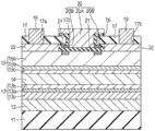
Next, the second embodiment of semiconductor device is described.The second embodiment and above-mentioned the first embodiment are similar.The semiconductor device of the second embodiment is so-called MISJPHEMT, and wherein barrier layer is arranged between grid and channel layer, and the low resistance region of the conductivity type different from barrier layer is arranged in barrier layer.In addition,, in the second embodiment, the formation identical with above-mentioned the first embodiment represents with identical Reference numeral, and no longer repeats to describe in detail.
The formation of the semiconductor device of the second embodiment is shown in Figure 10.As shown in figure 10, in semiconductor device, the resilient coating 12, lower barrier 13, channel layer 14, upper barrier 15 and the clearance layer 22 that are formed by compound semiconductor materials are deposited in order on substrate 11 with this.
In lower barrier 13, be provided with charge carrier supplying layer 13a.In upper barrier 15, be provided with p-type low resistance region 15d and charge carrier supplying layer 15a.
In addition,, on the duplexer of each layer of making at above-mentioned compound semiconductor materials, be provided with insulating barrier 17.On insulating barrier 17, be provided with opening 17a and 17b.In opening 17a and 17b, form the source electrode 18 and the drain electrode 19 that are connected with upper barrier 15 via clearance layer 22.
Between opening 17a and 17b, in insulating barrier 17 and clearance layer 22, be provided with opening 17c.In the clearance layer 22 of opening 17c under insulating barrier 17 and insulating barrier 17, form continuously, and be formed as making the A/F of clearance layer 22 larger than the A/F of insulating barrier 17.
The formation of above-mentioned formation and above-mentioned the first embodiment is similar.
In opening 17c, in upper barrier 15, form gate insulating film 16 along bottom surface and the side of opening 17c.In opening 17c, the gate insulating film 16 in sidewall and the upper barrier 15 of clearance layer 22 is formed as the thin thickness half of Thickness Ratio clearance layer 22.For this reason, the gap 23 being surrounded by the side of gate insulating film 16 and grid 20 is arranged on the identical layer of clearance layer 22.
For this reason, shown in formation in, gap 23 is arranged on the side of grid 20.Because gap 23 is arranged between grid 20 and current barrier region 21, therefore, compared with the situation of the first embodiment, can further suppress to be applied to the voltage impact on current barrier region via gate insulating film on grid.
5. the 3rd embodiment (semiconductor device)
Next, the 3rd embodiment of semiconductor device is described.The 3rd embodiment and above-mentioned the first embodiment are similar.The semiconductor device of the 3rd embodiment is so-called MISJPHEMT, and wherein barrier layer is arranged between grid and channel layer, and the low resistance region of the conductivity type different from barrier layer is arranged in barrier layer.In addition,, in the 3rd embodiment, the formation identical with above-mentioned the first embodiment represents with identical Reference numeral, and no longer repeats to describe in detail.
The formation of the semiconductor device of the 3rd embodiment is shown in Figure 11.As shown in figure 11, in semiconductor device, the resilient coating 12, lower barrier 13, channel layer 14, upper barrier 15 and the clearance layer 22 that are formed by compound semiconductor materials are deposited in order on substrate 11 with this.
In lower barrier 13, be provided with charge carrier supplying layer 13a.In upper barrier 15, be provided with p-type low resistance region 15d and charge carrier supplying layer 15a.
On the duplexer of each layer of making at above-mentioned compound semiconductor materials, be provided with insulating barrier 17.On insulating barrier 17, be provided with opening 17a and 17b.In opening 17a and 17b, form the source electrode 18 and the drain electrode 19 that are connected with upper barrier 15 via clearance layer 22.
The formation of above-mentioned formation and above-mentioned the first embodiment is similar.
In addition,, between opening 17a and 17b, in insulating barrier 17 and clearance layer 22, be provided with opening 17c and 17d.Opening 17c is arranged at the position that forms grid 20 in insulating barrier 17 and clearance layer 22.Opening 17d is arranged on the both sides of opening 17c within a predetermined distance.In the bottom of insulating barrier 17, the opening of clearance layer 22 is configured such that opening 17c and opening 17d are connected to the layer identical with clearance layer 22.Then, gate insulating film 16 forms continuously to upper barrier 15 from opening 17d in the opening of clearance layer 22.In addition, grid 20 is formed on the top of gate insulating film 16 from opening 17c.P-type low resistance region 15d via gate insulating film 16 be formed on grid 20 under.
In addition,, in resistive formation 15b, current barrier region 21 is arranged on the gate insulating film 16 times of opening 17d below.
In the time forming p-type low resistance region 15d or in process after a while, by impurity is incorporated into resistive formation 15b from opening 17d, form current barrier region 21.For example, by making insulating barrier 17 openings, on the both sides of opening 17c and opening 17c, opening 17d is set.Then, by introducing impurity from opening 17c and 17d, under opening 17c, form p-type low resistance region 15d, under opening 17d, form current barrier region 21.This region is made up of pn knot, and depletion layer extends to resistive formation 15b side, and to as 21 contributions of current barrier region.Because grid 20 does not apply voltage directly over current barrier region 21 and via thick dielectric film, therefore in the time applying gate voltage, the variation of the depletion layer of current barrier region 21 is very little.For this reason, though due to reverse turn operation in the situation that there is electronics between p-type low resistance region 15d and gate insulating film 16, depletion layer also can be to playing contribution as current barrier region.
6. the 4th embodiment (semiconductor device)
Next, the 4th embodiment of semiconductor device is described.The 4th embodiment and above-mentioned the first embodiment are similar.The semiconductor device of the 4th embodiment is so-called MISJPHEMT, and wherein barrier layer is arranged between grid and channel layer, and the low resistance region of the conductivity type different from barrier layer is arranged in barrier layer.In addition,, in the 4th embodiment, the formation identical with above-mentioned the first embodiment represents with identical Reference numeral, and no longer repeats to describe in detail.
The formation of the semiconductor device of the 4th embodiment is shown in Figure 12.As shown in figure 12, in semiconductor device, the resilient coating 12, lower barrier 13, channel layer 14, upper barrier 15 and the clearance layer 22 that are formed by compound semiconductor materials are deposited in order on substrate 11 with this.
In lower barrier 13, be provided with charge carrier supplying layer 13a.In upper barrier 15, be provided with p-type low resistance region 15d and charge carrier supplying layer 15a.
In addition,, on the duplexer of each layer of making at above-mentioned compound semiconductor materials, be provided with insulating barrier 17.On insulating barrier 17, be provided with opening 17a and 17b.In opening 17a and 17b, form the source electrode 18 and the drain electrode 19 that are connected with upper barrier 15 via clearance layer 22.
Between opening 17a and 17b, in insulating barrier 17 and clearance layer 22, be provided with opening 17c.In the clearance layer 22 of opening 17c under insulating barrier 17 and insulating barrier 17, form continuously, and be formed as making the A/F of clearance layer 22 larger than the A/F of insulating barrier 17.
The formation of above-mentioned formation and above-mentioned the first embodiment is similar.
In opening 17c, in upper barrier 15, form gate insulating film 16 along bottom surface and the side of opening 17c.Gate insulating film 16 forms by first grid dielectric film 16A with by the second gate dielectric film 16B making with first grid dielectric film 16A different materials.
On gate insulating film 16, form grid 20.P-type low resistance region 15d via first grid dielectric film 16A be formed on grid 20 under.In addition, current barrier region 21 is formed on the surface of upper barrier 15 and below the gate insulating film 16 of 15d both sides, p-type low resistance region.Current barrier region 21 is arranged on the position that contacts with second gate dielectric film 16B and on the surface of upper barrier 15.
First grid dielectric film 16A is only arranged on the below of grid 20.In addition, on the side of the opening 17c of second gate dielectric film 16B beyond being arranged under grid 20.That is, in the semiconductor device of this example, two gate insulating films 16 being made by mutual different materials be respectively formed at grid 20 under and on the side of opening 17c.
Compared with the interfacial state forming between first grid dielectric film 16A and p-type low resistance region 15d, the interfacial state forming in the interface between second gate dielectric film 16B and resistive formation 15b is set the dark state in semiconductor for, and makes density higher.For this reason, in the interfacial state forming between second gate dielectric film 16B and resistive formation 15b, very little to the variation of the depletion layer causing on grid owing to applying voltage.Therefore, though due to reverse turn operation in the situation that there is electronics between p-type low resistance region 15d and second gate dielectric film 16B, depletion layer also can be to as 21 contributions of current barrier region.
The example with the dielectric film of second gate dielectric film 16B function comprises for example SiN and SiO
2.On the other hand, as the first grid dielectric film 16A under grid 20, for example, can use Al
2o
3and HfO
2.
In addition,, for second gate dielectric film 16B, by changing the amount of negative fixed charge and the amount of interface dipole, can form current barrier region 21.Figure 13 A and Figure 13 B illustrate and can be with due to what the difference of the fixed charge amount of the material using in gate insulating film 16 caused the variation forming.Figure 13 A is illustrated in the situation that gate insulating film 16 do not have negative fixed charge and can be with the figure forming under grid 20.In addition, Figure 13 B is illustrated in the situation that gate insulating film 16 has negative fixed charge and can be with the figure forming under grid 20.
As shown in Figure 13 B, by changing the amount of fixed charge and the amount of interface dipole, the voltage that can form the accumulation layer in MIS interface can move.For this reason, electronics is not easy to pass through-Qf/Cox accumulation, and second gate dielectric film 16B can be to as 21 contributions of current barrier region.In this way, by changing the negative fixed charge amount of second gate dielectric film 16B and the amount of interface dipole, can on the interface, top of second gate dielectric film 16B and upper barrier 15, form current barrier region 21.As the dielectric film of introducing fixed charge, for example, report that wherein H is introduced into Al
2o
3in material.
7. the 5th embodiment (semiconductor device)
Next, the 5th embodiment of semiconductor device is described.The 5th embodiment and above-mentioned the first embodiment are similar.The semiconductor device of the 5th embodiment is so-called MISJPHEMT, and wherein barrier layer is arranged between grid and channel layer, and the low resistance region of the conductivity type different from barrier layer is arranged in barrier layer.In addition,, in the 5th embodiment, the formation identical with above-mentioned the first embodiment represents with identical Reference numeral, and no longer repeats to describe in detail.
The formation of the semiconductor device of the 5th embodiment is shown in Figure 14.As shown in figure 14, in semiconductor device, the resilient coating 12, lower barrier 13, channel layer 14, upper barrier 15 and the clearance layer 22 that are formed by compound semiconductor materials are deposited in order on substrate 11 with this.
In lower barrier 13, be provided with charge carrier supplying layer 13a.In upper barrier 15, be provided with p-type low resistance region 15d and charge carrier supplying layer 15a.
In addition,, on the duplexer of each layer of making at above-mentioned compound semiconductor materials, be provided with insulating barrier 17.On insulating barrier 17, be provided with opening 17a and 17b.In opening 17a and 17b, form the source electrode 18 and the drain electrode 19 that are connected with upper barrier 15 via clearance layer 22.
Between opening 17a and 17b, in insulating barrier 17 and clearance layer 22, be provided with opening 17c.In the clearance layer 22 of opening 17c under insulating barrier 17 and insulating barrier 17, form continuously, and it is large to be formed as the opening of the aperture efficiency insulating barrier 17 that makes clearance layer 22.
The formation of above-mentioned formation and above-mentioned the first embodiment is similar.
In addition,, in opening 17c, in upper barrier 15, form gate insulating film 16 along bottom surface and the side of opening 17c.In opening 17c, the gate insulating film 16 in sidewall and the upper barrier 15 of clearance layer 22 is formed as thin in Thickness Ratio the first embodiment.Similar in the formation of gate insulating film 16 and above-mentioned the second embodiment.
In this example, on gate insulating film 16, form grid 20.In addition,, in the wider scope of the opening than being located at the opening 17c in insulating barrier 17, on the gate insulating film 16 of being located at the opening 17c in clearance layer 22, form grid 20.
In addition, p-type low resistance region 15d via gate insulating film 16 be formed on first grid 20A under.In addition, current barrier region 21 be formed on the surface of upper barrier 15 and via the gate insulating film 16 of 15d both sides, p-type low resistance region under second grid 20B.
In semiconductor device, the metal that work function is larger than first grid 20A is used for second grid 20B.Figure 15 A and Figure 15 B illustrate the variation that can be with formation causing according to the work function difference of the metal using in grid 20.Figure 15 A and Figure 15 B are illustrated in has little work function (W
m1) material be applicable in the situation of grid 20 and there is large work function (W
m2) material be applicable in the situation of grid 20 can be with formation in grid 20.
As shown in Figure 15 A and Figure 15 B, there is the metal of large work function by use, from formula Δ V=W
m2-W
m1in known, electronics is not easy to be accumulated in the Δ V of interface, forms as the voltage of the accumulation layer of current path and moves to positive bias direction.Therefore, in the MIS structure being formed by second grid 20B, gate insulating film 16 and resistive formation 15b, due to cumulative operation be applied to voltage on grid with respect to the MIS structural transfer being formed by first grid 20A, gate insulating film 16 and p-type low resistance region 15d to positive direction.For this reason, even in the time that the latter's MIS structure is carried out reverse turn operation, the former MIS structure division also can maintain the function as current barrier region.In this way, there is the material of large work function by use as second grid 20B, can on the interface, top of upper barrier 15, form current barrier region 21.
As the example of the metal with large work function of function of realizing second grid 20B, can comprise Ni, Pd, Pt and Au etc.
8. the 6th embodiment (semiconductor device)
Next, the 6th embodiment of semiconductor device is described.
In above-mentioned each embodiment, having illustrated to introduce has the semiconductor device of the current barrier region based on MISJPHEMT structure and its manufacture method.But the contribution of current barrier region is not only effective for MISJPHEMT, and also effective for MISPHEMT.
Hereinafter, illustrate that current barrier region is wherein incorporated into the formation in the semiconductor device of MISPHEMT structure.In the semiconductor device of the MISPHEMT structure described in the 6th embodiment, the formation identical with the semiconductor device of the MISJPHEMT structure described in above-mentioned the first embodiment represents with identical Reference numeral, and no longer repeats to describe in detail.
MISPHEMT
The formation of the semiconductor device of the 6th embodiment is shown in Figure 16.As shown in figure 16, in semiconductor device, the resilient coating 12, lower barrier 13, channel layer 14, upper barrier 15 and the clearance layer 22 that are formed by compound semiconductor materials are deposited in order on substrate 11 with this.
In lower barrier 13, be provided with charge carrier supplying layer 13a.In upper barrier 15, be provided with charge carrier supplying layer 15a.
In addition, different from the MISJPHEMT structure described in the first embodiment, p-type low resistance region is not arranged in upper barrier 15.
Then,, on the duplexer of each layer of making at above-mentioned compound semiconductor materials, be provided with insulating barrier 17.On insulating barrier 17, be provided with opening 17a and 17b.In opening 17a and 17b, form the source electrode 18 and the drain electrode 19 that are connected with upper barrier 15 via clearance layer 22.
In addition,, between opening 17a and 17b, in insulating barrier 17 and clearance layer 22, be provided with opening 17c.In the clearance layer 22 of opening 17c under insulating barrier 17 and insulating barrier 17, form continuously.Opening 17c is formed as making the A/F of clearance layer 22 wider than the A/F of insulating barrier 17.
In opening 17c, in upper barrier 15, form gate insulating film 16 along bottom surface and the side of opening 17c.On the top of gate insulating film 16, form grid 20.In addition, current barrier region 21 is formed on below the gate insulating film 16 on the surface of upper barrier 15 and beyond under grid 20.
In the 6th embodiment, substrate 11, resilient coating 12, lower barrier 13, channel layer 14, gate insulating film 16, insulating barrier 17, source electrode 18, drain electrode 19, grid 20 and clearance layer 22 have and similarly form described in the first embodiment.In addition, upper barrier 15 has and similarly forms described in the first embodiment, except low resistance region is not set.
Current barrier region
As shown in figure 16, in the interface between gate insulating film 16 and resistive formation 15b, the both sides under the grid 20 of current barrier region 21 beyond being formed under grid 20.
Having in the semiconductor device forming shown in Figure 16, because fermi level pinning occurs the interfacial state between gate insulating film 16 and resistive formation 15b., because the interfacial state between gate insulating film 16 and the resistive formation 15b of upper barrier 15 produces depletion layer in resistive formation 15b.In this way, realize depletion layer in the both sides of grid 20 in the mode of current barrier region 21 and expand to the effect in semiconductor.
In the present example, use and can be with formation shown in Fig. 2 A and Fig. 2 B, can be by illustrating by interfacial state how to form current barrier region 21 with the similar mode of formation of the first embodiment.As shown in Figure 2 A, in the situation that interface state density is low, by voltage is applied on grid, at upper barrier 15 side accumulation electronics.For this reason, generation current path in the interface between gate insulating film 16 and upper barrier 15.On the contrary, as shown in Figure 2 B, in the situation that interface state density is high, even voltage is applied on grid, be also not easy at upper barrier 15 side accumulation electronics.For this reason, generation current path not in the interface between gate insulating film 16 and upper barrier 15.
Because current barrier region 21 is the regions that do not contact with grid 20, be therefore not easy to be subject to being applied to the impact of the voltage on grid.Therefore,, even if apply positive voltage, the width of depletion layer is also not easy to change.Therefore, in the wide region of gate voltage, anticipate the effect of current barrier region 21.
On the other hand, because the current barrier region 21 under grid 20 is to be subject to being applied to the region that the voltage on grid affects greatly, in the time applying positive voltage, the width of depletion layer easily changes, and is difficult to anticipate the effect of current barrier region.Therefore, this region is very little as the contribution of current barrier region.
In addition, the method for manufacturing the semiconductor device with the MISPHEMT structure described in the 6th embodiment is identical with the method for manufacturing the semiconductor device in above-mentioned the first embodiment, except not carrying out forming low resistance region by introducing impurity.
9. the 7th embodiment (semiconductor device)
Next, the 7th embodiment of semiconductor device is described.The semiconductor device of the 7th embodiment and above-mentioned the 6th embodiment are similar, are so-called MISPHEMT, comprising the barrier layer between grid and channel layer.In addition,, in the 7th embodiment, the formation identical with above-mentioned the 6th embodiment represents with identical Reference numeral, and no longer repeats to describe in detail.
The formation of the semiconductor device of the 7th embodiment is shown in Figure 17.As shown in figure 17, in semiconductor device, the resilient coating 12, lower barrier 13, channel layer 14, upper barrier 15 and the clearance layer 22 that are formed by compound semiconductor materials are deposited in order on substrate 11 with this.
In lower barrier 13, be provided with charge carrier supplying layer 13a.In upper barrier 15, be provided with charge carrier supplying layer 15a.
In addition,, on the duplexer of each layer of making at above-mentioned compound semiconductor materials, be provided with insulating barrier 17.On insulating barrier 17, be provided with opening 17a and 17b.In opening 17a and 17b, form the source electrode 18 and the drain electrode 19 that are connected with upper barrier 15 via clearance layer 22.
Between opening 17a and 17b, in insulating barrier 17 and clearance layer 22, be provided with opening 17c.In the clearance layer 22 of opening 17c under insulating barrier 17 and insulating barrier 17, form continuously.Opening 17c is formed as making the A/F of clearance layer 22 wider than the A/F of insulating barrier 17.
The formation of above-mentioned formation and above-mentioned the 6th embodiment is similar.
In opening 17c, in upper barrier 15, form gate insulating film 16 along bottom surface and the side of opening 17c.In opening 17c, the gate insulating film 16 in sidewall and the upper barrier 15 of clearance layer 22 is formed as the thin thickness half of Thickness Ratio clearance layer 22.For this reason, the gap 23 being surrounded by the side of gate insulating film 16 and grid 20 is arranged on the identical layer of clearance layer 22.
For this reason, shown in formation in, gap 23 is arranged on the side of grid 20.Because gap 23 is arranged between grid 20 and current barrier region 21, therefore, compared with the situation of the first embodiment, can further suppress to be applied to the voltage impact on current barrier region via gate insulating film on grid.
10. the 8th embodiment (semiconductor device)
Next, the 8th embodiment of semiconductor device is described.The 8th embodiment and above-mentioned the 6th embodiment are similar.The semiconductor device of the 8th embodiment is so-called MISPHEMT, comprising the barrier layer between grid and channel layer.In addition,, in the 8th embodiment, the formation identical with above-mentioned the 6th embodiment represents with identical Reference numeral, and no longer repeats to describe in detail.
The formation of the semiconductor device of the 8th embodiment is shown in Figure 18.As shown in figure 18, in semiconductor device, the resilient coating 12, lower barrier 13, channel layer 14, upper barrier 15 and the clearance layer 22 that are formed by compound semiconductor materials are deposited in order on substrate 11 with this.
In lower barrier 13, be provided with charge carrier supplying layer 13a.In upper barrier 15, be provided with charge carrier supplying layer 15a.
On the duplexer of each layer of making at above-mentioned compound semiconductor materials, be provided with insulating barrier 17.On insulating barrier 17, be provided with opening 17a and 17b.In opening 17a and 17b, form the source electrode 18 and the drain electrode 19 that are connected with upper barrier 15 via clearance layer 22.
The formation of above-mentioned formation and above-mentioned the 6th embodiment is similar.
In addition,, between opening 17a and 17b, in insulating barrier 17 and clearance layer 22, be provided with opening 17c and 17d.Opening 17c is arranged at the position that forms grid 20 in insulating barrier 17 and clearance layer 22.
In addition,, on the surface of resistive formation 15b, current barrier region 21 is arranged on the gate insulating film 16 times of opening 17d below.
By impurity is incorporated into resistive formation 15b from opening 17d, form current barrier region 21.For example, by making after insulating barrier 17 openings, form opening 17c, on the both sides of opening 17c, form opening 17d.Then,, by introducing impurity from opening 17c and 17d, under opening 17d, form current barrier region 21.This region is made up of pn knot, and the depletion layer that extends to resistive formation 15b side is to as 21 contributions of current barrier region.Because grid 20 does not apply voltage directly over current barrier region 21 and via thick dielectric film, therefore in the time applying voltage to grid, the variation of the depletion layer of current barrier region 21 is very little.For this reason, even in the time applying gate voltage, depletion layer also can be to playing contribution as current barrier region.
11. the 9th embodiments (semiconductor device)
Next, the 9th embodiment of semiconductor device is described.The semiconductor device of the 9th embodiment and above-mentioned the 6th embodiment are similar, are so-called MISPHEMT, comprising the barrier layer between grid and channel layer.In addition,, in the 9th embodiment, the formation identical with above-mentioned the 6th embodiment represents with identical Reference numeral, and no longer repeats to describe in detail.
The formation of the semiconductor device of the 9th embodiment is shown in Figure 19.As shown in figure 19, in semiconductor device, the resilient coating 12, lower barrier 13, channel layer 14, upper barrier 15 and the clearance layer 22 that are formed by compound semiconductor materials are deposited in order on substrate 11 with this.
In lower barrier 13, be provided with charge carrier supplying layer 13a.In upper barrier 15, be provided with charge carrier supplying layer 15a.
In addition,, on the duplexer of each layer of making at above-mentioned compound semiconductor materials, be provided with insulating barrier 17.On insulating barrier 17, be provided with opening 17a and 17b.In opening 17a and 17b, form the source electrode 18 and the drain electrode 19 that are connected with upper barrier 15 via clearance layer 22.
Between opening 17a and 17b, in insulating barrier 17 and clearance layer 22, be provided with opening 17c.In the clearance layer 22 of opening 17c under insulating barrier 17 and insulating barrier 17, form continuously.It is wide that opening 17c is formed as the A/F of the aperture efficiency insulating barrier 17 that makes clearance layer 22.
The formation of above-mentioned formation and above-mentioned the 6th embodiment is similar.
In opening 17c, in upper barrier 15, form gate insulating film 16 along bottom surface and the side of opening 17c.Gate insulating film 16 forms by first grid dielectric film 16A with by the second gate dielectric film 16B making with first grid dielectric film 16A different materials.
On gate insulating film 16, form grid 20.In addition, current barrier region 21 is formed on the both sides under the grid 20 on the surface of upper barrier 15 and beyond under grid 20.Current barrier region 21 is arranged on the position that contacts with second gate dielectric film 16B and on the surface of upper barrier 15.
First grid dielectric film 16A is only arranged on the below of grid 20.In addition, on the side of the opening 17c of second gate dielectric film 16B beyond being arranged under grid 20.That is, in the semiconductor device of this example, two gate insulating films 16 being made by mutual different materials be respectively formed at grid 20 under and on the side of opening 17c.
Compared with the interfacial state forming between first grid dielectric film 16A and resistive formation 15b, the interfacial state forming in the interface between second gate dielectric film 16B and resistive formation 15b is set the dark state in semiconductor for, and makes density higher.For this reason, in the interfacial state forming in the interface between second gate dielectric film 16B and resistive formation 15b, very little to the variation of the depletion layer causing on grid owing to applying voltage.Therefore, though due to reverse turn operation in the situation that there is electronics between resistive formation 15b and second gate dielectric film 16B, depletion layer also can be to as 21 contributions of current barrier region.
The example with the dielectric film of second gate dielectric film 16B function comprises for example SiN and SiO
2.On the other hand, as the first grid dielectric film 16A under grid 20, for example, can use Al
2o
3and HfO
2.
In addition,, for second gate dielectric film 16B, by changing the amount of negative fixed charge and the amount of interface dipole, can form current barrier region 21.Use and can be with formation shown in Figure 13 A and Figure 13 B, can be by with the similar mode of the 4th embodiment, the formation of the current barrier region 21 causing due to the difference of the fixed charge amount of the material of use in gate insulating film 16 being described.
As shown in Figure 13 B, by changing the amount of fixed charge and the amount of interface dipole, the voltage that can form the accumulation layer in MIS interface can move.For this reason, electronics is not easy to pass through-Qf/Cox accumulation, and MIS accumulation layer can be to as 21 contributions of current barrier region.In this way, by changing the negative fixed charge amount of second gate dielectric film 16B and the amount of interface dipole, can on the interface, top of upper barrier 15, form current barrier region 21.As the dielectric film of introducing fixed charge, for example, report that wherein H is introduced into Al
2o
3in material.
12. the tenth embodiments (semiconductor device)
Next, the tenth embodiment of semiconductor device is described.The tenth embodiment and above-mentioned the 6th embodiment are similar.The semiconductor device of the tenth embodiment is so-called MISPHEMT, and wherein barrier layer is arranged between grid and channel layer.In addition,, in the tenth embodiment, the formation identical with above-mentioned the 6th embodiment represents with identical Reference numeral, and no longer repeats to describe in detail.
The formation of the semiconductor device of the tenth embodiment is shown in Figure 20.As shown in figure 20, in semiconductor device, the resilient coating 12, lower barrier 13, channel layer 14, upper barrier 15 and the clearance layer 22 that are formed by compound semiconductor materials are deposited in order on substrate 11 with this.
In lower barrier 13, be provided with charge carrier supplying layer 13a.In upper barrier 15, be provided with charge carrier supplying layer 15a.
In addition,, on the duplexer of each layer of making at above-mentioned compound semiconductor materials, be provided with insulating barrier 17.On insulating barrier 17, be provided with opening 17a and 17b.In opening 17a and 17b, form the source electrode 18 and the drain electrode 19 that are connected with upper barrier 15 via clearance layer 22.
Between opening 17a and 17b, in insulating barrier 17 and clearance layer 22, be provided with opening 17c.In the clearance layer 22 of opening 17c under insulating barrier 17 and insulating barrier 17, form continuously, and be formed as making the A/F of clearance layer 22 wider than the A/F of insulating barrier 17.
The formation of above-mentioned formation and above-mentioned the 6th embodiment is similar.
In addition,, in opening 17c, in upper barrier 15, form gate insulating film 16 along bottom surface and the side of opening 17c.In opening 17c, the gate insulating film 16 in sidewall and the upper barrier 15 of clearance layer 22 is formed as thin in Thickness Ratio the 6th embodiment.Similar in the formation of gate insulating film 16 and above-mentioned the 7th embodiment.
In this example, on gate insulating film 16, form grid 20.In addition,, in the wider scope of the opening than being located at the opening 17c in insulating barrier 17, on the gate insulating film 16 of being located at the opening 17c in clearance layer 22, form grid 20.
In addition, current barrier region 21 is formed on the surface of upper barrier 15 and via gate insulating film 16 under second grid 20B.
In semiconductor device, the metal that work function is larger than first grid 20A is used for second grid 20B.Use and can be with formation shown in Figure 15 B, can be by with the similar mode of the 5th embodiment, the formation of the current barrier region 21 causing due to the work function difference of the metal of use in grid 20 being described.
As shown in Figure 15 A and Figure 15 B, there is the metal of large work function by use, from formula Δ V=W
m2-W
m1in known, electronics is not easy to be accumulated in the Δ V of interface, forms as the voltage of the accumulation layer of current path and moves to positive bias direction.Therefore, in the MIS structure being formed by second grid 20B, gate insulating film 16 and resistive formation 15b, due to cumulative operation be applied to voltage on grid with respect to the MIS structural transfer being formed by first grid 20A, gate insulating film 16 and resistive formation 15b to positive direction.For this reason, even in the time that the latter's MIS structure is carried out reverse turn operation, the former MIS structure division also can maintain the function as current barrier region 21.In this way, there is the material of large work function by use as second grid 20B, can on the interface, top of upper barrier 15, form current barrier region 21.
As the example of the metal with large work function of function of realizing second grid 20B, can comprise Ni, Pd, Pt and Au etc.
13. the 11 embodiments (semiconductor device)
Next, the 11 embodiment of semiconductor device is described.
In above-mentioned the 6th embodiment to the ten embodiments, illustrate and introduced the semiconductor device that has the current barrier region based on MISPHEMT structure.But the contribution of current barrier region is effective in the structure of the whole Surface Contact of gate insulating film and semiconductor surface.
Hereinafter, in the semiconductor device of MISPHEMT structure with current barrier region, the formation that gate insulating film contacts with semiconductor surface is described.In the semiconductor device of the MISPHEMT structure described in the 11 embodiment, the formation identical with the semiconductor device of the MISJPHEMT structure described in above-mentioned the 6th embodiment represents with identical Reference numeral, and no longer repeats to describe in detail.
MISPHEMT
The formation of the semiconductor device of the 11 embodiment is shown in Figure 21.As shown in figure 21, in semiconductor device, the resilient coating 12, lower barrier 13, channel layer 14, upper barrier 15 and the clearance layer 22 that are formed by compound semiconductor materials are deposited in order on substrate 11 with this.
In lower barrier 13, be provided with charge carrier supplying layer 13a.In upper barrier 15, be provided with charge carrier supplying layer 15a.
In addition, the opening 22c of formation grid 20 is arranged in clearance layer 22.
Then,, on the duplexer of each layer of making at above-mentioned compound semiconductor materials, gate insulating film 16 is configured to the top of coverage gap layer 22 and the top of the resistive formation 15b that exposes from the opening 22c of clearance layer 22.On gate insulating film 16, be provided with opening 17a and 17b.In opening 17a and 17b, form the source electrode 18 and the drain electrode 19 that are connected with upper barrier 15 via clearance layer 22.Opening 22c is arranged between opening 17a and opening 17b.In opening 22c, grid 20 is arranged on gate insulating film 16.In addition, current barrier region 21 is formed on below the gate insulating film 16 on the surface of upper barrier 15 and beyond under grid 20.
In the 11 embodiment, substrate 11, resilient coating 12, lower barrier 13, channel layer 14, source electrode 18, drain electrode 19, grid 20 and clearance layer 22 have and similarly form described in the first embodiment.In addition, upper barrier 15 has and similarly forms described in the 6th embodiment.Semiconductor device in this example has and similarly forms described in the 6th embodiment, and except insulating barrier is not arranged in clearance layer 22, but gate insulating film 16 is arranged in clearance layer 22 and grid 20 belows simultaneously.
Current barrier region
As shown in figure 21, in the interface between gate insulating film 16 and resistive formation 15b, the both sides under the grid 20 of current barrier region 21 beyond being formed under grid 20.
Having in the semiconductor device forming shown in Figure 21, because fermi level pinning occurs the interfacial state between gate insulating film 16 and resistive formation 15b., because the interfacial state between gate insulating film 16 and the resistive formation 15b of upper barrier 15 produces depletion layer in resistive formation 15b.In this way, realize depletion layer in the both sides of grid 20 in the mode of current barrier region 21 and expand to the effect in semiconductor.
In the present example, use and can be with formation shown in Fig. 2 A and Fig. 2 B, can be by illustrating by interfacial state how to form current barrier region 21 with the similar mode of formation of the first embodiment.As shown in Figure 2 A, in the situation that interface state density is low, by voltage is applied on grid, at upper barrier 15 side accumulation electronics.For this reason, generation current path in the interface between gate insulating film 16 and upper barrier 15.On the contrary, as shown in Figure 2 B, in the situation that interface state density is high, even voltage is applied on grid, be also not easy at upper barrier 15 side accumulation electronics.For this reason, generation current path not in the interface between gate insulating film 16 and upper barrier 15.
Because current barrier region 21 is the regions that do not contact with grid 20, be therefore not easy to be subject to being applied to the impact of the voltage on grid.Therefore,, even if apply positive voltage, the width of depletion layer is also not easy to change.Therefore, in the wide region that is applied to the voltage on grid, anticipate the effect of current barrier region 21.
On the other hand, because the current barrier region 21 under grid 20 is regions that the voltage that applied affects greatly, in the time applying positive voltage, the width of depletion layer easily changes, and is difficult to anticipate the effect of current barrier region.Therefore, this region is very little as the contribution of current barrier region.
14. the 12 embodiments (semiconductor device)
Next, the 12 embodiment of semiconductor device is described.The semiconductor device of the 12 embodiment becomes above-mentioned the 11 embodiment similar, is so-called MISPHEMT, has the wherein formation of the whole Surface Contact of gate insulating film and semiconductor surface.In addition,, in the 12 embodiment, the formation identical with above-mentioned the 11 embodiment represents with identical Reference numeral, and no longer repeats to describe in detail.
The formation of the semiconductor device of the 12 embodiment is shown in Figure 22.As shown in figure 22, in semiconductor device, the resilient coating 12, lower barrier 13, channel layer 14, upper barrier 15 and the clearance layer 22 that are formed by compound semiconductor materials are deposited in order on substrate 11 with this.
In lower barrier 13, be provided with charge carrier supplying layer 13a.In upper barrier 15, be provided with charge carrier supplying layer 15a.
In addition, the opening 17c of formation grid 20 is arranged in clearance layer 22.
Then, on the duplexer of each layer of making at above-mentioned compound semiconductor materials, dielectric film 24 is configured to the top of coverage gap layer 22 and the top of the resistive formation 15b that exposes from the opening 17c of clearance layer 22, and in the region of opening 17c beyond under grid 20.In addition, gate insulating film 16 is configured to cover the top of dielectric film 24 and the bottom surface of opening 17c.
On dielectric film 24 and gate insulating film 16, be provided with opening 17a and 17b.In opening 17a and 17b, form the source electrode 18 and the drain electrode 19 that are connected with upper barrier 15 via clearance layer 22.Opening 17c is arranged between opening 17a and opening 17b.In opening 17c, grid 20 is arranged on gate insulating film 16.In addition, current barrier region 21 is formed on the surface of upper barrier 15 and below dielectric film 24.
The example with the dielectric film of dielectric film 24 functions comprises for example SiN and SiO
2.On the other hand, as the gate insulating film 16 under grid 20, for example, can use Al
2o
3and HfO
2.
In addition,, for dielectric film 24, by changing the amount of negative fixed charge and the amount of interface dipole, can form current barrier region 21.Use and can be with formation shown in Figure 13 A and Figure 13 B, can be by with the similar mode of the 4th embodiment, the formation of the current barrier region 21 causing due to the difference of the fixed charge amount of the material of use in gate insulating film 16 being described.
As shown in Figure 13 B, by changing the amount of fixed charge and the amount of interface dipole, the voltage that can form the accumulation layer in MIS interface can move.For this reason, electronics is not easy to pass through-Qf/Cox accumulation, and MIS accumulation layer can be to as 21 contributions of current barrier region.In this way, by changing the negative fixed charge amount of dielectric film 24 and the amount of interface dipole, can on the interface, top of upper barrier 15, form current barrier region 21.As the dielectric film of introducing fixed charge, for example, report that wherein H is introduced into Al
2o
3in material.
As described in the present embodiment, by the insulating barrier in clearance layer and the integrated formation of gate insulating film, wherein the formation of the whole Surface Contact of gate insulating film and semiconductor surface goes for the semiconductor device described in the first to the tenth embodiment.
15. the 13 embodiments (semiconductor device)
Next, the 13 embodiment of semiconductor device is described.
In above-mentioned each embodiment, illustrate that the upper space of current barrier region is wherein formed on via the structure in the gate insulating film semiconductor layer relative with grid.But the upper space of current barrier region can be formed in the different semiconductor layer of the semiconductor layer relative from grid.
Hereinafter, in the semiconductor device of the MISJPHEMT of the first embodiment structure, illustrate that wherein the upper space of current barrier region is formed on the formation in the different semiconductor layer of the semiconductor layer relative from grid.In the semiconductor device of the MISJPHEMT structure of the 13 embodiment, the formation identical with the semiconductor device of the MISJPHEMT structure described in above-mentioned the first embodiment represents with identical Reference numeral, and no longer repeats to describe in detail.
The formation of the semiconductor device of the 13 embodiment is shown in Figure 23.As shown in figure 23, in semiconductor device, the resilient coating 12, lower barrier 13, channel layer 14, upper barrier 15, interlayer 25 and the clearance layer 22 that are formed by compound semiconductor materials are deposited in order on substrate 11 with this.
In lower barrier 13, be provided with charge carrier supplying layer 13a.In upper barrier 15, be provided with p-type low resistance region 15d and charge carrier supplying layer 15a.
In addition,, on the duplexer of each layer of making at above-mentioned compound semiconductor materials, be provided with insulating barrier 17.On insulating barrier 17, be provided with opening 17a and 17b.In opening 17a and 17b, form the source electrode 18 and the drain electrode 19 that are connected with upper barrier 15 via clearance layer 22 and interlayer 25.
In addition,, between opening 17a and 17b, opening 17c is arranged in insulating barrier 17, clearance layer 22 and interlayer 25.Opening 17c forms continuously in insulating barrier 17, clearance layer 22 and interlayer 25.Opening 17c is formed as making the A/F of clearance layer 22 wider than the A/F of insulating barrier 17, and the A/F of interlayer 25 is identical with the A/F of insulating barrier 17.
In opening 17c, in upper barrier 15, form gate insulating film 16 along bottom surface and the side of opening 17c.On the top of gate insulating film 16, form grid 20.P-type low resistance region 15d via gate insulating film 16 be formed on grid 20 under.In addition, current barrier region 21 is formed on the position on the surface of the interlayer 25 contacting with gate insulating film 16 and beyond under grid 20.Current barrier region 21 is formed in resistive formation 15b continuously from the surface of interlayer 25.
Use with the interface of gate insulating film 16 in the interface state density that the forms material formation interlayer 25 higher than the material that is applicable to resistive formation 15b.For example, Appl.Phys.Lett., 63, (1993) reported in p.379 InGaP based material with the interface of dielectric film in the interface state density that forms be less than GaAs based material.
Therefore, in the semiconductor device of this example, the resistive formation 15b of upper barrier 15 is formed by InGaP based material, and interlayer 25 is formed by AlGaAs based material.By this formation, the interface state density in the interface between gate insulating film 16 and p-type low resistance region 15d is very low, and further, the interface state density in the interface between gate insulating film 16 and interlayer 25 can be very high.Therefore, can form current barrier region.
As mentioned above, by sandwiched interlayer 25 between upper barrier 15 and gate insulating film 16, on it form current barrier region the top semiconductor layer with can be formed via gate insulating film 16 semiconductor layer relative with grid 20 differ from one another layer.Then, by the material by different form respectively on it, form the top semiconductor layer of current barrier region with via the gate insulating film semiconductor layer relative with grid, can realize interface state density under grid simultaneously and reduce and current barrier region.
In the present embodiment, illustrate that the interlayer 25 of sandwiched is wherein applicable to the situation of the formation of the semiconductor device in the first embodiment.But this formation also goes for the second semiconductor device to the 12 embodiment.
The conductivity type different from barrier layer
In the above-described embodiment, illustrated that the charge carrier in channel layer is wherein the situation of the formation of electronics.But it is the situation of the formation in hole that semiconductor device of the present disclosure goes for wherein charge carrier.By using in the above-described embodiment the conductivity type different from barrier layer to replace the conductivity type of impurity and the explanation that can be with, it is the situation in hole that the disclosure goes for wherein charge carrier.
Embodiment of the present disclosure can also have following formation.
(1) semiconductor device, comprising:
Channel layer;
Resistive formation, it is arranged on described channel layer, and is formed by the conduction band position high-resistance semiconductor higher than the semiconductor that forms described channel layer;
The low resistance region of the first conductivity type, it is arranged on the superficial layer of described resistive formation, and is formed by the semiconductor that comprises the first conductive-type impurity;
Source electrode and drain electrode, they are connected with described resistive formation, and are clipped in position therebetween in described low resistance region;
Gate insulating film, it is arranged on described low resistance region;
Grid, it is arranged on described low resistance region via described gate insulating film; With
Current barrier region, it is formed between described low resistance region and described source electrode and between described low resistance region and described drain electrode.
(2) semiconductor device as described in (1),
Wherein said current barrier region is formed by depletion layer, and described depletion layer is formed on the surface of described resistive formation by the interfacial state forming in described resistive formation and described gate insulating film.
(3) semiconductor device as described in (2), also comprises:
Gap in described gate insulating film on described current barrier region.
(4) semiconductor device as described in (2), also comprises:
The work function metal level higher than described grid in described gate insulating film on described current barrier region.
(5) semiconductor device as described in (1),
Wherein said current barrier region is formed by the diffusion zone of the first conductive-type impurity.
(6) semiconductor device as described in (1),
The dielectric film that is wherein different from described gate insulating film is arranged on described current barrier region.
(7) semiconductor device as described in any one in (1)~(6),
The superficial layer of wherein said current barrier region is formed by the semiconductor layer that is different from described resistive formation.
(8) semiconductor device as described in (7), comprising:
Interlayer between described resistive formation and described gate insulating film under described grid beyond position,
Wherein said current barrier region is formed on the interface of described gate insulating film and described interlayer from the surface of described interlayer.
(9) semiconductor device, comprising:
Channel layer;
Resistive formation, it is arranged on described channel layer, and is formed by the conduction band position high-resistance semiconductor higher than the semiconductor that forms described channel layer;
Source electrode and drain electrode, they are connected with described resistive formation;
Gate insulating film, it is arranged on described resistive formation;
Grid, it is arranged on the described resistive formation between described source electrode and described drain electrode via described gate insulating film; With
Current barrier region, it is formed under described grid between the described source electrode and described drain electrode beyond position.
(10) manufacture the method for semiconductor device, comprising:
On channel layer, form resistive formation, described resistive formation is formed by the conduction band position high-resistance semiconductor higher than the semiconductor that forms described channel layer;
On the superficial layer of described resistive formation, form the low resistance region of the first conductivity type, the low resistance region of the first conductivity type is formed by the semiconductor that comprises the first conductive-type impurity;
Form source electrode and drain electrode, they are connected with described resistive formation and are clipped in position therebetween in described low resistance region;
On described low resistance region, form gate insulating film;
On described low resistance region, form grid via described gate insulating film; With
Between described low resistance region and described source electrode and between described low resistance region and described drain electrode, forming current barrier region.
(11) manufacture the method for semiconductor device, comprising:
On described channel layer, form resistive formation, described resistive formation is formed by the conduction band position high-resistance semiconductor higher than the semiconductor that forms described channel layer;
Form source electrode and drain electrode, they are connected with described resistive formation;
On described resistive formation, form gate insulating film;
On the described resistive formation between described source electrode and described drain electrode, form grid via described gate insulating film; With
Between described source electrode under described grid beyond position and described drain electrode, form current barrier region.
It will be appreciated by those skilled in the art that according to designing requirement and other factors, can in the scope of appending claims of the present invention or its equivalent, carry out various modifications, combination, inferior combination and change.
Claims (11)
1. a semiconductor device, comprising:
Channel layer;
Resistive formation, it is arranged on described channel layer, and is formed by the conduction band position high-resistance semiconductor higher than the semiconductor that forms described channel layer;
The low resistance region of the first conductivity type, it is arranged on the superficial layer of described resistive formation, and is formed by the semiconductor that comprises the first conductive-type impurity;
Source electrode and drain electrode, they are connected with described resistive formation, and are clipped in position therebetween in described low resistance region;
Gate insulating film, it is arranged on described low resistance region;
Grid, it is arranged on described low resistance region via described gate insulating film; With
Current barrier region, it is formed between described low resistance region and described source electrode and between described low resistance region and described drain electrode.
2. semiconductor device as claimed in claim 1,
Wherein said current barrier region is formed by depletion layer, and described depletion layer is formed on the surface of described resistive formation by the interfacial state forming in described resistive formation and described gate insulating film.
3. semiconductor device as claimed in claim 2, also comprises:
Gap in described gate insulating film on described current barrier region.
4. semiconductor device as claimed in claim 2, also comprises:
The work function metal level higher than described grid in described gate insulating film on described current barrier region.
5. semiconductor device as claimed in claim 1,
Wherein said current barrier region is formed by the diffusion zone of the first conductive-type impurity.
6. semiconductor device as claimed in claim 1,
The dielectric film that is wherein different from described gate insulating film is arranged on described current barrier region.
7. semiconductor device as claimed in claim 1,
The superficial layer of wherein said current barrier region is formed by the semiconductor layer that is different from described resistive formation.
8. semiconductor device as claimed in claim 7, comprising:
Interlayer between described resistive formation and described gate insulating film under described grid beyond position,
Wherein said current barrier region is formed on the interface of described gate insulating film and described interlayer from the surface of described interlayer.
9. a semiconductor device, comprising:
Channel layer;
Resistive formation, it is arranged on described channel layer, and is formed by the conduction band position high-resistance semiconductor higher than the semiconductor that forms described channel layer;
Source electrode and drain electrode, they are connected with described resistive formation;
Gate insulating film, it is arranged on described resistive formation;
Grid, it is arranged on the described resistive formation between described source electrode and described drain electrode via described gate insulating film; With
Current barrier region, it is formed under described grid between the described source electrode and described drain electrode beyond position.
10. a method of manufacturing semiconductor device, comprising:
On channel layer, form resistive formation, described resistive formation is formed by the conduction band position high-resistance semiconductor higher than the semiconductor that forms described channel layer;
On the superficial layer of described resistive formation, form the low resistance region of the first conductivity type, the low resistance region of the first conductivity type is formed by the semiconductor that comprises the first conductive-type impurity;
Form source electrode and drain electrode, they are connected with described resistive formation and are clipped in position therebetween in described low resistance region;
On described low resistance region, form gate insulating film;
On described low resistance region, form grid via described gate insulating film; With
Between described low resistance region and described source electrode and between described low resistance region and described drain electrode, forming current barrier region.
Manufacture the method for semiconductor device, comprising for 11. 1 kinds:
On described channel layer, form resistive formation, described resistive formation is formed by the conduction band position high-resistance semiconductor higher than the semiconductor that forms described channel layer;
Form source electrode and drain electrode, they are connected with described resistive formation;
On described resistive formation, form gate insulating film;
On the described resistive formation between described source electrode and described drain electrode, form grid via described gate insulating film; With
Between described source electrode under described grid beyond position and described drain electrode, form current barrier region.
Applications Claiming Priority (2)
| Application Number | Priority Date | Filing Date | Title |
|---|---|---|---|
| JP2012268315A JP6056435B2 (en) | 2012-12-07 | 2012-12-07 | Semiconductor device |
| JP2012-268315 | 2012-12-07 |
Publications (1)
| Publication Number | Publication Date |
|---|---|
| CN103872120A true CN103872120A (en) | 2014-06-18 |
Family
ID=50880019
Family Applications (1)
| Application Number | Title | Priority Date | Filing Date |
|---|---|---|---|
| CN201310571587.7A Pending CN103872120A (en) | 2012-12-07 | 2013-11-13 | Semiconductor device and method of manufacturing the semiconductor device |
Country Status (4)
| Country | Link |
|---|---|
| US (1) | US9082749B2 (en) |
| JP (1) | JP6056435B2 (en) |
| CN (1) | CN103872120A (en) |
| TW (1) | TWI605589B (en) |
Cited By (11)
| Publication number | Priority date | Publication date | Assignee | Title |
|---|---|---|---|---|
| CN104037219A (en) * | 2014-07-02 | 2014-09-10 | 西安电子科技大学 | Enhanced AlGaN/GaN HEMT device structure based on gate structure and manufacturing method of enhanced AlGaN/GaN HEMT device structure based on gate structure |
| CN104037220A (en) * | 2014-07-02 | 2014-09-10 | 西安电子科技大学 | Reinforced AlGaN/GaN MISHEMT element structure based on dipole layer floating grid structure and manufacturing method thereof |
| CN104037221A (en) * | 2014-07-02 | 2014-09-10 | 西安电子科技大学 | Compound field plate high-performance AlGaN/GaN HEMT element structure based on polarization effect and manufacturing method |
| CN104037215A (en) * | 2014-07-02 | 2014-09-10 | 西安电子科技大学 | Reinforced AlGaN/GaN MISHEMT element structure based on polymer and manufacturing method |
| CN104037217A (en) * | 2014-07-02 | 2014-09-10 | 西安电子科技大学 | AlGaN/GaN HEMT switching element structure based on composite dipole layer and manufacturing method |
| CN104064595A (en) * | 2014-07-02 | 2014-09-24 | 西安电子科技大学 | Enhanced AlGaN/GaN MISHEMT device structure based on groove-gate structure and method for manufacturing same |
| CN104576757A (en) * | 2014-12-31 | 2015-04-29 | 深圳市华星光电技术有限公司 | Side grid TFT switch and liquid crystal display device |
| CN104037216B (en) * | 2014-07-02 | 2016-11-16 | 西安电子科技大学 | A kind of high pressure AlGaN/GaN MISHEMT device architecture based on dipole layer and preparation method thereof |
| CN106298907A (en) * | 2015-06-26 | 2017-01-04 | 丰田自动车株式会社 | Nitride semiconductor device |
| CN107078062A (en) * | 2014-11-04 | 2017-08-18 | 索尼公司 | Semiconductor devices, antenna switch circuit and radio communication device |
| CN109979999A (en) * | 2017-12-28 | 2019-07-05 | 新唐科技股份有限公司 | Enhancement type high electron mobility transistor element |
Families Citing this family (15)
| Publication number | Priority date | Publication date | Assignee | Title |
|---|---|---|---|---|
| JP2014183125A (en) * | 2013-03-18 | 2014-09-29 | Fujitsu Ltd | Semiconductor device |
| US10867792B2 (en) * | 2014-02-18 | 2020-12-15 | Taiwan Semiconductor Manufacturing Company, Ltd. | High electron mobility transistor (HEMT) having an indium-containing layer and method of manufacturing the same |
| US9640620B2 (en) * | 2014-11-03 | 2017-05-02 | Texas Instruments Incorporated | High power transistor with oxide gate barriers |
| JP6287951B2 (en) * | 2015-05-14 | 2018-03-07 | 三菱電機株式会社 | Compound semiconductor device |
| JP6523885B2 (en) | 2015-09-11 | 2019-06-05 | 株式会社東芝 | Semiconductor device |
| JP6567468B2 (en) | 2016-06-20 | 2019-08-28 | 株式会社東芝 | Semiconductor device, power supply circuit, and computer |
| JP6659488B2 (en) * | 2016-07-22 | 2020-03-04 | 株式会社東芝 | Semiconductor device, power supply circuit, computer, and method of manufacturing semiconductor device |
| CN106373991B (en) * | 2016-11-01 | 2019-10-01 | 电子科技大学 | A kind of nitrogen face enhancement type gallium nitride radical heterojunction field effect pipe |
| TWI613814B (en) * | 2016-11-29 | 2018-02-01 | 新唐科技股份有限公司 | Enhancement mode hemt device |
| FR3080710B1 (en) * | 2018-04-25 | 2021-12-24 | Commissariat Energie Atomique | TRANSISTOR HEMT AND METHODS OF MANUFACTURING PROMOTING REDUCED GRID LENGTH AND LEAKAGE |
| CN112098790B (en) * | 2020-08-05 | 2023-04-14 | 中国电子产品可靠性与环境试验研究所((工业和信息化部电子第五研究所)(中国赛宝实验室)) | MIS-HEMT (metal insulator semiconductor-high electron mobility transistor) -based energy distribution testing method and system for boundary trap |
| CN114551590A (en) * | 2020-11-26 | 2022-05-27 | 联华电子股份有限公司 | High electron mobility transistor and manufacturing method thereof |
| US11881506B2 (en) | 2021-07-27 | 2024-01-23 | Globalfoundries U.S. Inc. | Gate structures with air gap isolation features |
| US20230078017A1 (en) * | 2021-09-16 | 2023-03-16 | Wolfspeed, Inc. | Semiconductor device incorporating a substrate recess |
| CN114373804A (en) * | 2021-12-14 | 2022-04-19 | 华为技术有限公司 | Pseudomorphic high mobility transistors, low noise amplifiers, and related devices |
Family Cites Families (7)
| Publication number | Priority date | Publication date | Assignee | Title |
|---|---|---|---|---|
| JPH11150264A (en) | 1997-09-12 | 1999-06-02 | Sony Corp | Semiconductor device, manufacture thereof, and radio communication apparatus |
| US6365925B2 (en) | 1997-09-12 | 2002-04-02 | Sony Corporation | Semiconductor device |
| JP3189779B2 (en) * | 1998-03-20 | 2001-07-16 | 日本電気株式会社 | Method for manufacturing semiconductor device |
| JP2004273486A (en) * | 2003-03-05 | 2004-09-30 | Mitsubishi Electric Corp | Semiconductor device and its manufacturing method |
| JP5384029B2 (en) | 2007-08-23 | 2014-01-08 | 日本碍子株式会社 | MIS gate structure type HEMT device and method for manufacturing MIS gate structure type HEMT device |
| JP5534661B2 (en) * | 2008-09-11 | 2014-07-02 | 株式会社東芝 | Semiconductor device |
| JP2010186943A (en) * | 2009-02-13 | 2010-08-26 | Sharp Corp | Nitride semiconductor device |
-
2012
- 2012-12-07 JP JP2012268315A patent/JP6056435B2/en active Active
-
2013
- 2013-11-01 TW TW102139859A patent/TWI605589B/en active
- 2013-11-13 CN CN201310571587.7A patent/CN103872120A/en active Pending
- 2013-11-22 US US14/087,310 patent/US9082749B2/en active Active
Cited By (20)
| Publication number | Priority date | Publication date | Assignee | Title |
|---|---|---|---|---|
| CN104037219B (en) * | 2014-07-02 | 2017-01-18 | 西安电子科技大学 | Enhanced AlGaN/GaN HEMT device structure based on gate structure and manufacturing method of enhanced AlGaN/GaN HEMT device structure based on gate structure |
| CN104037217B (en) * | 2014-07-02 | 2017-01-25 | 西安电子科技大学 | AlGaN/GaN HEMT switching element structure based on composite dipole layer and manufacturing method |
| CN104037221A (en) * | 2014-07-02 | 2014-09-10 | 西安电子科技大学 | Compound field plate high-performance AlGaN/GaN HEMT element structure based on polarization effect and manufacturing method |
| CN104037215A (en) * | 2014-07-02 | 2014-09-10 | 西安电子科技大学 | Reinforced AlGaN/GaN MISHEMT element structure based on polymer and manufacturing method |
| CN104037217A (en) * | 2014-07-02 | 2014-09-10 | 西安电子科技大学 | AlGaN/GaN HEMT switching element structure based on composite dipole layer and manufacturing method |
| CN104064595A (en) * | 2014-07-02 | 2014-09-24 | 西安电子科技大学 | Enhanced AlGaN/GaN MISHEMT device structure based on groove-gate structure and method for manufacturing same |
| CN104037216B (en) * | 2014-07-02 | 2016-11-16 | 西安电子科技大学 | A kind of high pressure AlGaN/GaN MISHEMT device architecture based on dipole layer and preparation method thereof |
| CN104037219A (en) * | 2014-07-02 | 2014-09-10 | 西安电子科技大学 | Enhanced AlGaN/GaN HEMT device structure based on gate structure and manufacturing method of enhanced AlGaN/GaN HEMT device structure based on gate structure |
| CN104037221B (en) * | 2014-07-02 | 2017-01-25 | 西安电子科技大学 | Compound field plate high-performance AlGaN/GaN HEMT element structure based on polarization effect and manufacturing method |
| CN104037220A (en) * | 2014-07-02 | 2014-09-10 | 西安电子科技大学 | Reinforced AlGaN/GaN MISHEMT element structure based on dipole layer floating grid structure and manufacturing method thereof |
| CN104064595B (en) * | 2014-07-02 | 2016-11-09 | 西安电子科技大学 | A kind of enhanced AlGaN based on slot grid structure/GaN MISHEMT device architecture and preparation method thereof |
| CN104037215B (en) * | 2014-07-02 | 2017-01-18 | 西安电子科技大学 | Reinforced AlGaN/GaN MISHEMT element structure based on polymer and manufacturing method thereof |
| CN104037220B (en) * | 2014-07-02 | 2017-01-25 | 西安电子科技大学 | Reinforced AlGaN/GaN MISHEMT element structure based on dipole layer floating grid structure and manufacturing method thereof |
| CN107078062B (en) * | 2014-11-04 | 2020-09-18 | 索尼公司 | Semiconductor device, antenna switch circuit, and wireless communication device |
| CN107078062A (en) * | 2014-11-04 | 2017-08-18 | 索尼公司 | Semiconductor devices, antenna switch circuit and radio communication device |
| CN104576757B (en) * | 2014-12-31 | 2017-07-18 | 深圳市华星光电技术有限公司 | Side grid TFT switch and liquid crystal display device |
| CN104576757A (en) * | 2014-12-31 | 2015-04-29 | 深圳市华星光电技术有限公司 | Side grid TFT switch and liquid crystal display device |
| CN106298907A (en) * | 2015-06-26 | 2017-01-04 | 丰田自动车株式会社 | Nitride semiconductor device |
| CN106298907B (en) * | 2015-06-26 | 2019-07-09 | 丰田自动车株式会社 | Nitride semiconductor device |
| CN109979999A (en) * | 2017-12-28 | 2019-07-05 | 新唐科技股份有限公司 | Enhancement type high electron mobility transistor element |
Also Published As
| Publication number | Publication date |
|---|---|
| US20140159117A1 (en) | 2014-06-12 |
| TW201428964A (en) | 2014-07-16 |
| JP6056435B2 (en) | 2017-01-11 |
| TWI605589B (en) | 2017-11-11 |
| US9082749B2 (en) | 2015-07-14 |
| JP2014116401A (en) | 2014-06-26 |
Similar Documents
| Publication | Publication Date | Title |
|---|---|---|
| CN103872120A (en) | Semiconductor device and method of manufacturing the semiconductor device | |
| EP2840593B1 (en) | Enhanced switch device and manufacturing method therefor | |
| US7956383B2 (en) | Field effect transistor | |
| JP5383652B2 (en) | Field effect transistor and manufacturing method thereof | |
| CN108028273B (en) | Semiconductor device and method for manufacturing semiconductor device | |
| JP2018082192A (en) | Group III nitride transistor using regrowth structure | |
| US8618578B2 (en) | Field effect transistor | |
| US20110227132A1 (en) | Field-effect transistor | |
| KR100707324B1 (en) | Semiconductor device and method for manufacturing the same | |
| JP2013118360A (en) | High electron mobility transistor structure and method | |
| CN104106129B (en) | The manufacture method of semiconductor device and semiconductor device | |
| JP2013089970A (en) | Group iii metal nitride-insulator semiconductor heterostructure field effect transistor | |
| US20150028388A1 (en) | III-V Device with Overlapped Extension Regions Using Replacement Gate | |
| CN109524460B (en) | High hole mobility transistor | |
| JP4474292B2 (en) | Semiconductor device | |
| KR20140110615A (en) | Nitride based semiconductor device | |
| JP2014239201A (en) | Semiconductor device, antenna switch circuit, and wireless communication device | |
| CN111201609B (en) | High electron mobility transistor with adjustable threshold voltage | |
| US11658233B2 (en) | Semiconductors with improved thermal budget and process of making semiconductors with improved thermal budget | |
| US9087888B2 (en) | Semiconductor device and electronic apparatus | |
| WO2019103698A1 (en) | Vertical gan transistor with insulating channel and the method of forming the same | |
| JP2012256719A (en) | Field-effect transistor and method of manufacturing the same | |
| JP6369605B2 (en) | Semiconductor device, antenna switch circuit, and wireless communication device | |
| JPH10242451A (en) | Field effect transistor | |
| JP2000208753A (en) | Semiconductor device and its manufacture |
Legal Events
| Date | Code | Title | Description |
|---|---|---|---|
| C06 | Publication | ||
| PB01 | Publication | ||
| C02 | Deemed withdrawal of patent application after publication (patent law 2001) | ||
| WD01 | Invention patent application deemed withdrawn after publication |
Application publication date: 20140618 |