CN102779829A - Display device and electronic apparatus - Google Patents
Display device and electronic apparatus Download PDFInfo
- Publication number
- CN102779829A CN102779829A CN2012101357055A CN201210135705A CN102779829A CN 102779829 A CN102779829 A CN 102779829A CN 2012101357055 A CN2012101357055 A CN 2012101357055A CN 201210135705 A CN201210135705 A CN 201210135705A CN 102779829 A CN102779829 A CN 102779829A
- Authority
- CN
- China
- Prior art keywords
- voltage
- pixel
- electrode
- display unit
- driving transistors
- Prior art date
- Legal status (The legal status is an assumption and is not a legal conclusion. Google has not performed a legal analysis and makes no representation as to the accuracy of the status listed.)
- Pending
Links
Images


Classifications
-
- G—PHYSICS
- G09—EDUCATION; CRYPTOGRAPHY; DISPLAY; ADVERTISING; SEALS
- G09G—ARRANGEMENTS OR CIRCUITS FOR CONTROL OF INDICATING DEVICES USING STATIC MEANS TO PRESENT VARIABLE INFORMATION
- G09G3/00—Control arrangements or circuits, of interest only in connection with visual indicators other than cathode-ray tubes
- G09G3/20—Control arrangements or circuits, of interest only in connection with visual indicators other than cathode-ray tubes for presentation of an assembly of a number of characters, e.g. a page, by composing the assembly by combination of individual elements arranged in a matrix no fixed position being assigned to or needed to be assigned to the individual characters or partial characters
- G09G3/22—Control arrangements or circuits, of interest only in connection with visual indicators other than cathode-ray tubes for presentation of an assembly of a number of characters, e.g. a page, by composing the assembly by combination of individual elements arranged in a matrix no fixed position being assigned to or needed to be assigned to the individual characters or partial characters using controlled light sources
- G09G3/30—Control arrangements or circuits, of interest only in connection with visual indicators other than cathode-ray tubes for presentation of an assembly of a number of characters, e.g. a page, by composing the assembly by combination of individual elements arranged in a matrix no fixed position being assigned to or needed to be assigned to the individual characters or partial characters using controlled light sources using electroluminescent panels
- G09G3/32—Control arrangements or circuits, of interest only in connection with visual indicators other than cathode-ray tubes for presentation of an assembly of a number of characters, e.g. a page, by composing the assembly by combination of individual elements arranged in a matrix no fixed position being assigned to or needed to be assigned to the individual characters or partial characters using controlled light sources using electroluminescent panels semiconductive, e.g. using light-emitting diodes [LED]
- G09G3/3208—Control arrangements or circuits, of interest only in connection with visual indicators other than cathode-ray tubes for presentation of an assembly of a number of characters, e.g. a page, by composing the assembly by combination of individual elements arranged in a matrix no fixed position being assigned to or needed to be assigned to the individual characters or partial characters using controlled light sources using electroluminescent panels semiconductive, e.g. using light-emitting diodes [LED] organic, e.g. using organic light-emitting diodes [OLED]
- G09G3/3225—Control arrangements or circuits, of interest only in connection with visual indicators other than cathode-ray tubes for presentation of an assembly of a number of characters, e.g. a page, by composing the assembly by combination of individual elements arranged in a matrix no fixed position being assigned to or needed to be assigned to the individual characters or partial characters using controlled light sources using electroluminescent panels semiconductive, e.g. using light-emitting diodes [LED] organic, e.g. using organic light-emitting diodes [OLED] using an active matrix
- G09G3/3233—Control arrangements or circuits, of interest only in connection with visual indicators other than cathode-ray tubes for presentation of an assembly of a number of characters, e.g. a page, by composing the assembly by combination of individual elements arranged in a matrix no fixed position being assigned to or needed to be assigned to the individual characters or partial characters using controlled light sources using electroluminescent panels semiconductive, e.g. using light-emitting diodes [LED] organic, e.g. using organic light-emitting diodes [OLED] using an active matrix with pixel circuitry controlling the current through the light-emitting element
-
- H—ELECTRICITY
- H01—ELECTRIC ELEMENTS
- H01L—SEMICONDUCTOR DEVICES NOT COVERED BY CLASS H10
- H01L27/00—Devices consisting of a plurality of semiconductor or other solid-state components formed in or on a common substrate
- H01L27/02—Devices consisting of a plurality of semiconductor or other solid-state components formed in or on a common substrate including semiconductor components specially adapted for rectifying, oscillating, amplifying or switching and having at least one potential-jump barrier or surface barrier; including integrated passive circuit elements with at least one potential-jump barrier or surface barrier
- H01L27/12—Devices consisting of a plurality of semiconductor or other solid-state components formed in or on a common substrate including semiconductor components specially adapted for rectifying, oscillating, amplifying or switching and having at least one potential-jump barrier or surface barrier; including integrated passive circuit elements with at least one potential-jump barrier or surface barrier the substrate being other than a semiconductor body, e.g. an insulating body
- H01L27/1214—Devices consisting of a plurality of semiconductor or other solid-state components formed in or on a common substrate including semiconductor components specially adapted for rectifying, oscillating, amplifying or switching and having at least one potential-jump barrier or surface barrier; including integrated passive circuit elements with at least one potential-jump barrier or surface barrier the substrate being other than a semiconductor body, e.g. an insulating body comprising a plurality of TFTs formed on a non-semiconducting substrate, e.g. driving circuits for AMLCDs
- H01L27/1255—Devices consisting of a plurality of semiconductor or other solid-state components formed in or on a common substrate including semiconductor components specially adapted for rectifying, oscillating, amplifying or switching and having at least one potential-jump barrier or surface barrier; including integrated passive circuit elements with at least one potential-jump barrier or surface barrier the substrate being other than a semiconductor body, e.g. an insulating body comprising a plurality of TFTs formed on a non-semiconducting substrate, e.g. driving circuits for AMLCDs integrated with passive devices, e.g. auxiliary capacitors
-
- G—PHYSICS
- G09—EDUCATION; CRYPTOGRAPHY; DISPLAY; ADVERTISING; SEALS
- G09G—ARRANGEMENTS OR CIRCUITS FOR CONTROL OF INDICATING DEVICES USING STATIC MEANS TO PRESENT VARIABLE INFORMATION
- G09G2300/00—Aspects of the constitution of display devices
- G09G2300/04—Structural and physical details of display devices
- G09G2300/0404—Matrix technologies
- G09G2300/0417—Special arrangements specific to the use of low carrier mobility technology
-
- G—PHYSICS
- G09—EDUCATION; CRYPTOGRAPHY; DISPLAY; ADVERTISING; SEALS
- G09G—ARRANGEMENTS OR CIRCUITS FOR CONTROL OF INDICATING DEVICES USING STATIC MEANS TO PRESENT VARIABLE INFORMATION
- G09G2300/00—Aspects of the constitution of display devices
- G09G2300/04—Structural and physical details of display devices
- G09G2300/0421—Structural details of the set of electrodes
- G09G2300/0426—Layout of electrodes and connections
-
- G—PHYSICS
- G09—EDUCATION; CRYPTOGRAPHY; DISPLAY; ADVERTISING; SEALS
- G09G—ARRANGEMENTS OR CIRCUITS FOR CONTROL OF INDICATING DEVICES USING STATIC MEANS TO PRESENT VARIABLE INFORMATION
- G09G2300/00—Aspects of the constitution of display devices
- G09G2300/08—Active matrix structure, i.e. with use of active elements, inclusive of non-linear two terminal elements, in the pixels together with light emitting or modulating elements
- G09G2300/0809—Several active elements per pixel in active matrix panels
- G09G2300/0819—Several active elements per pixel in active matrix panels used for counteracting undesired variations, e.g. feedback or autozeroing
-
- G—PHYSICS
- G09—EDUCATION; CRYPTOGRAPHY; DISPLAY; ADVERTISING; SEALS
- G09G—ARRANGEMENTS OR CIRCUITS FOR CONTROL OF INDICATING DEVICES USING STATIC MEANS TO PRESENT VARIABLE INFORMATION
- G09G2300/00—Aspects of the constitution of display devices
- G09G2300/08—Active matrix structure, i.e. with use of active elements, inclusive of non-linear two terminal elements, in the pixels together with light emitting or modulating elements
- G09G2300/0809—Several active elements per pixel in active matrix panels
- G09G2300/0842—Several active elements per pixel in active matrix panels forming a memory circuit, e.g. a dynamic memory with one capacitor
- G09G2300/0852—Several active elements per pixel in active matrix panels forming a memory circuit, e.g. a dynamic memory with one capacitor being a dynamic memory with more than one capacitor
-
- G—PHYSICS
- G09—EDUCATION; CRYPTOGRAPHY; DISPLAY; ADVERTISING; SEALS
- G09G—ARRANGEMENTS OR CIRCUITS FOR CONTROL OF INDICATING DEVICES USING STATIC MEANS TO PRESENT VARIABLE INFORMATION
- G09G2300/00—Aspects of the constitution of display devices
- G09G2300/08—Active matrix structure, i.e. with use of active elements, inclusive of non-linear two terminal elements, in the pixels together with light emitting or modulating elements
- G09G2300/0876—Supplementary capacities in pixels having special driving circuits and electrodes instead of being connected to common electrode or ground; Use of additional capacitively coupled compensation electrodes
-
- G—PHYSICS
- G09—EDUCATION; CRYPTOGRAPHY; DISPLAY; ADVERTISING; SEALS
- G09G—ARRANGEMENTS OR CIRCUITS FOR CONTROL OF INDICATING DEVICES USING STATIC MEANS TO PRESENT VARIABLE INFORMATION
- G09G2310/00—Command of the display device
- G09G2310/02—Addressing, scanning or driving the display screen or processing steps related thereto
- G09G2310/0262—The addressing of the pixel, in a display other than an active matrix LCD, involving the control of two or more scan electrodes or two or more data electrodes, e.g. pixel voltage dependent on signals of two data electrodes
-
- G—PHYSICS
- G09—EDUCATION; CRYPTOGRAPHY; DISPLAY; ADVERTISING; SEALS
- G09G—ARRANGEMENTS OR CIRCUITS FOR CONTROL OF INDICATING DEVICES USING STATIC MEANS TO PRESENT VARIABLE INFORMATION
- G09G2310/00—Command of the display device
- G09G2310/06—Details of flat display driving waveforms
-
- G—PHYSICS
- G09—EDUCATION; CRYPTOGRAPHY; DISPLAY; ADVERTISING; SEALS
- G09G—ARRANGEMENTS OR CIRCUITS FOR CONTROL OF INDICATING DEVICES USING STATIC MEANS TO PRESENT VARIABLE INFORMATION
- G09G2330/00—Aspects of power supply; Aspects of display protection and defect management
- G09G2330/02—Details of power systems and of start or stop of display operation
Landscapes
- Engineering & Computer Science (AREA)
- Physics & Mathematics (AREA)
- Computer Hardware Design (AREA)
- General Physics & Mathematics (AREA)
- Power Engineering (AREA)
- Theoretical Computer Science (AREA)
- Condensed Matter Physics & Semiconductors (AREA)
- Microelectronics & Electronic Packaging (AREA)
- Electroluminescent Light Sources (AREA)
- Control Of El Displays (AREA)
- Control Of Indicators Other Than Cathode Ray Tubes (AREA)
- Devices For Indicating Variable Information By Combining Individual Elements (AREA)
Abstract
The present invention provides a display device and an electronic apparatus. The display device has pixels including electro-optical elements and transistors. Each pixel has a capacitance element formed between the same metal layer as a metal layer of a gate electrode of the transistor and a semiconductor layer in which a source region and a drain region of the transistor are formed upon application of a voltage to the metal layer.
Description
Technical field
The present invention relates to display unit and electronic equipment.Especially, the present invention relates to comprise that the pixel of electrooptic cell is by flat board (plane) display unit of matrix configuration and the electronic equipment with this display unit.
Background technology
As panel display apparatus, extensive uses such as organic EL (electroluminescence) display unit, LCD (LCD) device, PDP (plasma display) device.
In such display unit, comprise that electrooptic cell and transistorized pixel (image element circuit) go up by matrix configuration at substrate (panel).In addition; Pixel in the display unit, the pixel in the organic EL display for example is except electrooptic cell and transistor; Can also comprise capacity cell (for example, disclosing 2008-51990 number) referring to japanese unexamined patent such as holding capacitor, auxiliary capacitor.
Summary of the invention
Dispose the display unit of the pixel that comprises capacity cell; For example japanese unexamined patent discloses the organic EL display that is disclosed for 2008-51990 number; The general structure as follows that adopts forms capacity cell betwixt thereby the dielectric film between the relative metal level is used as dielectric.If the capacity cell of in this pixel, making can form, then can improve the degree of freedom of the cross section structure of pixel in the zone the zone between these metal levels.
Therefore; Expectation can provide such display unit, and wherein, the capacity cell of in pixel, making is formed on the zone the zone between metal level; Thereby can improve the degree of freedom of the cross section structure of pixel, and the electronic equipment with this display unit can be provided.
According to the embodiment of the present invention, a kind of display unit is provided, it has the electrooptic cell of comprising and transistorized pixel.Each pixel have and transistorized gate electrode with the metal level of one deck and be formed with between the semiconductor layer in transistorized source region and drain region through apply the capacity cell that voltage forms to metal level.This display unit can be used as display unit in various electronic equipments.
When to forming when applying the higher voltage of voltage with respect to semiconductor layer with the metal level in the structure of the metal level of one deck and the semiconductor layer that is formed with transistorized source region and drain region with transistorized gate electrode; Surface at semiconductor layer forms raceway groove, and utilizes gate insulating film to form capacitor as dielectric.That is, when metal level applies voltage, form raceway groove on the surface of semiconductor layer, the gate insulating film that is utilized between metal level and the semiconductor layer forms capacitor.Make capacity cell be formed in the zone the zone between metal level as the capacity cell that will be made as pixel in this capacitor.
According to the present invention, because the capacity cell that will in pixel, make can be formed in the zone the zone between metal level, so can improve the degree of freedom of the cross section structure of pixel.
Description of drawings
Fig. 1 shows the system block diagram of summary of the essential structure of the active matrix organic EL display device of using embodiment of the present invention.
Fig. 2 shows the circuit diagram of an instance of the physical circuit structure of a pixel (image element circuit).
Fig. 3 shows the timing waveform figure of the basic circuit operation of the organic EL display of using embodiment of the present invention.
Fig. 4 A to Fig. 4 D shows the diagrammatic sketch (part 1) of the basic circuit operation of the organic EL display of using embodiment of the present invention.
Fig. 5 A to Fig. 5 D shows the diagrammatic sketch (part 2) of the basic circuit operation of the organic EL display that applies embodiment of the present invention.
Fig. 6 A shows the diagrammatic sketch by the problem that threshold voltage variation caused of driving transistors, and Fig. 6 B shows the diagrammatic sketch of the problem that mobility change caused of driving transistors.
Fig. 7 shows the sectional view of the transistorized cross section structure with top gate structure.
Fig. 8 A to Fig. 8 C shows why metal level is applied voltage between metal level and semiconductor layer, to form capacity cell.
Fig. 9 shows the sectional view according to the cross section structure of the pixel of embodiment of the present invention.
Figure 10 shows the circuit diagram according to the image element circuit of first execution mode.
Figure 11 shows the panel layout example that is used for the second electrode outside of auxiliary capacitor is applied constant voltage.
Figure 12 shows the timing waveform figure of the mechanism that brightness reduces when the current potential with respect to the current potential metal level of semiconductor layer reduces;
Figure 13 shows the capacitance characteristic of semicoductor capacitor;
The operating point that Figure 14 shows organic EL in the pixel changes the timing waveform figure of the mechanism cause brightness irregularities;
Figure 15 shows the timing waveform figure of second execution mode;
Figure 16 shows the exemplary driver timing waveform chart regularly according to second execution mode;
Figure 17 shows the system block diagram that is used to realize according to the instance of the exemplary driver panel structure regularly of second execution mode;
Figure 18 is the circuit diagram according to the image element circuit of the modification of second execution mode;
Figure 19 shows the perspective view of the outward appearance of the television set of using embodiment of the present invention;
Figure 20 A and Figure 20 B show the front perspective view and the rear view of the outward appearance of the digital camera of using embodiment of the present invention respectively;
Figure 21 shows the perspective view of the outward appearance of the notebook-PC of using embodiment of the present invention;
Figure 22 shows the perspective view of the outward appearance of the video camera of using embodiment of the present invention;
Figure 23 A to Figure 23 G is an external view of using the mobile phone of embodiment of the present invention; Figure 23 A is the front view of mobile phone when opening, and Figure 23 B is its end view, and Figure 23 C is the front view of mobile phone when closing; Figure 23 D is a left side view; Figure 23 E is a right side view, and Figure 23 F is a top view, and Figure 23 G is a bottom view.
Embodiment
Below with reference to accompanying drawing, detailed description is used to realize the pattern (hereinafter is called " execution mode ") according to technology of the present invention.Explanation provides with following order:
1. used the organic EL display of embodiment of the present invention
1-1. system construction
1-2. basic circuit operation
1-3. bottom grating structure and top gate structure
2. execution mode
2-1. first execution mode
2-2. second execution mode
3. application examples
4. electronic equipment
< 1. using the organic EL display of embodiment of the present invention >
[1-1. system construction]
Fig. 1 shows the system block diagram of general introduction of the essential structure of the active matrix type display of using embodiment of the present invention.
In the organic display unit of active array type, the active element (for example insulated-gate type field effect transistor) that is arranged in the pixel identical with the pixel that is provided with electrooptic cell is controlled at the electric current that flows in the organic EL.Insulated-gate type field effect transistor uses TFT (thin-film transistor) to realize usually.
To provide the explanation of the instance of such active matrix organic EL display device here; Wherein, the current drive-type electrooptic cell (for example organic EL) that luminosity is changed according to the current value of flowing through in the device is used as the light-emitting component of pixel (image element circuit).
As shown in Figure 1, have according to organic EL display 10 that should use-case: the pixel 20 that comprises organic EL; Pixel array unit 30, wherein pixel 20 is according to the matrix two-dimensional arrangement; And drive circuit portion, be arranged on pixel array unit 30 near.Drive circuit portion comprises and writes scanning circuit 40, power supply scanning circuit 50 and signal output apparatus 60 etc., with the pixel in the driving pixels array part 30 20.
When organic EL display 10 was colour display device, the single pixel (unit picture element) that is used as a unit that forms coloured image was made up of a plurality of sub-pixels, and these sub-pixels are corresponding to the pixel 20 of Fig. 1.More particularly, in colour display device, pixel is made up of this 3 subpixels of sub-pixel of sub-pixel, green-emitting (G) the photon pixel of for example rubescent look (R) light and look (B) light that turns blue.
But a pixel is not limited to comprise the combination of the trichromatic sub-pixel of RGB.That is, can further increase the sub-pixel or the other varicolored sub-pixel of other a kind of color to the three primary colors sub-pixel, thereby form single pixel.More specifically, for example in order to improve brightness, the sub-pixel that can increase the look that turns white (W) light perhaps in order to enlarge the color rendering scope, can increase at least one sub-pixel that sends complementary color to constitute single pixel to constitute single pixel.
For in the pixel array unit 30 with m capable * pixel 20 of n row configuration, with pixel behavior unit along line direction (that is the configuration direction of pixel 20 in the pixel column) configuration scan line 31 (31
1To 31
m) and power supply line 32 (32
1To 32
m).In addition, for m capable * pixel 20 of n row configuration, with the pixel unit of classifying as along column direction (that is the configuration direction of pixel 20 in the pixel column) configuration signal line 33 (33
1To 33
n).
Usually, pixel array unit 30 is arranged on the transparent insulation substrate such as glass substrate.Like this, organic EL display 10 has slab construction.The drive circuit of pixel 20 can use non-crystalline silicon tft or low temperature polycrystalline silicon TFT to make in the pixel array unit 30.When using low temperature polycrystalline silicon TFT, as shown in Figure 1, can on the display floater that comprises pixel array unit 30 (substrate) 70, be provided with and write scanning circuit 40, power supply scanning circuit 50 and signal output apparatus 60.
Write scanning circuit 40 and comprise shift-register circuit etc., itself and clock pulse ck are synchronously with initial pulse sp be shifted in proper order (transfer).During the signal voltage that the pixel 20 to pixel array unit 30 writes vision signal writes, write scanning circuit 40 to respective scan line 31 (31
1To 31
m) sequentially provide and write sweep signal WS (WS
1To WS
m), thereby the pixel 20 in (line sequential scanning) pixel array unit 30 of sequentially lining by line scan.
Power supply scanning circuit 50 comprises shift-register circuit etc., and itself and clock pulse ck synchronously are shifted initial pulse sp in proper order.This power supply scanning circuit 50 synchronously provides power supply potential DS (DS with the line sequential scanning that writes scanning circuit 40 execution
1To DS
m) to corresponding power supply line 32 (32
1To 32
m).Each power supply potential DS can be at the first power supply potential V
CcpBe lower than this first power supply potential V
CcpSecond source current potential V
IniBetween switch.Through power supply potential DS at power supply potential V
CcpAnd V
IniBetween switching, control pixel 20 luminous and non-luminous.
For by selected each pixel column of the scanning of scanning circuit 40, the signal voltage V that will optionally export from signal output apparatus 60
SigWith reference potential V
OfsThrough holding wire 33 (33
1To 33
n) be written to the respective pixel 20 in the pixel array unit 30.That is, signal output apparatus 60 has line and writes drive system in proper order, is used for line by line (by line) write signal voltage V
Sig(image element circuit)
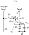
Fig. 2 shows the circuit diagram of an instance of the physical circuit structure of a pixel (image element circuit) 20.Pixel 20 has the illuminating part that comprises organic EL 21, and this organic EL 21 is current drive-type electrooptic cells.The luminosity of organic EL 21 changes according to the current value of flowing through in the device.
As shown in Figure 2, pixel 20 also comprises being used for through making electric current flow into the drive circuit that organic EL 21 drives organic EL 21 except comprising organic EL 21.Organic EL 21 has the cathode electrode that is connected to public power supply line 34, and this public power supply line 34 is connected to all pixels 20 (also being called as " public wiring ").
The drive circuit that is used to drive organic EL 21 has driving transistors 22, writes transistor 23, holding capacitor 24 and auxiliary capacitor 25.Driving transistors 22 with write transistor 23 and can realize by the n-channel TFT.Yet the combination that shown driving transistors 22 writes the conduction type of transistor 23 only is an example, and the combination of conduction type is not limited thereto.In addition, the distribution annexation of transistor, holding capacitor and organic EL device etc. is not limited to disclosed relation.
First electrode (source/drain electrode) of driving transistors 22 is connected to the anode electrode of organic EL 21, and second electrode (source/drain electrode) of driving transistors 22 is connected to power supply line 32 (32
1To 32
m) in corresponding one.
Write transistor 23 first electrodes (source/drain electrode) and be connected to holding wire 33 (33
1To 33
n) in corresponding one, and second electrode (source/drain electrode) that writes transistor 23 is connected to the gate electrode of driving transistors 22.The gate electrode that writes transistor 23 is connected to scan line 31 (31
1To 31
m) in corresponding one.
Driving transistors 22 with write the metal wiring that statement " first electrode " expression in the transistor 23 is electrically connected to source/drain region; Statement " second electrode " expression is electrically connected to Lou/metal wiring in source region.According to the electric potential relation between first electrode and second electrode, first electrode is as source electrode or drain electrode, or second electrode is also as drain electrode or source electrode.
First electrode of holding capacitor 24 is connected to the gate electrode of driving transistors 22, and second electrode of holding capacitor 24 is connected to first electrode of driving transistors 22 and the anode electrode of organic EL 21.
First electrode of auxiliary capacitor 25 is connected to the anode electrode of organic EL 21, and second electrode of auxiliary capacitor 25 is connected to public power supply line 34.Auxiliary capacitor 25 is auxiliary as the equivalent capacity of organic EL 21, thus the deficiency of the device capacitances of compensation organic EL 21, thus and improve the gain that writes for the vision signal of holding capacitor 24.
In this case, though second electrode of auxiliary capacitor 25 is connected to public power supply line 34, second electrode of auxiliary capacitor 25 can be connected to the node of fixed potential, rather than public power supply line 34.Second electrode of auxiliary capacitor 25 is not enough with the electric capacity that being connected of the node of fixed potential can compensate organic EL 21, and can realize the raising that writes gain for the vision signal of holding capacitor 24.
Have and write transistor 23 in response to providing height (that is, to activate, active) write sweep signal WS and get into conducting state from writing scanning circuit 40 in the pixel 20 of above-mentioned structure to the gate electrode that writes transistor 23 through scan line 31.Write the signal voltage V of transistor 23 sample video signals (corresponding to monochrome information) then
SigOr the reference potential V that provides from signal output apparatus 60 through holding wire 33
Ofs, and with the signal voltage V that samples
SigOr reference voltage V
OfsWrite pixel 20.The signal voltage V that writes
SigOr reference voltage V
OfsBe applied to the gate electrode of driving transistors 22 and by holding capacitor 24 storage.
When power supply line 32 (32
1To 32
m) in corresponding one power supply potential DS be the first power supply potential V
CcpThe time, driving transistors 22 is operated in the saturation region, and its first electrode is as drain electrode, and second electrode is as the source electrode.Thereby in response to the electric current that provides from power supply line 32, driving transistors 22 is luminous through providing drive current to drive organic EL 21 to it.More specifically, through the operation in the saturation region, driving transistors 22 provides drive current to organic EL 21, and this drive current has and the corresponding current value V of the magnitude of voltage of holding capacitor 24 signal stored voltages
SigDrive current makes organic EL 21 be actuated to carry out luminous.
When power supply potential DS from the first power supply potential V
CcpSwitch to second source current potential V
IniThe time, driving transistors 22 is as switching transistor, and its first electrode is as the source electrode, and its second electrode is as drain electrode.Through handover operation, driving transistors 22 stops to organic EL 21 drive current being provided, thereby makes organic EL 21 get into non-luminance.That is, driving transistors 22 has and is used to control organic EL 21 luminous and non-luminous transistorized functions.
Driving transistors 22 carry out handover operations with provide organic EL 21 non-luminous during (between non-light emission period), thereby make it possible to control between the light emission period of organic EL 21 and (duty) ratio between non-light emission period.Through duty control, can reduce included after image in during whole display frame pixel 20 luminous.Thereby especially, the picture quality of moving image further improves.
At first and second power supplys supply voltage V that optionally provides from power supply scanning circuit 50 through power supply line 32
CcpAnd V
IniIn, the first power supply potential V
CcpBe to be used for providing to the power supply potential of driving transistors 22 with driving organic EL 21 luminous drive currents.Second source current potential V
IniIt is the power supply potential that is used for reverse bias organic EL 21.Second source current potential V
IniBe set to and be lower than reference voltage V
OfsFor example, second source current potential V
IniBe set to be lower than V
Ofs-V
ThCurrent potential, preferably, be set at far below V
Ofs-V
ThCurrent potential, V wherein
ThThe threshold voltage of expression driving transistors 22.
[operation of 1-2. basic circuit]
Next, will the basic circuit operation of the organic EL display 10 with above-mentioned structure be described with reference to the application drawing shown in the timing waveform figure shown in the figure 3 and Fig. 4 A to Fig. 5 D.In the application drawing shown in Fig. 4 A to Fig. 5 D, write transistor 23 and represent, with simplified illustration by switch symbols.
The timing waveform of Fig. 3 illustrates the variation, the current potential (V of holding wire 33 of current potential (power supply potential) DS of variation, the power supply line 32 of current potential (the writing sweep signal) WS of scan line 31
Sig/ V
Ofs) variation and the grid current potential V of driving transistors 22
gWith source electric potential V
sVariation.(between the light emission period of last display frame)
In the timing waveform figure of Fig. 3, be between the light emission period of organic EL 21 of last display frame during before the time t11.In between the light emission period of last display frame, the current potential DS of power supply line 32 is in first power supply potential (below be called " high potential ") V
Ccp, and write transistor 23 and be in nonconducting state.
Driving transistors 22 be designed to this time in the saturation region, operate.Therefore, shown in Fig. 4 A, with the gate source voltage V of driving transistors 22
GsCorresponding driving electric current (drain-source current) I
DsBe provided to organic EL 21 through driving transistors 22 from power supply line 32.Therefore, the luminosity of organic EL 21 and drive current I
DsCurrent value corresponding.
(threshold value was proofreaied and correct between the preparatory stage)
At time t11, operation has got into new display frame (current display frame) to carry out the line sequential scanning.Shown in Fig. 4 B, the current potential DS of power supply line 32 is from high potential V
CcpSwitch to second source current potential (below be called " electronegative potential ") V
Ini, it is with respect to the reference potential V of holding wire 33
OfsFar below V
Ofs-V
Th
Make V
ThelBe the threshold voltage of organic EL 21, and make V
CathCurrent potential (cathode potential) for public power supply line 34.In this case, at supposition electronegative potential V
IniSatisfy V
Ini<v
Thel+ V
CathThe time, the source electric potential V of driving transistors 22
sBe substantially equal to electronegative potential V
IniTherefore, organic EL 21 is placed in reverse-bias state and stops luminous.
Next, at time t12, the current potential WS of scan line 31 moves to hot side from low potential side, is placed in conducting state thereby write transistor 23, shown in Fig. 4 C.At this point, because reference potential V
OfsBe provided to holding wire 33 from signal output apparatus 60, so the grid current potential V of driving transistors 22
gAs reference potential V
OfsThe source electric potential V of driving transistors 22
sEqual far below reference potential V
OfsCurrent potential V
Ini, promptly equal electronegative potential V
Ini
At this point, the gate source voltage V of driving transistors 22
GsEqual V
Ofs-V
IniIn this case, only if V
Ofs-V
IniThreshold voltage V much larger than driving transistors 22
Th, otherwise be difficult to carry out following threshold value treatment for correcting.Therefore, thus carry out to be provided with and to satisfy V
Ofs-V
Ini>V
ThThe electric potential relation of expressing.
Grid current potential V with driving transistors 22
gFixing (setting) is reference potential V
OfsAnd with source electric potential V
sBe fixed as electronegative potential V
IniInitialization process be to carry out the preparation before of following threshold value treatment for correcting (threshold value correct operation) to handle (threshold value is proofreaied and correct and prepared).Like this, reference potential V
OfsWith electronegative potential V
IniGrid current potential V as driving transistors 22
gWith source electric potential V
sThe initialization current potential.
(during the threshold value correction)
Next, at time t13, the current potential DS of power supply line 32 is from electronegative potential V
IniSwitch to high potential V
Ccp, shown in Fig. 4 D, and work as the grid current potential V of driving transistors 22
gMaintain reference voltage V
OfsThe time, beginning threshold value treatment for correcting.That is the source electric potential V of driving transistors 22,
sBegin to from grid current potential V
gIn deduct the threshold voltage V of driving transistors 22
ThThe current potential that obtains increases.
Here, the grid current potential V of referenced drive transistor 22
gInitialization current potential V
Ofs, with source electric potential V
sTo from initialization current potential V
OfsIn deduct the threshold voltage V of driving transistors 22
ThThe processing of the current potential that is obtained is called " threshold value treatment for correcting " for ease of explanation.When the threshold value treatment for correcting is carried out, the gate source voltage V of driving transistors 22
GsBe arranged to the threshold voltage V of driving transistors 22 at last
ThWith threshold voltage V
ThCorresponding voltage is by holding capacitor 24 storages.
Carry out the threshold value treatment for correcting during in (that is, during threshold value is proofreaied and correct in), the current potential V of public power supply line 34
CathBe provided so that organic EL 21 is placed in cut-off state, thereby make electric current flow into holding capacitor 24, and prevent that electric current from flowing into organic EL 21.
Next, at time t14, the current potential WS of scan line 31 moves to low potential side, is placed in nonconducting state thereby write transistor 23, shown in Fig. 5 A.At this point, the gate electrode of driving transistors 22 separates with holding wire 33 electricity, thereby the gate electrode of driving transistors 22 gets into floating state.Yet, because gate source voltage V
GsEqual the threshold voltage V of driving transistors 22
ThSo driving transistors 22 is in cut-off state.Thus, almost there is not drain-source current I
DsFlow into driving transistors 22.
(signal write proofread and correct with mobility during)
Next, at time t15, shown in Fig. 5 B, the current potential of holding wire 33 is from reference potential V
OfsSwitch to the signal voltage V of vision signal
SigAfter this, shown in Fig. 5 C, at time t16, the current potential WS of scan line 31 moves to hot side, gets into conducting state thereby write transistor 23, thus the signal voltage V of sample video signal
SigAnd with signal voltage V
SigWrite pixel 20.
At this point, organic EL 21 is in cut-off state (high impedance status).Thus, according to the signal voltage V of vision signal
SigFlow into electric current (the drain-source current I of driving transistors 22 from power supply line 32
Ds) flow into the equivalent condenser and the auxiliary capacitor 25 of organic EL 21.Thereby the charging of the equivalent condenser of organic EL 21 and auxiliary capacitor 25 begins.
As the result of the equivalent condenser of organic EL 21 and auxiliary capacitor 25 chargings, along with driving transistors 22 source electric potential V time lapse
sIncrease.Because the threshold voltage V of the driving transistors of pixel 22
ThVariation be cancelled at this point, so the drain-source current I of driving transistors 22
DsThe mobility [mu] that depends on driving transistors 22.The mobility [mu] of driving transistors 22 refers to the mobility of the semiconductive thin film in the raceway groove that is included in driving transistors 22.
The voltage V that supposition is now stored by holding capacitor 24
GsSignal voltage V with vision signal
SigRatio (this ratio is called " writing gain G ") be 1 (ideal value).In this case, the source electric potential V of driving transistors 22
sBe increased to by V
Ofs-V
ThThe current potential that+Δ V expresses, thereby the gate source voltage V of driving transistors 22
GsReach by V
Sig-V
Ofs+ V
ThThe value that-Δ V expresses.
That is 22 source electric potential V of driving transistors,
sIncrease Δ V work so that its voltage (V that stores from holding capacitor 24
Sig-V
Ofs+ V
Th) middle being deducted, make that promptly the electric charge in the holding capacitor 24 is discharged.In other words, will with source electric potential V
sThe corresponding negative feedback of increase Δ V be applied to holding capacitor 24.Like this, source electric potential V
sIncrease Δ V corresponding with degenerative amount.
When having and the drain-source current I that flows into driving transistors 22
DsThe negative feedback of corresponding degenerative amount Δ V is applied in gate source voltage V in the above described manner
GsThe time, can eliminate the drain-source current I of driving transistors 22
DsDependence to mobility [mu].This processing that is used to cancel to the dependence of mobility [mu] is the mobility treatment for correcting that is used to proofread and correct the variation of the mobility [mu] of the driving transistors 22 of each pixel.
More particularly, write the signal amplitude V of vision signal of the gate electrode of driving transistors 22
In(=V
Sig-V
Ofs) high more, drain-source current I
DsBig more.Like this, the absolute value of degenerative amount Δ V also increases.Therefore, carry out the mobility treatment for correcting according to the luminosity level.
Signal amplitude V when vision signal
InWhen constant, the absolute value of degenerative amount Δ V is along with the mobility [mu] of driving transistors 22 increases.Therefore, the variation of the mobility [mu] of each pixel can reduce or eliminate.That is, degenerative amount Δ V also is called as " correcting value of mobility treatment for correcting ".The details explanation of the principle that mobility is proofreaied and correct as follows.
(between light emission period)
Next, at time t17, the current potential WS of scan line 31 moves to low potential side, is placed in nonconducting state thereby write transistor 23, shown in Fig. 5 D.Therefore, the gate electrode of driving transistors 22 separates with holding wire 33 electricity, thereby the gate electrode of driving transistors 22 gets into floating state.
In this case, when the gate electrode of driving transistors 22 is in floating state, because holding capacitor 24 is connected between the grid and source electrode of driving transistors 22, so grid current potential V
gAlso with the source electric potential V of driving transistors 22
sVariation interlock ground change.
The grid current potential V of driving transistors 22
gWith source electric potential V
sThis operation that changes of variation interlock ground, promptly ought keep the gate source voltage V of storage in the holding capacitor 24
GsThe time, grid current potential V
gWith source electric potential V
sThe operation that increases is called as " bootstrapping operation " in this article.
When the gate electrode of driving transistors 22 gets into floating state, the drain-source current I of driving transistors
Ds22 begin to flow into organic EL 21, thereby the anode potential of organic EL 21 is in response to drain-source current I
DsAnd increase.
When the anode potential of organic EL element 21 surpasses V
Thel+ V
CathThe time, drive current begins to flow into organic EL 21, thereby makes organic EL 21 beginnings luminous.The increase of the anode potential of organic EL 21 is because the source electric potential V of driving transistors 22
sIncrease.Source electric potential V when driving transistors 22
sDuring increase, the bootstrapping of holding capacitor 24 operation makes the grid current potential V of driving transistors 22
gWith source electric potential V
sInterlock ground increases.
When the gain of boostrap circuit is assumed to 1 (ideal value), grid current potential V
gRecruitment equal source electric potential V
sRecruitment.Therefore, between light emission period in, the gate source voltage V of driving transistors 22
GsThe constant V that maintains
Sig-V
Ofs+ V
Th-Δ V.At time t18, the current potential of holding wire 33 is from the signal voltage V of vision signal
SigSwitch to reference voltage V
Ofs
In above-mentioned a series of circuit operations, threshold value is proofreaied and correct and is prepared, threshold value is proofreaied and correct, signal voltage V
SigThe processing that (signal writes) and mobility proofread and correct of writing operate in the horizontal scan period (1H) and carry out.Signal writes the processing of proofreading and correct with mobility and operates in time t16 and carry out concurrently in during the time t17.
[segmentation threshold correction]
Though provided the explanation that utilizes the instance of only carrying out threshold value treatment for correcting driving method once above, this driving method only is an example, nor is limited to this.For example also can adopt the driving method that is used for carrying out so-called " segmentation threshold correction ".In segmentation threshold is proofreaied and correct; Except that with mobility proofread and correct write during the 1H that handles interlock ground execution threshold value treatment for correcting with signal; Before during the 1H, repeatedly carry out the threshold value treatment for correcting, promptly in a plurality of horizontal scan period, carry out the threshold value treatment for correcting with partitioning scheme.
Through the driving method that segmentation threshold is proofreaied and correct,, also can in a plurality of scan periods during the threshold value correction, guarantee the time enough amount even when the time of distributing to a horizontal scan period reduces owing to more high-resolution pixel quantity increases.Therefore, even because during can guaranteeing also that when distributing to the time decreased of a horizontal scan period time enough amount is proofreaied and correct as threshold value, so can carry out the threshold value treatment for correcting reliably.
[principle that threshold value is eliminated]
The threshold value that driving transistors 22 will be described is now eliminated and (is offset, cancellation) principle of (being that threshold value is proofreaied and correct).Because driving transistors 22 is designed in the saturation region, operate, so it is as constant current source.Therefore, a certain amount of drain-source current (drive current) I
DsFlow to organic EL 21 from driving transistors 22, and be given:
I
ds=(1/2)·μ(W/L)C
ox(V
gs-V
th)
2 (1)
Wherein, w representes the channel width of driving transistors 22, and L representes channel length, C
OxThe gate capacitance of expression per unit area.
Fig. 6 A shows the drain-source current I of driving transistors 22
DsTo gate source voltage V
GsThe diagrammatic sketch of characteristic.Shown in Fig. 6 A, if not to the threshold voltage V of the driving transistors 22 of each pixel
ThVariation carry out to eliminate handle (treatment for correcting), then as threshold voltage V
ThBe V
Th1The time, corresponding to gate source voltage V
GsDrain-source current I
DsBecome I
Ds1
On the contrary, as threshold voltage V
ThBe V
Th2(V
Th2>V
Th1) time, corresponding to identical gate source voltage V
GsDrain-source current I
DsBecome I
Ds2(I
Ds2<i
Ds1).That is, at the threshold voltage V of driving transistors 22
ThDuring variation, even as gate source voltage V
GsWhen constant, drain-source current I
DsAlso change.
On the other hand, in having the pixel of above-mentioned structure (image element circuit) 20, as stated, the gate source voltage V of the driving transistors 22 between light emission period
GsBe expressed as V
Sig-V
Ofs+ V
Th-Δ V.Like this, this expression formula is updated to above-mentioned equality (1) and generates the drain-source current Ids that provides as follows:
I
ds=(1/2)·μ(W/L)C
ox(V
sig-V
ofs-ΔV)
2 (2)
That is the threshold voltage V of driving transistors 22,
Thbe eliminated, make the drain-source current I that is provided to organic EL 21 from driving transistors 22
DsThe threshold voltage V that does not depend on driving transistors 22
ThTherefore, even work as the threshold voltage V of driving transistors 22
ThSince the variation that driving transistors 22 manufacturing is handled, aging etc. when changing for each pixel, drain-source current I
DsAlso constant.Therefore, the luminosity of organic EL 21 can be kept constant.
[principle that mobility is proofreaied and correct]
Next the principle of the mobility correction of driving transistors 22 will be described.Fig. 6 B shows the diagrammatic sketch of the indicatrix of the comparison between the less pixel B of the mobility [mu] of bigger pixel A of the mobility [mu] of driving transistors 22 and driving transistors 22.When driving transistors 22 is realized through multi-crystal TFT etc., the variation of the mobility [mu] of pixel takes place, as among pixel A and the B.
Provide the explanation of such instance now, wherein, when the mobility [mu] of A in the pixel and B changes, the signal amplitude V of same level
In(=V
Sig-V
Ofs) be written into the gate electrode of the driving transistors 22 of pixel A and B.In this case, if mobility [mu] carry out is not proofreaied and correct, then at the drain-source current I of pixel A that flows through with big mobility [mu]
Ds1' with the drain-source current I of the pixel B of flowing through with little mobility [mu]
Ds2' between produce big difference.When because the variation of the mobility [mu] of pixel and at the drain-source current I of pixel
DsBetween when producing big difference, image evenness is damaged.
As above-mentioned equality (1) given transistor characteristic showed, drain-source current I
DsAlong with mobility [mu] increases and increases.Therefore, along with mobility [mu] increases, degenerative amount Δ V increases.Shown in Fig. 6 B, has the degenerative amount Δ V of the pixel A of big mobility [mu]
1Degenerative amount Δ V greater than pixel B with little mobility [mu]
2
Therefore, when carrying out the mobility treatment for correcting, make the drain-source current I that will have with driving transistors 22
DsThe negative feedback of the amount Δ V of corresponding feedback is applied to gate source voltage V
GsThe time, along with mobility [mu] increases, apply bigger amount of negative feedback.Therefore, can suppress the variation of the mobility [mu] of pixel.
More specifically, when the pixel A with big mobility [mu] is carried out and degenerative amount Δ V
1Corresponding timing, drain-source current I
DsSignificantly from I
Ds1' be reduced to I
Ds1On the other hand, because have the amount Δ V of the feedback in the pixel B of less mobility [mu]
2Less, so drain-source current I
DsFrom I
Ds2' be reduced to I
Ds2, and this decrease is so not big.Therefore, the drain-source current I of pixel A
Ds1Drain-source current I with pixel B
Ds2Becoming is equal to each other basically, thereby the variation of the mobility [mu] of pixel is able to proofread and correct.
In brief, when existence has pixel A and the B of different mobility [mu], has the feedback quantity Δ V of the pixel A of big mobility [mu]
1Feedback quantity Δ V greater than pixel B with less mobility [mu]
2That is, the mobility [mu] of pixel is big more, and feedback quantity Δ V is big more, and drain-source current I
DsDecrease is big more.
Therefore, owing to will have the drain-source current I with driving transistors 22
DsThe negative feedback of corresponding feedback quantity Δ V is applied to gate source voltage V
Gs, make the drain-source current I of pixel with different mobility [mu]
DsCurrent value become and be equal to each other.The variation of mobility [mu] that therefore, can correction pixels.That is, the mobility treatment for correcting is such processing, wherein, and to the gate source voltage V of driving transistors 22
Gs, promptly apply electric current (the drain-source current I that has with inflow driving transistors 22 to holding capacitor 24
Ds) negative feedback of corresponding feedback quantity (correcting value) Δ V.Above-mentioned threshold value is proofreaied and correct and proofreaied and correct with mobility is the operation that can carry out in the present invention or not carry out, and above-mentioned various corrections, luminous etc. is not limited to these operations and timing.
[1-3. bottom grating structure and top gate structure]
In the organic EL display with above-mentioned structure 10, the transistor in the pixel 20 specifically, constitutes driving transistors 22 and the TFT that writes transistor 23, is divided into bottom grating structure and top gate structure widely according to structure.In bottom grating structure, gate electrode is positioned at respect to semiconductor layer more near a side of substrate.In top gate structure, gate electrode is positioned at the opposition side with respect to the semiconductor layer substrate.
When having bottom grating structure TFT as the transistor in the pixel 20, semiconductor layer and thin dielectric membrane are between the metal level of the metal level of gate electrode and source/drain electrode.Therefore, the metal level of gate electrode and the metal level of source/drain electrode are configured to against each other, make to utilize thin dielectric membrane to form between metal level as dielectric capacitor.The film formed capacitor of insulation that between these metal levels, utilizing is situated between therebetween has can be as making the capacity cell in the pixel 20, for example, as auxiliary capacitor 25, auxiliary with as the equivalent condenser of organic EL 21.
On the other hand; When the TFT with top gate structure is used as the transistor in the pixel 20; Form the insulation planarization film in the circuit part of transistor etc. comprising, thus the top of this circuit part of planarization, and on the insulation planarization film metal level of formation source/drain electrode.Transistor in the pixel 20 is that the situation of driving transistors 22 will illustrate in greater detail with reference to figure 7.
As shown in Figure 7, go up the semiconductor layer 221 that forms driving transistors 22 at substrate (for example glass substrate 71).The center of semiconductor layer 221 is as channel region 222, and the opposite end of channel region 222 is as source/drain region 223 and 224.Deposition gate insulating film 225 on the channel region 222 of semiconductor layer 221, and on gate insulating film 225, form gate electrode 226.
The top of TFT circuit part that comprises the driving transistors 22 of formation like this for planarization forms insulation planarization film 72 comprising in the TFT circuit part of driving transistors 22. Contact hole 73 and 74 forms in insulation planarization film 72, thereby is communicated with the corresponding source/ drain region 223 and 224 of the opposite end of semiconductor layer 221.Source/ drain electrode 227 and 228 forms on insulation planarization film 72, and contact hole 73 and 74 is filled with wiring material (electrode material), thereby source/ drain electrode 227 and 228 is electrically connected with source/ drain region 223 and 224 respectively.
As stated, when the transistor of pixel 20 was realized by the TFT with top gate structure, insulation planarization film 72 mainly was provided for planarization.Therefore, the thickness of insulation planarization film 72 is significantly greater than the thickness of gate insulating film 225.The big thickness of insulation planarization film 72 makes and is difficult between the metal level of the metal level of gate electrode 226 and source/ drain electrode 227 and 228, form capacitor.
Because like this, if the capacity cell that system is gone in the pixel 20 can be formed in the zone the zone between these metal levels, then can improve the degree of freedom of the cross section structure of pixel 20.Not only be used as under the transistorized situation in the pixel 20, and be used as under the transistorized situation in the pixel 20 at TFT with bottom grating structure at TFT with top gate structure, so same.
2. execution mode
The degree of freedom for the cross section structure that improves pixel 20; Execution mode of the present invention adopts such structure; Wherein, make capacity cell in the pixel 20 is formed on and transistorized gate electrode with the metal level of one deck be formed with between the semiconductor layer in transistorized source/drain region.The formation of the capacity cell between metal level and the semiconductor layer relates to metal level is applied voltage.Referring now to Fig. 8 A to Fig. 8 C, thereby explain why voltage is applied to metal level forms capacity cell between metal level and semiconductor layer reason.
Fig. 8 A shows C-V (capacitance voltage) characteristic such as semiconductor layer and metal level during the high frequencies of operation of the operation of driving pixels 20.In the C-V of Fig. 8 A characteristic, transverse axis is represented the current potential of metal level with respect to semiconductor layer.The longitudinal axis is represented ratio C/C
0, C wherein
0The electric capacity of expression gate insulating film, C representes the electric capacity between metal level and the semiconductor layer.
In the C-V of Fig. 8 A characteristic, the C/C at the some A place that the indicatrix and the longitudinal axis intersect
0Provide as follows:
A(C/C
0)=1/{1+K
0L
D/(K
td)}
Wherein, K
0The relative dielectric constant of expression gate insulating film, td representes the thickness of gate insulating film, K representes semi-conductive relative dielectric constant, and L
DThe screening range of expression charge carrier.
To be the transistorized situation of N-channel MOS through the transistor that example is discussed in the pixel 20 now.
For the N-channel MOS transistor, when being applied to metal level with respect to the sufficiently high voltage of the voltage of semiconductor layer, electronics promptly, forms raceway groove on the surface of semiconductor layer, shown in Fig. 8 B (corresponding to the state 1 shown in Fig. 8 A) in the cumulative of semiconductor layer.Therefore, the gate insulating film that is folded between semiconductor layer and the metal level is used as dielectric to form capacitor.That is the voltage that, can form the raceway groove of q.s on the surface of semiconductor layer is applied to metal level.
In the C-V of Fig. 8 A characteristic, V
1Expression makes the capacitor C of gate insulating film
0The magnitude of voltage that becomes visible, in other words, expression is as the capacitor C of dielectric gate insulating film
0Becoming the magnitude of voltage that equals the capacitor C between metal level and the semiconductor layer (is C/C
0=1).On the other hand, when the low voltage with respect to the voltage of semiconductor layer is applied to metal level, increase at the area of the surface electronic depletion region of semiconductor layer, shown in Fig. 8 B (it is corresponding to the state 2 shown in Fig. 8 A).This reduces to form between semiconductor layer and the metal level and use the capacitance of gate insulating film as dielectric capacitor.
Above-mentioned showing, at metal level with semiconductor layer is configured to against each other and gate insulating film is folded in the dot structure therebetween, metal level is applied voltage can make the surface of semiconductor layer form raceway groove.This makes it possible to use gate insulating film to form capacitor as dielectric.For example, capacitor can further be used as will make the capacity cell in the pixel 20, for example, and the auxiliary capacitor 25 in the image element circuit as shown in Figure 2.Through this configuration, because the capacity cell that will make in the pixel 20 can form in the zone the zone between metal level, so can improve the degree of freedom of the cross section structure of pixel 20.
Fig. 9 shows the sectional view of the cross section structure of pixel according to the embodiment of the present invention.Fig. 9 shows the driving transistors 22 and auxiliary capacitor 25 of the image element circuit shown in Fig. 2, promptly shows to be formed on the instance that is used as auxiliary capacitor 25 between metal level and the semiconductor layer and with gate insulating film as dielectric capacitor.In Fig. 9, with same part among Fig. 7 with same reference number mark.
As stated, with reference to figure 7, comprise that the TFT circuit part of driving transistors 22 is formed on the glass substrate 71.Driving transistors 22 comprises, be formed on semiconductor layer 221 on the glass substrate 71, and the gate electrode 226 that is oppositely arranged of the channel region 222 of semiconductor layer 221 and place semiconductor layer 221 and gate electrode 226 between gate insulating film 225.In semiconductor layer 221, the opposite end of channel region 222 is used separately as source/ drain region 223 and 224.
Comprising formation insulation planarization film 72 in the TFT circuit part of driving transistors 22, thus its top of planarization.On insulation planarization film 72, form the wiring layer that comprises source/drain electrode 227 and 228.In this example, the source/drain electrode 228 in a side of driving transistors 22 also is suitable for the anode electrode as organic EL 21.On the wiring layer that comprises source/ drain electrode 227 and 228, form window dielectric film 75.Form the organic layer (not shown) of organic EL 21 in the peristome in window dielectric film 75 (recess) 76, and on window dielectric film 75, form the cathode electrode (not shown, all pixels are shared) of organic EL 21.
In having the dot structure of above-mentioned structure, semiconductor layer 221 is set in organic EL 21 bottoms, extend.One end of semiconductor layer 221, promptly source-drain electrode 224, also are used as first electrode 251 of auxiliary capacitor 25.Second electrode 252 of auxiliary capacitor 25 with same one deck of the layer of the gate electrode 226 of driving transistors 22 in form, thereby relative with first electrode 251.Between first electrode 251 and second electrode 252, gate insulating film 253 is set.
As stated, make the voltage that promptly forms the raceway groove of q.s on the surface of semiconductor layer 221 be applied to second electrode 252 as metal level on the surface of first electrode 251.Therefore, electronics will be made the capacity cell in the pixel 20 thereby use gate insulating film 253 to form to be used as as dielectric capacitor, promptly as the auxiliary capacitor 25 in this instance in the cumulative of semiconductor layer 221.
The situation that first electrode 251 that auxiliary capacitor 25 is described below with reference to the embodiment that voltage is applied to second electrode 252 is realized by semiconductor layer 221 and second electrode 252 of auxiliary capacitor 25 is realized by metal level.
[2-1. first execution mode]
Figure 10 is the circuit diagram according to the image element circuit of first execution mode.In Figure 10, represent with same reference number with those the same parts among Fig. 2.
Image element circuit according to first execution mode adopts following structure; Wherein, Second electrode of auxiliary capacitor 25 is public power supply lines 34 open circuit rather than that be connected to earth level, and it is different from the situation of the image element circuit shown in Fig. 2, and constant voltage V
SubBe applied to second electrode from the external power source (not shown).
Figure 11 shows and is used for constant voltage V
SubBe applied to the layout instance of panel of second electrode of auxiliary capacitor 25 from the power supply of outside.Shown in figure 11, voltage supply line L
1Be connected to second electrode of auxiliary capacitor 25 in the image element circuit with behavior unit.Voltage supply line L
1Outer part in pixel array unit 30 is arrived together by harness, thereby forms the public power supply line L that for example centers on the ring-type of pixel array unit 30
2Pad PAD
1And PAD
2Opposite end (left and right end portions) at panel forms, and is connected to the public power supply line L of ring-type
2Through pad PAD
1And PAD
2, public power supply line L
2With voltage supply line L
1With constant voltage V
SubBe provided to second electrode of auxiliary capacitor 25 from the external power source (not shown) of panel.
Utilize the pad PAD that passes through in the opposite end of panel
1And PAD
2Voltage is applied to the public power supply line L of ring-type
2Configuration, constant voltage V
SubCan stably be provided to second electrode of the auxiliary capacitor 25 in the pixel.This configuration can reduce the capacitance C of the auxiliary capacitor 25 in the pixel
SubVariation, thereby image element circuit can be by the stable capacitance value C of auxiliary capacitor 25
SubDrive.
In this case, preferably, during high grade grey level (high-gradation) vision signal, the constant voltage V that the outside provides
SubSource electric potential with respect to driving transistors 22 has above-mentioned magnitude of voltage V
1(that is, make the capacitor C of gate insulating film
0The magnitude of voltage that becomes visible) or bigger value.If the current potential (being the current potential of metal level) with respect to second electrode of the auxiliary capacitor 25 of the source electric potential (being the current potential of semiconductor layer) of driving transistors 22 reduces, then the capacitance C of auxiliary capacitor 25
SubReduce, thereby the luminosity of pixel 20 reduces.
Referring now to the timing waveform figure shown in Figure 12, the mechanism that brightness reduces is described when the current potential with respect to the metal level of the current potential of semiconductor layer reduces.
When write at signal proofread and correct with mobility during the capacitance C of auxiliary capacitor 25
SubUnder the situation less than designated value, as the signal voltage V of vision signal
SigSource voltage V when writing the grid of driving transistors 22
sIncrease become big, shown in the dotted line of Figure 12.Therefore, be right after the gate source voltage V of luminous driving transistors 22 before
GsReduce, thereby the brightness of organic EL 21 reduces.
Make C
OledBe the capacitance of the equivalent capacity of organic EL 21, and make C
sBe the capacitance of holding capacitor 24, the source voltage V of the driving transistors 22 during signal writes
sRecruitment Δ V
sProvide as follows:
ΔV
s=(V
sig-V
ofs)/(C
s+C
sub+C
oled)
If the capacitance C of auxiliary capacitor 25
SubBetween light emission period, significantly change to little capacitance from big capacitance; The same effect of the effect of the situation that this will cause changing to the depletion type characteristic with the characteristic of organic EL 21 (yet; Image element circuit according to first execution mode is no problem, because it is suitable for constant voltage V
SubBe applied to the mode of second electrode of auxiliary capacitor 25).Therefore, the operating point of each organic EL 21 changes.Brightness irregularities takes place in the result as the operating point of the organic EL in the pixel 21 changes.
Cause the mechanism of brightness irregularities referring now to the variation of the operating point of the organic EL 21 in Figure 13 and Figure 14 pixels illustrated.
Shown in figure 13, the capacitance characteristic of semicoductor capacitor is capacitance V near threshold voltage
ThThe point place that significantly changes through voltage is variable.Therefore, at the voltage V of second electrode of auxiliary capacitor 25
SubWith respect to the current potential of semiconductor layer, promptly with respect to the source electric potential V of driving transistors 22
sNear threshold voltage V
ThThe time, the capacitance C of auxiliary capacitor 25
SubBig pixel and capacitance C
SubLittle pixel coexists in same panel.In Figure 13, the capacitance C of auxiliary capacitor 25
SubThe characteristic of big pixel is represented with chain-dotted line, and the capacitance C of auxiliary capacitor 25
SubThe characteristic of little pixel is represented with double dot dash line.
Capacitance C for auxiliary capacitor 25
SubBig pixel is because the source voltage V of driving transistors 22
sRecruitment little, so brightness increase, shown in the chain-dotted line of Figure 14.On the contrary, for the capacitance C of auxiliary capacitor 25
SubLittle pixel is because the source voltage V of driving transistors 22
sRecruitment big, so brightness reduce, shown in the double dot dash line of Figure 14.Therefore, coexist in same panel owing to have the pixel of high brightness and have the low-light level pixel, so the variation of brightness is observed to the inhomogeneous of brightness.
[2-2. second execution mode]
Next image element circuit according to second execution mode will be described.Image element circuit according to second execution mode adopts and the same circuit structure of the image element circuit according to first execution mode shown in Figure 10.That is second electrode of auxiliary capacitor 25 open circuit.Although the image element circuit according to above-mentioned first execution mode is used for making constant voltage V
SubSecond electrode to auxiliary capacitor 25 is provided, but adopts pulse voltage V according to the image element circuit of second execution mode
SubBe applied to the structure of second electrode of auxiliary capacitor 25.
More specifically, needing the capacitance C of auxiliary capacitor 25
SubKeep bigger during, pulse voltage V
SubIncrease to high voltage V
H, shown in the timing waveform among Figure 15.Above-mentioned explanation shows, during the high grade grey level vision signal writes, and high voltage V
HSource electric potential with respect to driving transistors 22 has magnitude of voltage V
1Or bigger value.The capacitance C that needs auxiliary capacitor 25
SubKeep during bigger is that the current potential DS of power supply line 32 is first power supply potential V
CcpDuring.Needing the capacitance C of auxiliary capacitor 25
SubKeep bigger during beyond during, pulse voltage V
SubBe reduced to low-voltage V
L
When voltage was applied to metal level continuously, the characteristic of the capacitor that between semiconductor layer and metal level, forms changed the enhancement mode characteristic into, thereby reliability possibly reduce.In addition, because characteristic is also different because of pixel to the speed that the enhancement mode characteristic changes, so the difference of speed causes the variation of the capacitance of pixel.
Because like this, with voltage V
SubChopping, thus make voltage be applied to metal level discontinuously, in other words, make the voltage application time minimization at auxiliary capacitor 25 two ends, thereby make it possible to guarantee the reliability of auxiliary capacitor 25.
Especially, during organic EL 21 is non-luminous, the source electric potential V of driving transistors 22
sBecome the second source current potential V of the current potential DS of power supply line 32
IniThereby, the low-voltage V of pulse voltage Vsub
LAs second source current potential V
IniAs stated, needing the capacitance C of auxiliary capacitor 25
SubKeep bigger during beyond during, the current potential of second electrode of auxiliary capacitor 25 is reduced to second source current potential V
IniThereby, make the voltage at auxiliary capacitor 25 two ends reach 0V.Because the reliability of auxiliary capacitor 25 can be further guaranteed in this configuration, so can prevent that the reliability of capacitor from reducing the even brightness of the brightness disproportionation that causes and reducing.
Figure 16 shows the exemplary driver timing waveform figure regularly according to second execution mode.Figure 16 shows with respect to current potential (sweep signal) WS of the scan line 31 of two pixel columns (line) (i.e. (i-1) pixel column and i pixel column), the current potential DS and the pulse voltage V of power supply line 32
SubWaveform.
Shown in figure 16, expectation pulse voltage V
SubFor each bar line (each row) skew 1H (horizontal period), thus synchronous with the corresponding current potential DS of power supply line 32.As stated, pulse voltage V
SubHigh voltage V
HThe source electric potential that during the high grade grey level vision signal writes, is set to respect to driving transistors 22 has magnitude of voltage V
1The perhaps voltage of bigger value, and low-voltage V
LBe used as the second source current potential V of the current potential DS of power supply line 32
Ini
Figure 17 shows and is used to provide pulse voltage V
SubTo second electrode of auxiliary capacitor 25 and be used to realize instance according to the exemplary driver panel structure regularly of second execution mode.
Shown in figure 17, except that writing scanning circuit 40, for example, on display floater 70, be provided for generating the capacitor generation scanning circuit 80 of auxiliary capacitor 25 with the power supply scanning circuit 50.It is synchronous, synchronous with the current potential DS of power supply line 32 particularly with the operation of power supply scanning circuit 50 that capacitor generates scanning circuit 80, thus in scanning element row sequentially voltage pulse output V sequentially
Sub1To V
SubmThereby, through scan line 35
1To 35
mWith voltage V
Sub1To V
SubmSecond electrode of the auxiliary capacitor 25 to the pixel 20 is provided.
(modification of second execution mode)
Though second execution mode adopts the capacitor of the special use be provided for generating auxiliary capacitor 25 to generate scanning circuit 80 to realize providing pulse voltage V
SubGive the exemplary driver timing of second electrode of auxiliary capacitor 25, but also can adopt following structure as modification.That is, from using pulse voltage V
SubViewpoint, also can adopt such structure, wherein shown in figure 18, the current potential DS of power supply line 32 that belongs to last pixel column (previous row that promptly is right after) is as pulse voltage V
SubProvide.This structure can be connected to the power supply line 32 that belongs to last pixel column and realize through second electrode with auxiliary capacitor 25.
This is because during the high grade grey level vision signal write, the high potential of the current potential DS of each power supply line 32 had magnitude of voltage V with respect to the source electric potential of driving transistors 22
1Or bigger value, the electronegative potential of the current potential DS of power supply line 32 is second source current potential V
IniThereby the current potential DS of power supply line 32 satisfies above-mentioned voltage V
SubThe condition of current potential.In this case, be applied to the voltage V of second electrode of auxiliary capacitor 25
SubTiming have departing from of 1H with respect to the timing under the situation of second execution mode.Yet, when departing from of this 1H is set to enough little and can ignores, substantially the same advantage under the situation with second execution mode can be provided.
3. application examples
Though the instance of the image element circuit of the present invention's be applied to have two transistors (be driving transistors 22 with write transistor 23) and two capacity cells (being holding capacitor 24 and auxiliary capacitor 25) has been described in the above-described embodiment, and application of the present invention is not limited to image element circuit.That is, the present invention is applicable to more substantial transistorized image element circuit being arranged, having the image element circuit of more substantial capacity cell etc.
Though explained in the above-described embodiment that the present invention is applied to the instance of organic EL display, application of the present invention is not limited to this.More particularly, the present invention is applicable to the display unit of using the current drive-type electrooptic cell (light-emitting component) that luminosity changes according to the current value that flows through such as the device of organic EL, LED element and semiconductor laser component.Except the display unit of such use current drive-type electrooptic cell, the present invention also is applicable to the display unit that is employed in the structure that capacity cell is set in the pixel.The instance of such display unit comprises liquid crystal indicator and plasm display device.
4. electronic equipment
Above-mentioned display unit according to the embodiment of the present invention is applicable to the display unit (display unit) of the electronic equipment of every field, wherein, is input to the vision signal of electronic equipment or is shown by the vision signal of its generation form with image or video.For example, shown in Figure 19 to Figure 23 G, the present invention is applicable to such as television set, digital camera, video camera, notebook-sized personal computer and such as the display unit of various types of electronic equipments of the mobile terminal apparatus of mobile phone.
The explanation of above execution mode shows; Display unit according to the embodiment of the present invention can be guaranteed will make the reliability of the capacity cell in the pixel during the capacity cell between metal level and semiconductor layer forms, thereby makes it can prevent that the even brightness of brightness disproportionation from reducing.Thereby display unit according to the embodiment of the present invention can provide high-quality display image as the display unit of the electronic equipment of every field.
Display unit according to the embodiment of the present invention can also realize through the modular form with hermetically-sealed construction.For example, modular form is corresponding to the formed display module of subtend portion through being processed by clear glass etc. to the pixel array unit lamination.For example, display module can also be provided be used for to/from the FPC (flexible print circuit) or the circuit part of the outside input/output signal of pixel array unit etc.
The instantiation of the electronic equipment of using embodiment of the present invention will be described below.
Figure 19 shows the perspective view of the outward appearance of the television set of using embodiment of the present invention.Comprise according to television set that should use-case have front panel 102, the video display frame portion 101 of filter glass 103 etc.This television set is made as video display frame portion 101 according to the display unit of embodiment of the present invention through using.
Figure 20 A and Figure 20 B show the front perspective view and the rear view of the outward appearance of the digital camera of using embodiment of the present invention respectively.Digital camera according to should use-case comprises photoflash lamp illuminating part 111, display part 112, menu switch 113, shutter release button 114 etc.This digital camera is made as display part 112 according to the display unit of embodiment of the present invention through using.
Figure 21 shows the perspective view of the outward appearance of the notebook-sized personal computer of using embodiment of the present invention.Notebook-sized personal computer according to should use-case has following structure, wherein, master unit 121 comprise operation of being used for input character etc. keyboard 122, be used for the display part 123 of display image etc.This notebook-sized personal computer is made as display part 123 according to the display unit of embodiment of the present invention through using.
Figure 22 shows the perspective view of the outward appearance of the video camera of using embodiment of the present invention.Video camera according to should use-case comprises master unit 131, is arranged on the object taking lens 132 of its front side surface, the startup/shutdown switch 133 that is used to take pictures, display part 134 etc.This video camera is made as display part 134 according to the display unit of embodiment of the present invention through using.
Figure 23 A to Figure 23 G shows the external view of the mobile terminal apparatus (for example, mobile phone) of using embodiment of the present invention.Particularly, Figure 23 A is the front view of mobile phone when opening, and its end view of Figure 23 B, Figure 23 C are the front view of mobile phone when closing, and Figure 23 D is a left side view, and Figure 23 E is a right side view, and Figure 23 F is a top view, and Figure 23 G is a bottom view.Mobile phone according to should use-case comprises upper shell 141, lower house 142, joint portion (in this situation, being the articulated section) 143, display 144, slave display 145, picture lamp 146, camera 147 etc.Use according to mobile phone that should use-case and to make as display 144 and/or sub-display 145 according to the display unit of embodiment of the present invention.
< structure 5. of the present invention >
(1) a kind of display unit comprises:
Have electrooptic cell and transistorized pixel, each pixel have and said transistorized gate electrode with the metal level of one deck and be formed with between the semiconductor layer in said transistorized source region and drain region through applying the capacity cell that voltage forms to said metal level.
(2) according to (1) described display unit, wherein, the said voltage that is applied to said metal level can form raceway groove on the surface of said semiconductor layer.
(3) according to (2) described display unit, wherein, the magnitude of voltage that voltage had that is applied to said metal level is more than or equal to satisfying C/C
0=1 magnitude of voltage, wherein, C
0Represent the dielectric electric capacity between said metal level and the said semiconductor layer, C representes the electric capacity between said metal level and the said semiconductor layer.
(4) according to each the described display unit in (1) to (3), wherein, each capacity cell is auxiliary as the equivalent capacity of corresponding electrooptic cell.
(5) according to (4) described display unit, wherein, the corresponding electrooptic cell of each transistor AND gate is connected in series and acts on the driving transistors that drives said electrooptic cell to use; And
Each capacity cell has first electrode of the source/drain electrode that is connected to said driving transistors.
(6) according to (5) described display unit, wherein, each capacity cell has second electrode of the constant voltage of being applied in, and said constant voltage is as the voltage that will be applied to the corresponding metal layer.
(7) according to (6) described display unit, wherein, said pixel is configured to constitute pixel array unit by matrix form; And
The voltage supply line of said second electrode of said constant voltage through being connected to said capacity cell with behavior unit is applied to said second electrode of said capacity cell.
(8) according to (7) described display unit; Wherein, The voltage supply line of said second electrode that is connected to said capacity cell with behavior unit at the outer part of said pixel array unit by harness, to form ring-type common electric voltage supply line around said pixel array unit; And
Said constant voltage is applied to said second electrode of said capacity cell through said ring-type common electric voltage supply line and said voltage supply line.
(9) according to (8) described display unit, wherein, form pad at the relative place, two ends of the panel that is provided with said pixel array unit, said pad is connected to said ring-type common electric voltage supply line; And
Said constant voltage is applied to second electrode of said capacity cell through said pad, said ring-type common electric voltage supply line and said voltage supply line.
(10) according to (5) described display unit, wherein, each capacity cell has second electrode of the pulse voltage of being applied in, and said pulse voltage is as the voltage that will be applied to the corresponding metal layer.
(11) according to (10) described display unit; Wherein, Provide the current potential of the power supply line of electric power between being used to supply, to switch in order to first power supply potential that drives the luminous electric current of said electrooptic cell and the second source current potential that is used for the said electrooptic cell of reverse bias to said driving transistors, and
When the current potential of said power supply line was said first power supply potential, said pulse voltage reached high potential.
(12) according to (11) described display unit, wherein, the electronegative potential of said pulse voltage is set to said second source current potential.
(13) according to each the described display unit in (10) to (12), wherein, said pixel is configured to constitute pixel array unit by matrix form; And
Said pulse voltage is applied to said second electrode of said capacity cell line by line.
(14) according to (13) described display unit, wherein, said pulse voltage is from the scanning circuit output of the said pixel array unit that is used to line by line scan.
(15) according to (13) described display unit, wherein, said pulse voltage provides through the said power supply line that belongs to last pixel column.
(16) according to (15) described display unit, wherein, second electrode of said capacity cell is connected to the said power supply line that belongs to said last pixel column.
(17) a kind of electronic equipment comprises:
Display unit; Said display unit has the electrooptic cell of comprising and transistorized pixel, each pixel have and said transistorized gate electrode with the metal level of one deck and be formed with between the semiconductor layer in said transistorized source region and drain region through applying the capacity cell that voltage forms to said metal level
The present invention includes Japan of submitting to Japan Patent office on May 10th, 2011 theme of being disclosed of patent application JP2011-105285 formerly, its full content is hereby expressly incorporated by reference.
It will be appreciated by those skilled in the art that according to designing requirement and other key elements, can carry out various modifications, combination, son combination and distortion, as long as they are within the scope of appended claims and equivalent thereof.
Claims (18)
1. display unit comprises:
Have electrooptic cell and transistorized pixel, each pixel have and said transistorized gate electrode with the metal level of one deck and be formed with between the semiconductor layer in said transistorized source region and drain region through applying the capacity cell that voltage forms to said metal level.
2. display unit according to claim 1, wherein, the said voltage that is applied to said metal level can form raceway groove on the surface of said semiconductor layer.
3. display unit according to claim 2, wherein, the magnitude of voltage that voltage had that is applied to said metal level is more than or equal to satisfying C/C
0=1 magnitude of voltage, wherein, C
0Represent the dielectric electric capacity between said metal level and the said semiconductor layer, C representes the electric capacity between said metal level and the said semiconductor layer.
4. display unit according to claim 1, wherein, each capacity cell is auxiliary as the equivalent capacity of corresponding electrooptic cell.
5. display unit according to claim 4, wherein, the corresponding electrooptic cell of each transistor AND gate is connected in series and acts on the driving transistors that drives said electrooptic cell to use; And
Each capacity cell has first electrode of the source/drain electrode that is connected to said driving transistors.
6. display unit according to claim 5, wherein, each capacity cell has second electrode of the constant voltage of being applied in, and said constant voltage is as the voltage that will be applied to the corresponding metal layer.
7. display unit according to claim 6, wherein, said pixel is configured to constitute pixel array unit by matrix form; And
The voltage supply line of said second electrode of said constant voltage through being connected to said capacity cell with behavior unit is applied to said second electrode of said capacity cell.
8. display unit according to claim 7; Wherein, The voltage supply line of said second electrode that is connected to said capacity cell with behavior unit at the outer part of said pixel array unit by harness, to form ring-type common electric voltage supply line around said pixel array unit; And
Said constant voltage is applied to said second electrode of said capacity cell through said ring-type common electric voltage supply line and said voltage supply line.
9. display unit according to claim 8 wherein, forms pad at the relative place, two ends of the panel that is provided with said pixel array unit, and said pad is connected to said ring-type common electric voltage supply line; And
Said constant voltage is applied to second electrode of said capacity cell through said pad, said ring-type common electric voltage supply line and said voltage supply line.
10. display unit according to claim 5, wherein, each capacity cell has second electrode of the pulse voltage of being applied in, and said pulse voltage is as the voltage that will be applied to the corresponding metal layer.
11. display unit according to claim 10; Wherein, Provide the current potential of the power supply line of electric power between being used to supply, to switch in order to first power supply potential that drives the luminous electric current of said electrooptic cell and the second source current potential that is used for the said electrooptic cell of reverse bias to said driving transistors, and
When the current potential of said power supply line was said first power supply potential, said pulse voltage reached high potential.
12. display unit according to claim 11, wherein, the electronegative potential of said pulse voltage is set to said second source current potential.
13. display unit according to claim 10, wherein, said pixel is configured to constitute pixel array unit by matrix form; And
Said pulse voltage is applied to said second electrode of said capacity cell line by line.
14. display unit according to claim 13, wherein, said pulse voltage is from the scanning circuit output of the said pixel array unit that is used to line by line scan.
15. display unit according to claim 13, wherein, said pulse voltage provides through the said power supply line that belongs to last pixel column.
16. display unit according to claim 15, wherein, second electrode of said capacity cell is connected to the said power supply line that belongs to said last pixel column.
17. display unit according to claim 1, wherein, gate insulating film is folded between said semiconductor layer and the said metal level to be used as dielectric.
18. an electronic equipment comprises:
Display unit; Said display unit has the electrooptic cell of comprising and transistorized pixel, each pixel have and said transistorized gate electrode with the metal level of one deck and be formed with between the semiconductor layer in said transistorized source region and drain region through applying the capacity cell that voltage forms to said metal level.
Applications Claiming Priority (2)
| Application Number | Priority Date | Filing Date | Title |
|---|---|---|---|
| JP2011-105285 | 2011-05-10 | ||
| JP2011105285A JP2012237805A (en) | 2011-05-10 | 2011-05-10 | Display device and electronic apparatus |
Publications (1)
| Publication Number | Publication Date |
|---|---|
| CN102779829A true CN102779829A (en) | 2012-11-14 |
Family
ID=47124689
Family Applications (1)
| Application Number | Title | Priority Date | Filing Date |
|---|---|---|---|
| CN2012101357055A Pending CN102779829A (en) | 2011-05-10 | 2012-05-03 | Display device and electronic apparatus |
Country Status (4)
| Country | Link |
|---|---|
| US (1) | US20120286275A1 (en) |
| JP (1) | JP2012237805A (en) |
| CN (1) | CN102779829A (en) |
| TW (1) | TWI490835B (en) |
Cited By (2)
| Publication number | Priority date | Publication date | Assignee | Title |
|---|---|---|---|---|
| CN109064974A (en) * | 2013-05-30 | 2018-12-21 | 三星显示有限公司 | Organic light emitting diode display and the pixel circuit for showing equipment |
| CN111344774A (en) * | 2017-11-21 | 2020-06-26 | 索尼半导体解决方案公司 | Pixel circuit, display device, and electronic apparatus |
Families Citing this family (4)
| Publication number | Priority date | Publication date | Assignee | Title |
|---|---|---|---|---|
| JP2014163972A (en) * | 2013-02-21 | 2014-09-08 | Sony Corp | Display device, method of driving the same, and electronic apparatus |
| JP6357663B2 (en) * | 2013-09-06 | 2018-07-18 | 株式会社Joled | Display device |
| JP2018060743A (en) * | 2016-10-07 | 2018-04-12 | 株式会社ジャパンディスプレイ | Display device |
| WO2019187047A1 (en) * | 2018-03-30 | 2019-10-03 | シャープ株式会社 | Display device |
Citations (5)
| Publication number | Priority date | Publication date | Assignee | Title |
|---|---|---|---|---|
| US20020039814A1 (en) * | 2000-09-29 | 2002-04-04 | Norio Jada | Flat panel display device and method for manufacturing the same |
| CN101154348A (en) * | 2006-09-29 | 2008-04-02 | 精工爱普生株式会社 | Electro-optic device and electronic equipment |
| CN101443699A (en) * | 2006-05-19 | 2009-05-27 | 夏普株式会社 | Display device |
| CN101520985A (en) * | 2008-02-28 | 2009-09-02 | 索尼株式会社 | El display panel, electronic apparatus and el display panel driving method |
| CN101404140B (en) * | 2007-08-15 | 2010-12-15 | 索尼株式会社 | Display device and electronic equipment |
Family Cites Families (21)
| Publication number | Priority date | Publication date | Assignee | Title |
|---|---|---|---|---|
| JPH0687503B2 (en) * | 1987-03-11 | 1994-11-02 | 株式会社日立製作所 | Thin film semiconductor device |
| JP2845303B2 (en) * | 1991-08-23 | 1999-01-13 | 株式会社 半導体エネルギー研究所 | Semiconductor device and manufacturing method thereof |
| JP2002359252A (en) * | 2000-09-29 | 2002-12-13 | Toshiba Corp | Flat display unit and manufacturing method therefor |
| JP4352937B2 (en) * | 2004-03-03 | 2009-10-28 | セイコーエプソン株式会社 | Power supply circuit, electro-optical device and electronic apparatus |
| TWI284246B (en) * | 2004-08-13 | 2007-07-21 | Au Optronics Corp | Pixel structure of a liquid crystal display and fabricating method thereof and liquid crystal display panel |
| JP4969043B2 (en) * | 2005-02-10 | 2012-07-04 | シャープ株式会社 | Active matrix display device and scanning side drive circuit thereof |
| FR2890236B1 (en) * | 2005-08-30 | 2007-11-30 | Commissariat Energie Atomique | PROCESS FOR MANUFACTURING AMORPHOUS SILICON THIN FILM CIRCUITS AND POLYCRYSTALLINE |
| TWI318716B (en) * | 2005-12-12 | 2009-12-21 | Himax Display Inc | Reflective type liquid crystal panel and pixel structure thereof |
| KR101300683B1 (en) * | 2006-02-06 | 2013-08-26 | 삼성디스플레이 주식회사 | Liquid crystal display |
| TW200730978A (en) * | 2006-02-08 | 2007-08-16 | Wintek Corp | Active matrix liquid crystal display and pixel structure thereof |
| WO2007142167A1 (en) * | 2006-06-02 | 2007-12-13 | Kochi Industrial Promotion Center | Semiconductor device including an oxide semiconductor thin film layer of zinc oxide and manufacturing method thereof |
| JP2008107785A (en) * | 2006-09-29 | 2008-05-08 | Seiko Epson Corp | Electro-optic device and electronic equipment |
| TWI376556B (en) * | 2007-05-30 | 2012-11-11 | Au Optronics Corp | Pixel structure and method for forming thereof |
| JP2009026586A (en) * | 2007-07-19 | 2009-02-05 | Sony Corp | Bright spot repairing method, display panel, and electronic device |
| JP2009047766A (en) * | 2007-08-15 | 2009-03-05 | Sony Corp | Display device and electronic equipment |
| GB0721567D0 (en) * | 2007-11-02 | 2007-12-12 | Cambridge Display Tech Ltd | Pixel driver circuits |
| TWI360710B (en) * | 2008-02-22 | 2012-03-21 | Au Optronics Corp | Active device array substrate, electro-optical app |
| JP5491833B2 (en) * | 2008-12-05 | 2014-05-14 | 株式会社半導体エネルギー研究所 | Semiconductor device |
| JP2010224417A (en) * | 2009-03-25 | 2010-10-07 | Sony Corp | Display device and electronic equipment |
| JP5218269B2 (en) * | 2009-05-13 | 2013-06-26 | ソニー株式会社 | Display device and drive control method |
| KR101137391B1 (en) * | 2010-03-24 | 2012-04-20 | 삼성모바일디스플레이주식회사 | Thin film transistor substrate, method of manufacturing the same, and organic light emitting device having the Thin film transistor substrate |
-
2011
- 2011-05-10 JP JP2011105285A patent/JP2012237805A/en active Pending
-
2012
- 2012-03-30 TW TW101111521A patent/TWI490835B/en active
- 2012-04-09 US US13/442,372 patent/US20120286275A1/en not_active Abandoned
- 2012-05-03 CN CN2012101357055A patent/CN102779829A/en active Pending
Patent Citations (5)
| Publication number | Priority date | Publication date | Assignee | Title |
|---|---|---|---|---|
| US20020039814A1 (en) * | 2000-09-29 | 2002-04-04 | Norio Jada | Flat panel display device and method for manufacturing the same |
| CN101443699A (en) * | 2006-05-19 | 2009-05-27 | 夏普株式会社 | Display device |
| CN101154348A (en) * | 2006-09-29 | 2008-04-02 | 精工爱普生株式会社 | Electro-optic device and electronic equipment |
| CN101404140B (en) * | 2007-08-15 | 2010-12-15 | 索尼株式会社 | Display device and electronic equipment |
| CN101520985A (en) * | 2008-02-28 | 2009-09-02 | 索尼株式会社 | El display panel, electronic apparatus and el display panel driving method |
Cited By (4)
| Publication number | Priority date | Publication date | Assignee | Title |
|---|---|---|---|---|
| CN109064974A (en) * | 2013-05-30 | 2018-12-21 | 三星显示有限公司 | Organic light emitting diode display and the pixel circuit for showing equipment |
| CN109064974B (en) * | 2013-05-30 | 2021-10-29 | 三星显示有限公司 | Organic light emitting diode display and pixel circuit of display device |
| CN111344774A (en) * | 2017-11-21 | 2020-06-26 | 索尼半导体解决方案公司 | Pixel circuit, display device, and electronic apparatus |
| US11721281B2 (en) | 2017-11-21 | 2023-08-08 | Sony Semiconductor Solutions Corporation | Pixel circuit, display device, and electronic apparatus |
Also Published As
| Publication number | Publication date |
|---|---|
| TWI490835B (en) | 2015-07-01 |
| JP2012237805A (en) | 2012-12-06 |
| TW201248592A (en) | 2012-12-01 |
| US20120286275A1 (en) | 2012-11-15 |
Similar Documents
| Publication | Publication Date | Title |
|---|---|---|
| CN101286524B (en) | Display, method for driving display, and electronic apparatus | |
| CN102623485B (en) | Organic elctroluminescent device and electronic installation | |
| US8736521B2 (en) | Display device and electronic apparatus have the same | |
| CN101794550B (en) | Display device and electronic apparatus | |
| CN101770745B (en) | Display device, display device drive method, and electronic apparatus | |
| CN101577085B (en) | Display apparatus, display-apparatus driving method and electronic instrument | |
| CN101751854B (en) | Display apparatus, pixel layout method for display apparatus, and electronic device | |
| CN102810292B (en) | Electro-optical device and electronic equipment | |
| CN101783361B (en) | Display device and electronic apparatus | |
| CN102629448B (en) | Display of organic electroluminescence and electronic equipment | |
| US20210366386A1 (en) | Pixel circuit and method of driving the same, display panel | |
| CN102867840A (en) | Pixel circuit, display device, electronic apparatus, and method of driving pixel circuit | |
| CN101599503B (en) | Display device, method of laying out wiring in display device, and electronic device | |
| CN102779475A (en) | Display device and display method | |
| CN102779829A (en) | Display device and electronic apparatus | |
| KR20190046414A (en) | Thin film transistor array substrateand organic light emitting display device comprising the same | |
| CN103680390B (en) | Display device and electronic equipment | |
| CN102208165A (en) | Display device and electronic appliance | |
| CN102339848A (en) | Organic electroluminescent display device, method of manufacturing organic electroluminescent display device, and electronic apparatus | |
| CN102194406B (en) | Display device, driving method of display device and electronic apparatus | |
| JP5573686B2 (en) | Organic EL display device and electronic device | |
| CN103996373A (en) | Display unit, method of driving the same, and electronic apparatus | |
| CN102592540B (en) | Organic EL display and electronic equipment | |
| US20210225990A1 (en) | Display device and electronic apparatus | |
| US20120293397A1 (en) | Bootstrap circuit, inverter circuit, scanning circuit, display device, and electronic apparatus |
Legal Events
| Date | Code | Title | Description |
|---|---|---|---|
| C06 | Publication | ||
| PB01 | Publication | ||
| C10 | Entry into substantive examination | ||
| SE01 | Entry into force of request for substantive examination | ||
| ASS | Succession or assignment of patent right |
Owner name: JANPAN ORGANIC RATE DISPLAY CO., LTD. Free format text: FORMER OWNER: SONY CORP Effective date: 20150715 |
|
| C41 | Transfer of patent application or patent right or utility model | ||
| TA01 | Transfer of patent application right |
Effective date of registration: 20150715 Address after: Tokyo, Japan Applicant after: The special display of the organic thunder of Japan of Co., Ltd. Address before: Tokyo, Japan Applicant before: Sony Corp |
|
| C02 | Deemed withdrawal of patent application after publication (patent law 2001) | ||
| WD01 | Invention patent application deemed withdrawn after publication |
Application publication date: 20121114 |