Liquid crystal indicator is used panel
Technical field
The present invention relates to liquid crystal indicator and use panel.
Background technology
The female glass substrate of known use is made the display panels of a plurality of kinds integratedly, cuts out the example (patent documentation 1~3) of each display panels then.Specifically, use a pair of female glass substrate, TFT (Thin Film Transistor, thin film transistor (TFT)) substrate and filter substrate are bonding, each cut out and be display panels.
The dyed layer of filter substrate forms pigment dispersing protection (resist) patterned.Whole-colored dyed layer is formed by a pigment dispersing protective seam, think identical thickness.
Patent documentation 1:JP spy opens clear 60-3609 communique
Patent documentation 2:JP spy opens flat 9-265062 communique
Patent documentation 3:JP spy opens the 2005-148214 communique
Summary of the invention
In recent years, make the display panels of a plurality of kinds simultaneously by 1 female glass substrate.Purposes according to display panels is different, and the color reprodubility of color filter is different.For example, also have for high brightness, low consumption electrification backlight is preferential and reduce the LCD panel of color reprodubility and improve the LCD panel of color reprodubility for display capabilities is preferential.Under the situation of the same material that do not coexist of color reprodubility, can realize through the thickness that changes dyed layer.
But, when forming the dyed layer of different-thickness, even identical color also need increase the formation operation of pigment dispersing protective seam, or the exposure when changing exposure to each product.
The objective of the invention is to easily form the different light filter of color reprodubility by a female glass substrate.
(1): the liquid crystal indicator of one aspect of the present invention is used panel, it is characterized in that, comprising: the 1st mother substrate, be used to cut out a plurality of filter substrates, and comprise 1st unit area corresponding and 2nd unit area corresponding with Unit the 2nd with Unit the 1st (cell); The 1st dyed layer is disposed at above-mentioned the 1st unit area of above-mentioned the 1st mother substrate; The 2nd dyed layer is disposed at above-mentioned the 2nd unit area of above-mentioned the 1st mother substrate; The 2nd mother substrate is used to cut out a plurality of array base paltes; Liquid crystal is clipped between above-mentioned the 1st mother substrate and the 2nd mother substrate, wherein; Above-mentioned the 1st dyed layer and the 2nd dyed layer are made up of same material respectively; Have the identical part of thickness, on above-mentioned the 2nd dyed layer, form the hole, go up order 1 dyed layer so that color reprodubility is lower than.According to this aspect of the present invention, the 1st dyed layer and the 2nd dyed layer be in the supreme difference of having of hole, but have the identical part of thickness, so can easily form the different color filter of color reprodubility by a mother substrate simultaneously.
(2): (1) described liquid crystal indicator is used panel, and its characteristic can be that above-mentioned the 2nd unit area is less than above-mentioned the 1st unit area.
(3): (1) or (2) described liquid crystal indicator is used panel, and its characteristic can be that above-mentioned the 2nd dyed layer comprises a plurality of cut zone corresponding to being used to enlarge the multiple domain mode at visual angle, is formed with above-mentioned hole on each of above-mentioned a plurality of cut zone.
(4): any described liquid crystal indicator is used panel in (1) to (3); Its characteristic can be; Above-mentioned the 2nd dyed layer comprises the 1st colorant portion, the 2nd colorant portion and the 3rd colorant portion that is made up of different colours; Above-mentioned hole comprises the 1st hole, the 2nd hole that is formed on above-mentioned the 2nd colorant portion that is formed on above-mentioned the 1st colorant portion, the 3rd hole that is formed on above-mentioned the 3rd colorant portion, the opening of adjusting above-mentioned the 1st hole independently at the opening in the shared ratio of above-mentioned the 1st colorant portion, above-mentioned the 2nd hole at the opening in the shared ratio of above-mentioned the 2nd colorant portion, above-mentioned the 3rd hole at the shared ratio of above-mentioned the 3rd colorant portion.
(5): any described liquid crystal indicator is used panel in (1) to (4), and its characteristic can be on the inside in the above-mentioned hole that is formed at above-mentioned the 2nd dyed layer, to be formed with colourless translucent material layer.
(6): any described liquid crystal indicator is used panel in (1) to (4), and its characteristic can be that the above-mentioned hole that is formed at above-mentioned the 2nd dyed layer is the depression that does not connect.
(7): any described liquid crystal indicator is used panel in (1) to (6), and its characteristic can be that above-mentioned overcoat is configured to contact with the inner face in above-mentioned hole.
(8): the liquid crystal indicator of one aspect of the present invention is used panel; Have liquid crystal layer is remained on a pair of substrate therebetween and is formed at the color-filter layer on any in the above-mentioned a pair of substrate; It is characterized in that; Above-mentioned color-filter layer has the 1st colorant portion, the 2nd colorant portion and the 3rd colorant portion, the 1st hole that is formed at above-mentioned the 1st colorant portion, the 2nd hole that is formed at above-mentioned the 2nd colorant portion that is made up of different colours, the 3rd hole that is formed at above-mentioned the 3rd colorant portion, and the opening in above-mentioned the 1st hole differs from one another at the shared ratio of above-mentioned the 3rd colorant portion at the opening of opening in the shared ratio of above-mentioned the 2nd colorant portion, above-mentioned the 3rd hole in the shared ratio of above-mentioned the 1st colorant portion, above-mentioned the 2nd hole.
(9): (8) described liquid crystal indicator is used panel, and its characteristic can be to be formed with colourless translucent material layer in the inside in above-mentioned the 1st hole, above-mentioned the 2nd hole and above-mentioned the 3rd hole.
(10): (8) described liquid crystal indicator is used panel, and its characteristic can be that above-mentioned the 1st hole, above-mentioned the 2nd hole and above-mentioned the 3rd hole are the depressions that does not connect.
Description of drawings
Fig. 1 illustrates the skeleton diagram of the liquid crystal indicator of the 1st embodiment of the present invention with panel.
Fig. 2 is a liquid crystal indicator shown in Figure 1 part enlarged drawing with the II-II line section of panel.
Fig. 3 is a liquid crystal indicator shown in Figure 1 part enlarged drawing with the III-III line section of panel.
Fig. 4 is the vertical view that the part of the 1st dyed layer is shown.
Fig. 5 is the vertical view that the part of the 2nd dyed layer is shown.
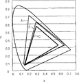
Fig. 6 is CIE (Commission Internationalede l ' Eclairage, the international lighting association) chromatic diagram that is used to explain color reprodubility.
Fig. 7 is the figure of the liquid crystal indicator of expression the 2nd embodiment of the present invention with the part of panel.
Fig. 8 is a liquid crystal indicator shown in Figure 7 enlarged drawing with the VIII-VIII line section of panel.
Fig. 9 is the figure that the variation 1 of the 2nd dyed layer is shown.
Figure 10 is the figure that the variation 2 of the 2nd dyed layer is shown.
Description of reference numerals
10: the 1 mother substrates; Zone, 12: the 1 unit (cell); 14: the 2 unit areas; 16: the 1 dyed layers; 18: the 1 colorant portions; 20: the 2 colorant portions; 22: the 3 colorant portions; 24: the 2 dyed layers; 25: the hole; 28: the 1 holes; 30: the 2 holes; 32: the 3 holes; 34: the 2 mother substrates; 36: liquid crystal; 38: the 1 alignment films; 40: the 2 alignment films; 42: overcoat; 44: black matrix; 124: the 2 dyed layers; 126: the hole; 146: cut zone; 148: jut; 210: the 1 mother substrates; 224: the 2 dyed layers; 226: the hole; 242: overcoat; 250: the translucent material layer; 310: the 1 mother substrates; 324: the 2 dyed layers; 326: the hole; 342: overcoat; 410: the 1 mother substrates; 424: the 2 dyed layers; 426: the hole; 442: overcoat.
Embodiment
Below, with reference to description of drawings embodiment of the present invention.
[the 1st embodiment]
Fig. 1 illustrates the skeleton diagram of the liquid crystal indicator of the 1st embodiment of the present invention with panel.Fig. 2 is a liquid crystal indicator shown in Figure 1 part enlarged drawing with the II-II line section of panel.Fig. 3 is a liquid crystal indicator shown in Figure 1 part enlarged drawing with the III-III line section of panel.Liquid crystal indicator is the goods that are used to cut out a plurality of display panels with panel.
Liquid crystal indicator for example comprises the 1st mother substrate 10 that is made up of glass with panel.The 1st mother substrate 10 is the parts that are used to cut out a plurality of filter substrates.As shown in Figure 1, the 1st mother substrate 10 comprises corresponding with a plurality of Unit the 1st (each display panels) respectively a plurality of the 1st unit areas 12 and corresponding with a plurality of Unit the 2nd (each display panels) respectively a plurality of the 2nd unit areas 14.14 to the 1 unit areas 12, the 2nd unit area are little.That is, liquid crystal indicator becomes with panel and can cut out a plurality of large-scale display panels corresponding with a plurality of Unit the 1st and a plurality of small-sized display panels corresponding with a plurality of Unit the 2nd.As variation, the 1st unit area 12 and the 2nd unit area 14 can be same sizes.
As shown in Figure 2, the 1st unit area 12 disposes the 1st dyed layer 16.The 1st dyed layer 16 comprises the 18, the 2nd colorant portion 20 of the 1st colorant portion and the 3rd colorant portion 22 that is made up of different colours, constitutes color filter.Fig. 4 is the vertical view that the part of the 1st dyed layer 15 is shown.
As shown in Figure 3, the 2nd unit area 14 disposes the 2nd dyed layer 24.The 2nd dyed layer 24 comprises the 18, the 2nd colorant portion 20 of the 1st colorant portion and the 3rd colorant portion 22 that is made up of different colours, constitutes color filter.Fig. 5 is the vertical view that the 2nd dyed layer 24 parts are shown.
The 1st dyed layer 16 and the 2nd dyed layer 24 are made up of identical materials respectively, have the identical part of thickness.For example, under the situation of using the pigment dispersing method, utilize to make the resin precursor of pigment dispersing form the 1st dyed layer 16 and the 2nd dyed layer 24.Particularly, form the 1st colorant portion 18 of the 1st dyed layer 16 and the 1st colorant portion 18 of the 2nd dyed layer 24 simultaneously.Form the 2nd colorant portion 20 of the 1st dyed layer 16 and the 2nd colorant portion 20 of the 2nd dyed layer 24 simultaneously.Form the 3rd colorant portion 22 of the 1st dyed layer 16 and the 3rd colorant portion 22 of the 2nd dyed layer 24 simultaneously.
For resin precursor, use mould to be coated with machine (die coater) or spin coater (spin coater) etc., can make by 1 technology forms layer thickness even.And carry out resin curing process or use under the situation of photoetching make public, video picture and baking technologies such as (bake).
In this embodiment, the 1st dyed layer 16 and the 2nd dyed layer 25 are made up of the layer of same material, same thickness, but constitute as the color reprodubility of color filter different.In order to realize this goal, the 1st dyed layer 16 does not have hole (with reference to Fig. 4), but on the 2nd dyed layer 24 in order to make color reprodubility lower and form hole (hole) 26 (with reference to Fig. 5) than the 1st dyed layer 16.Use photoetching and just can form hole 26 simply.
The hole 26 of the 2nd dyed layer 24 comprise the 1st colorant portion 18 that is formed on the 1st hole 28, be formed on the 2nd colorant portion 20 the 2nd hole 30, be formed on the 3rd hole 32 of the 3rd colorant portion 22.Opening through independent adjustment the 1st hole 28 can access desired color reprodubility at the opening in ratio shared in the 1st colorant portion 18, the 2nd hole 30 opening shared ratio in the 3rd colorant portion 22 in ratio shared in the 2nd colorant portion 20, the 3rd hole 32.If the ratio of opening is different, then color reprodubility is different.
Fig. 6 is CIE (Commission Internationalede l ' Eclairage, the international lighting association) chromatic diagram that is used to explain color reprodubility.Among Fig. 6, horseshoe-shaped part is represented human viewing area.Triangle A representes the scope of the color rendering of NTSC (National Television StandardsCommittee, National Television System Committee) specification.The triangle B that it is inboard, expression does not form the color rendering territory of the dyed layer in hole, and for example, NTSC is than the example that is 75%.Form hole and NTSC and represent by triangle C than the color rendering zone that is 55% dyed layer.
According to this embodiment, the 1st dyed layer 16 and the 2nd dyed layer 24, in the hole 26 supreme difference arranged, but have the identical part of thickness, thus only on the photomask of exposure manufacturing hole form the operation before pattern just can proceed to hole 26 formation simultaneously.Therefore, can easily form the different color filter of color reprodubility by a substrate.
Like Fig. 2 or shown in Figure 3, liquid crystal indicator comprises with panel and is used to cut out the 2nd mother substrate 34 a plurality of array base paltes, that for example be made up of glass.The 2nd mother substrate 34 comprises TFT, pixel electrode and distribution etc., also can be called the TFT substrate.Liquid crystal indicator can be IPS (In Plane Switching with the type of drive of panel; Dull and stereotyped switch) mode, TN (Twisted Nematic; Twisted-nematic) mode or VA (VerticalAlignment; Homeotropic alignment) any-mode of mode etc., and form electrode and distribution corresponding to mode.
Like Fig. 2 or shown in Figure 3, between a pair of substrate (the 1st mother substrate 10 and the 2nd mother substrate 34), clip liquid crystal (liquid crystal layer) 36.In detail, between the 2nd alignment films 40 of pasting on the 1st alignment films 38 of pasting on the 1st mother substrate 10 and the 2nd mother substrate 34, dispose liquid crystal 36.On the color-filter layer of being located at the 1st mother substrate 10 (the 1st dyed layer 16 and the 2nd dyed layer 24), be formed with overcoat 42.Configuration overcoat 42 makes it to contact with the inner face in hole 26.Corresponding to hole 26, also form depression on the surface of overcoat 42.In addition, via hole 26, overcoat 42 contacts with the 1st mother substrate 10.In addition, can omit overcoat 42 as required.On overcoat 42, dispose the 1st alignment film 38.Between the 1st mother substrate 10 and the 1st dyed layer 16 and the 2nd dyed layer 24, dispose black matrix 44.
Thereafter, the liquid crystal indicator of this embodiment is cut out a plurality of display panels with panel.Particularly, can obtain a plurality of large-scale display panels and a plurality of small-sized display panels.And can obtain same size but the different display panels of color rendering.
[the 2nd embodiment]
Fig. 7 is the figure of the liquid crystal indicator of expression the 2nd embodiment of the present invention with the part of panel.Fig. 8 is a liquid crystal indicator shown in Figure 7 enlarged drawing with the VIII-VIII line section of panel.
In this embodiment, be used to multiple domain (Multi-Domain) mode that the visual angle is enlarged.In the multiple domain mode, at 1 pixel internal storage in the different plural zone of the state of orientation of liquid crystal molecule.The 2nd dyed layer 124 comprises a plurality of cut zone 146 corresponding to the multiple domain mode.Through jut 148, mark off the different a plurality of cut zone 146 of state of orientation.These structures are also corresponding to the 1st not shown dyed layer.
In order to have eliminated the heterochromia that the visual angle causes, on each in a plurality of cut zone 146 of the 2nd dyed layer 124, make aperture area be identically formed hole 126.Other structure is corresponding to the content of explaining in the 1st embodiment.
[variation]
Fig. 9 is the figure that the variation 1 of the 2nd dyed layer is shown.In this example, the inside in the hole that is formed at the 2nd dyed layer 224 226 forms the colourless translucent material layer 250 that for example is made up of resin.Overcoat 242 is formed on the 2nd dyed layer 224 and the translucent material layer 250.In addition, can omit overcoat 242 as required.The content of explaining in the corresponding above-mentioned embodiment of other structures.
Figure 10 is the figure that the variation 2 of the 2nd dyed layer is shown.In this example, the hole 426 that is formed on the 2nd dyed layer 424 is the depressions that do not connect.In this example, also disposing overcoat 442 contacts with the inner face in hole 426.The part of overcoat 442 inserts 426.Corresponding to hole 426, the surface of overcoat 442 also forms depression.In addition, can also omit overcoat 442 as required.The content of explaining in the corresponding above-mentioned embodiment of other structures.
The invention is not restricted to above-mentioned embodiment and various distortion can be arranged.For example, the structure of in embodiment, explaining, the structure that can maybe can reach purpose equally with the structure of the same in fact structure, realization action effect is equally replaced.