CN101893955B - Display device and electronic unit - Google Patents
Display device and electronic unit Download PDFInfo
- Publication number
- CN101893955B CN101893955B CN2010101779861A CN201010177986A CN101893955B CN 101893955 B CN101893955 B CN 101893955B CN 2010101779861 A CN2010101779861 A CN 2010101779861A CN 201010177986 A CN201010177986 A CN 201010177986A CN 101893955 B CN101893955 B CN 101893955B
- Authority
- CN
- China
- Prior art keywords
- electrode
- phase
- display device
- detection signal
- noise
- Prior art date
- Legal status (The legal status is an assumption and is not a legal conclusion. Google has not performed a legal analysis and makes no representation as to the accuracy of the status listed.)
- Expired - Fee Related
Links
Images


Classifications
-
- G—PHYSICS
- G06—COMPUTING; CALCULATING OR COUNTING
- G06F—ELECTRIC DIGITAL DATA PROCESSING
- G06F3/00—Input arrangements for transferring data to be processed into a form capable of being handled by the computer; Output arrangements for transferring data from processing unit to output unit, e.g. interface arrangements
- G06F3/01—Input arrangements or combined input and output arrangements for interaction between user and computer
- G06F3/03—Arrangements for converting the position or the displacement of a member into a coded form
- G06F3/041—Digitisers, e.g. for touch screens or touch pads, characterised by the transducing means
- G06F3/044—Digitisers, e.g. for touch screens or touch pads, characterised by the transducing means by capacitive means
- G06F3/0445—Digitisers, e.g. for touch screens or touch pads, characterised by the transducing means by capacitive means using two or more layers of sensing electrodes, e.g. using two layers of electrodes separated by a dielectric layer
-
- G—PHYSICS
- G02—OPTICS
- G02F—OPTICAL DEVICES OR ARRANGEMENTS FOR THE CONTROL OF LIGHT BY MODIFICATION OF THE OPTICAL PROPERTIES OF THE MEDIA OF THE ELEMENTS INVOLVED THEREIN; NON-LINEAR OPTICS; FREQUENCY-CHANGING OF LIGHT; OPTICAL LOGIC ELEMENTS; OPTICAL ANALOGUE/DIGITAL CONVERTERS
- G02F1/00—Devices or arrangements for the control of the intensity, colour, phase, polarisation or direction of light arriving from an independent light source, e.g. switching, gating or modulating; Non-linear optics
- G02F1/01—Devices or arrangements for the control of the intensity, colour, phase, polarisation or direction of light arriving from an independent light source, e.g. switching, gating or modulating; Non-linear optics for the control of the intensity, phase, polarisation or colour
- G02F1/13—Devices or arrangements for the control of the intensity, colour, phase, polarisation or direction of light arriving from an independent light source, e.g. switching, gating or modulating; Non-linear optics for the control of the intensity, phase, polarisation or colour based on liquid crystals, e.g. single liquid crystal display cells
- G02F1/133—Constructional arrangements; Operation of liquid crystal cells; Circuit arrangements
- G02F1/1333—Constructional arrangements; Manufacturing methods
- G02F1/13338—Input devices, e.g. touch panels
-
- G—PHYSICS
- G06—COMPUTING; CALCULATING OR COUNTING
- G06F—ELECTRIC DIGITAL DATA PROCESSING
- G06F3/00—Input arrangements for transferring data to be processed into a form capable of being handled by the computer; Output arrangements for transferring data from processing unit to output unit, e.g. interface arrangements
- G06F3/01—Input arrangements or combined input and output arrangements for interaction between user and computer
- G06F3/03—Arrangements for converting the position or the displacement of a member into a coded form
- G06F3/041—Digitisers, e.g. for touch screens or touch pads, characterised by the transducing means
- G06F3/0412—Digitisers structurally integrated in a display
-
- G—PHYSICS
- G06—COMPUTING; CALCULATING OR COUNTING
- G06F—ELECTRIC DIGITAL DATA PROCESSING
- G06F3/00—Input arrangements for transferring data to be processed into a form capable of being handled by the computer; Output arrangements for transferring data from processing unit to output unit, e.g. interface arrangements
- G06F3/01—Input arrangements or combined input and output arrangements for interaction between user and computer
- G06F3/03—Arrangements for converting the position or the displacement of a member into a coded form
- G06F3/041—Digitisers, e.g. for touch screens or touch pads, characterised by the transducing means
- G06F3/044—Digitisers, e.g. for touch screens or touch pads, characterised by the transducing means by capacitive means
- G06F3/0446—Digitisers, e.g. for touch screens or touch pads, characterised by the transducing means by capacitive means using a grid-like structure of electrodes in at least two directions, e.g. using row and column electrodes
-
- G—PHYSICS
- G06—COMPUTING; CALCULATING OR COUNTING
- G06F—ELECTRIC DIGITAL DATA PROCESSING
- G06F3/00—Input arrangements for transferring data to be processed into a form capable of being handled by the computer; Output arrangements for transferring data from processing unit to output unit, e.g. interface arrangements
- G06F3/01—Input arrangements or combined input and output arrangements for interaction between user and computer
- G06F3/03—Arrangements for converting the position or the displacement of a member into a coded form
- G06F3/041—Digitisers, e.g. for touch screens or touch pads, characterised by the transducing means
- G06F3/044—Digitisers, e.g. for touch screens or touch pads, characterised by the transducing means by capacitive means
- G06F3/0448—Details of the electrode shape, e.g. for enhancing the detection of touches, for generating specific electric field shapes, for enhancing display quality
-
- G—PHYSICS
- G09—EDUCATION; CRYPTOGRAPHY; DISPLAY; ADVERTISING; SEALS
- G09G—ARRANGEMENTS OR CIRCUITS FOR CONTROL OF INDICATING DEVICES USING STATIC MEANS TO PRESENT VARIABLE INFORMATION
- G09G3/00—Control arrangements or circuits, of interest only in connection with visual indicators other than cathode-ray tubes
- G09G3/20—Control arrangements or circuits, of interest only in connection with visual indicators other than cathode-ray tubes for presentation of an assembly of a number of characters, e.g. a page, by composing the assembly by combination of individual elements arranged in a matrix no fixed position being assigned to or needed to be assigned to the individual characters or partial characters
- G09G3/34—Control arrangements or circuits, of interest only in connection with visual indicators other than cathode-ray tubes for presentation of an assembly of a number of characters, e.g. a page, by composing the assembly by combination of individual elements arranged in a matrix no fixed position being assigned to or needed to be assigned to the individual characters or partial characters by control of light from an independent source
- G09G3/36—Control arrangements or circuits, of interest only in connection with visual indicators other than cathode-ray tubes for presentation of an assembly of a number of characters, e.g. a page, by composing the assembly by combination of individual elements arranged in a matrix no fixed position being assigned to or needed to be assigned to the individual characters or partial characters by control of light from an independent source using liquid crystals
- G09G3/3611—Control of matrices with row and column drivers
- G09G3/3614—Control of polarity reversal in general
-
- G—PHYSICS
- G06—COMPUTING; CALCULATING OR COUNTING
- G06F—ELECTRIC DIGITAL DATA PROCESSING
- G06F2203/00—Indexing scheme relating to G06F3/00 - G06F3/048
- G06F2203/041—Indexing scheme relating to G06F3/041 - G06F3/045
- G06F2203/04107—Shielding in digitiser, i.e. guard or shielding arrangements, mostly for capacitive touchscreens, e.g. driven shields, driven grounds
-
- G—PHYSICS
- G09—EDUCATION; CRYPTOGRAPHY; DISPLAY; ADVERTISING; SEALS
- G09G—ARRANGEMENTS OR CIRCUITS FOR CONTROL OF INDICATING DEVICES USING STATIC MEANS TO PRESENT VARIABLE INFORMATION
- G09G3/00—Control arrangements or circuits, of interest only in connection with visual indicators other than cathode-ray tubes
- G09G3/20—Control arrangements or circuits, of interest only in connection with visual indicators other than cathode-ray tubes for presentation of an assembly of a number of characters, e.g. a page, by composing the assembly by combination of individual elements arranged in a matrix no fixed position being assigned to or needed to be assigned to the individual characters or partial characters
- G09G3/34—Control arrangements or circuits, of interest only in connection with visual indicators other than cathode-ray tubes for presentation of an assembly of a number of characters, e.g. a page, by composing the assembly by combination of individual elements arranged in a matrix no fixed position being assigned to or needed to be assigned to the individual characters or partial characters by control of light from an independent source
- G09G3/36—Control arrangements or circuits, of interest only in connection with visual indicators other than cathode-ray tubes for presentation of an assembly of a number of characters, e.g. a page, by composing the assembly by combination of individual elements arranged in a matrix no fixed position being assigned to or needed to be assigned to the individual characters or partial characters by control of light from an independent source using liquid crystals
- G09G3/3611—Control of matrices with row and column drivers
- G09G3/3648—Control of matrices with row and column drivers using an active matrix
Abstract
The display device with high detection accuracy includes: display pixel electrodes; a common electrode; a display function layer; a display control circuit performing image display control by applying a pixel voltage to each of the display pixel electrodes and applying a common drive voltage to the common electrode, the common drive voltage inverting in synchronization with a drive cycle of the image display control; a touch detection electrode cooperating with the common electrode to form a capacitor; and a touch detection circuit detecting an external proximity object, based on a detection signal obtained from the touch detection electrode in response to the common drive voltage applied to the common electrode. The touch detection circuit performs the detection operation in a inversion period following an inversion timing of the common drive voltage, based on both first and second detection signals obtained before and after the inversion timing, respectively.
Description
Technical field
The present invention relates to a kind of display device such as liquid crystal display, more particularly, the present invention relates to a kind of display device that comprises capacitive touch sensor, and the touch of finger by the user etc., information can be input in the described display device, the invention still further relates to the electronic unit with such display device.
Background technology
In recent years, paid close attention to such display unit, the contact detecting device (hereinafter referred to as touch sensor) that wherein is commonly referred to touch panel is directly installed on the liquid crystal display and makes this liquid crystal display show that various buttons are used for input message rather than the typical button of setting (provide).In the trend that screen size increases on mobile device, this technology is brought the huge advantage such as space saving and part count minimizing so that the common arrangement of display and button becomes possibility.Yet this technology has following problem, increases such as the thickness owing to installation touch sensor thereby whole Liquid Crystal Module.Particularly, when this technology is applied to mobile device, protective seam need to be set preventing the scuffing on the touch panel, thereby, following problem is arranged, namely the thickness of Liquid Crystal Module trend increases, and runs counter to the trend that thickness reduces.
Each proposes a kind of liquid crystal display cells with capacity type touch panel that thickness reduces the open No.2008-9750 of Japanese unexamined patent and U.S. Patent No. 6057903.In this type, the conducting film of touch panel be arranged on be positioned at liquid crystal display cells watch on the side substrate and in being used between the polaroid (polarizing plate) of watching that the outside surface of watching the substrate on the side is settled, and the capacity type touch panel is formed between the outside surface of the conducting film of touch panel and polaroid, so that the outside surface of this polaroid is as touch-surface.
Summary of the invention
Yet, in each of the open No.2008-9750 of Japanese unexamined patent and U.S. Patent No. 6057903 in the disclosed liquid crystal display cells with touch panel, need in theory for the conducting film of touch panel having the electromotive force identical with user's electromotive force, and need the suitable ground connection of user.Therefore, be difficult in the practice liquid crystal display cells with touch panel is applied to mobile device by the static television receiver from the external power source of socket etc. unlike being applied to.And, in above-mentioned technology, need to allow for the conducting film of touch panel very near user's finger, therefore, arrange to be used for conducting film regional restricted of touch panel, for example, to be difficult in the part of for example liquid crystal display cells deep inside, arrange the conducting film for touch panel.In other words, design flexibility is low.And, in above-mentioned technology, need to arrange display driver circuit part with liquid crystal display cells in the configuration mutually independently such as the circuit part of touch panel drive part and coordinate measurement part, cause to be difficult to the circuit of equipment is integrated into an integral body.
Can conceive, can newly arrange and touch detecting electrode so that capacitor is formed between touch detecting electrode and the public electrode, public electrode is provided for applying the driving voltage (display device provides the touch sensor of the capacity type with new configuration) for display originally.This capacitor exists or does not exist according to the touch of object and changes.Therefore, when the driving voltage that be used for to show that is applied to public electrode by display control circuit during also with the driving signal that is used for as touch sensor, depend on that the detection signal of the change of capacitor obtains from touching detecting electrode.When this detection signal was input in the predetermined touch testing circuit, touch that can detected object existed and does not still exist.And, according to this technology, the display device with the touch sensor that is suitable for being applied to the frequent unsettled mobile device of user's electromotive force can be obtained, and the display device of the touch sensor that designs in the mode of high flexible with the type of with good grounds Presentation Function layer can be obtained.And this technology provides such advantage, and the circuit that be used for to show and the circuit that is used for sensor are integrated in single circuit board simply, make circuit integrated easily.
Yet, band just like as described in the open No.2008-9750 of Japanese unexamined patent and the U.S. Patent No. 6057903, and display device according to the capacity type touch sensor of above-mentioned new configuration in, there is such problem, when picture element signal (picture signal) was written in the display element of each pixel, the noise that is derived from this write operation added detection signal to.
Therefore, in U.S. Patent No. 6057903, transparency conducting layer (screen layer) is arranged between touch panel and the display element, so that the fault that prevents from being caused by the noise that the picture signal write operation causes (detecting wrong).By conductive layer is maintained fixed potential, can shield the noise from display element.
Yet, in this technology, because large electric capacity is formed between signal lines and the screen layer, therefore there is such problem, the large degree of detection signal that obtains from signal lines dies down, and perhaps the large degree of the electric capacity of drive wire increases, so that power consumption etc. increases to a great extent.
Simultaneously, in the display device that provides the capacity type touch sensor with new configuration, because by in display panel, coming the detection position with writing waveform, so can conceive and to be difficult to remove or eliminate the noise that is derived from the picture signal write operation by screen layer is set in the effective display area territory.
As mentioned above, in the display device with the capacity type touch sensor in past, be difficult to be derived from the noise of picture signal write operation by elimination and do not improve the degree of accuracy of detected object with screen layer.
In view of aforementioned, be desirable to provide the display device that comprises the capacity type touch sensor, it can improve the degree of accuracy of detected object and need not to use screen layer, it would also be desirable to provide the electronic unit with such display device.
According to the embodiment of the invention, a kind of display device is provided, comprising: a plurality of display pixel electrodes; Public electrode is towards the display pixel electrode; The Presentation Function layer has image display function; Display control circuit comes carries out image to show control by applying pixel voltage to each display pixel electrode and applying common driver voltage to public electrode, and common driver voltage and image show that the drive cycle of control is synchronously anti-phase; Touch detecting electrode, cooperate to form capacitor with public electrode; And touch detection circuit, based on the detection signal that obtains from touching detecting electrode in response to the common driver voltage that is applied to public electrode, carry out the detection operation that detects near outside object, wherein, based on the second detection signal that obtains at the first detection signal that obtains before the anti-phase timing with after anti-phase timing the two, touch detection circuit is carried out detection and is operated in the anti-phase period the anti-phase timing of common driver voltage after.
Comprise display device with touch sensor according to the electronic unit of the embodiment of the invention.Display device comprises: a plurality of display pixel electrodes; Public electrode is towards the display pixel electrode; The Presentation Function layer has image display function; Display control circuit comes carries out image to show control by applying pixel voltage to each display pixel electrode and applying common driver voltage to public electrode, and common driver voltage and image show that the drive cycle of control is synchronously anti-phase; Touch detecting electrode, cooperate to form capacitor with public electrode; And touch detection circuit, based on the detection signal that obtains from touching detecting electrode in response to the common driver voltage that is applied to public electrode, carry out the detection operation that detects near outside object, wherein, based on the second detection signal that obtains at the first detection signal that obtains before the anti-phase timing with after anti-phase timing the two, touch detection circuit is carried out detection and is operated in the anti-phase period the anti-phase timing of common driver voltage after.
In these display devices and electronic unit, capacitor is formed between the touch detecting electrode that is provided to apply the public electrode of common driver voltage originally and newly provides.This capacitor depends on that the touch of object exists or do not exist and changes.Therefore, by the common driver voltage that is applied to public electrode by display control circuit is also driven signal as touch sensor, depend on the detection signal of the change of capacitor from touching the detecting electrode acquisition.By the detection signal that obtains is input in the touch detection circuit, the position that object touches (touch such as object exists or non-existent factor) is detected.At this, based on the second detection signal that obtains at the first detection signal that obtains before the anti-phase timing with after anti-phase timing the two, touch detection circuit is synchronously carried out to detect in the anti-phase period after the anti-phase timing of anti-phase common driver voltage at the drive cycle that shows control with image and is operated.Thus, the result who shows control period carries out image signal writing operation as image before anti-phase, in the impact of the noise (anti-phase rear noise) that can in the detection signal of eliminating after anti-phase, comprise, carry out detection in the anti-phase period anti-phase after and operate.
According to these display devices and electronic unit, based on the detection signal that obtains from touching detecting electrode according to the change of capacitor, the touch location of detected object, and based on the second detection signal that obtains at the first detection signal that obtains before the anti-phase timing with after anti-phase timing the two, touch detection circuit is carried out detection and is operated in the anti-phase period the anti-phase timing of common driver voltage after.Correspondingly, can in the impact of eliminating anti-phase rear noise, carry out in the anti-phase period after anti-phase and detect operation, and need not to use existing screen layer.Thereby, can improve the degree of accuracy of object detection in the display device with capacity type touch sensor, and need not to use screen layer.
Description of drawings
Figure 1A and Figure 1B explain with the principle of operation of the display device of the touch sensor of the with good grounds embodiment of the invention and illustrate to point the not figure of contact condition.
Fig. 2 A and Fig. 2 B explain with the principle of operation of the display device of the touch sensor of the with good grounds embodiment of the invention and the figure of finger contact state are shown.
Fig. 3 explains with the principle of operation of the display device of the touch sensor of the with good grounds embodiment of the invention and the example of drive signal waveform is shown and the figure of the example of the detection signal waveform of touch sensor.
Fig. 4 is the sectional view of configuration of the display device of schematically illustrated touch sensor with good grounds first embodiment of the invention.
Fig. 5 is the stereographic map of the configuration example of major part that the display device shown in Fig. 4 is shown (public electrode and be used for the detecting electrode of sensor).
Fig. 6 is the circuit diagram that the configuration example of testing circuit in the display device shown in Fig. 4 etc. is shown.
Fig. 7 is the synoptic diagram of example that the operation of the line order that drives public electrode is shown.
Fig. 8 is the timing waveform of the noise of explaining that the picture signal write operation of execution when operate by the detection in display device causes.
Fig. 9 is the timing waveform of explaining detection signal waveform and detecting the relation between the period.
Figure 10 be illustrated in common drive signal anti-phase before and afterwards the detection signal waveform of time in writing in vain (whitewriting) and black each the timing waveform of example that writes detection signal waveform in (black writing).
Figure 11 be illustrated in common drive signal anti-phase before and afterwards time in the detection signal waveform that comprises noise with eliminate each the timing waveform of example of noise detection signal waveform subsequently.
Figure 12 illustrates the process flow diagram that detects the example of operation in the testing circuit shown in Figure 6.
Figure 13 illustrates the process flow diagram that detects another example of operation in the testing circuit shown in Figure 6.
Figure 14 illustrates the process flow diagram that detects the another example of operation in the testing circuit shown in Figure 6.
Figure 15 be indication according to detection method change write in vain in detected signal value and the table of the example of the difference between the detected signal value in black the writing.
Figure 16 is the sectional view of configuration of the display device of schematically illustrated touch sensor with good grounds second embodiment of the invention.
Figure 17 A and Figure 17 B are respectively sectional view and the planimetric maps that the details in the configuration of pixel base part in the display device shown in Figure 16 is shown.
Figure 18 A and Figure 18 B are the amplification stereograms of the major part of display device shown in Figure 16.
Figure 19 A and Figure 19 B are the sectional views of explaining the operation of display device shown in Figure 16.
Figure 20 is the sectional view of configuration of display device of the touch sensor of schematically illustrated variant with good grounds the second embodiment.
Figure 21 is the sectional view of configuration of display device of the touch sensor of schematically illustrated another variant with good grounds the second embodiment.
Figure 22 is the stereographic map that the configuration of major part with the display device of the touch sensor of with good grounds variant 1 of the present invention (public electrode and be used for the detecting electrode of sensor) is shown.
Figure 23 is the stereographic map that the configuration of major part with the display device of the touch sensor of with good grounds variant 2 of the present invention (public electrode and be used for the detecting electrode of sensor) is shown.
Figure 24 is according to the three-dimensional external view of the display device of example application 1 of above-described embodiment and so on when observing from the front.
Figure 25 A and Figure 25 B are respectively the three-dimensional external views of observing the display device of example application 2 according to above-described embodiment and so on when from the front and back.
Figure 26 is the three-dimensional external view of example application 3.
Figure 27 is the three-dimensional external view of example application 4.
Figure 28 A to Figure 28 G be respectively that front elevation, side view, the front elevation of closed condition, the left side of example application 5 attempted, right side view, top view, and backplan.
Embodiment
Describe hereinafter with reference to the accompanying drawings the embodiment of the invention in detail.Incidentally, description will provide in the following order.
The ultimate principle of touch detecting system
1. the first embodiment (using the example of the anti-phase rear object detection of the detected value of Vcom before anti-phase)
2. the second embodiment (the liquid crystal cell of side electric field patterns as the example of display element)
3. variant (variant 1 and 2: have public electrode and be used for the example of other configuration of the detecting electrode of sensor)
4. example application (will be applied to the display device of touch sensor the example of electronic unit)
[ultimate principle of touch detecting system]
At first, with reference to Figure 1A to Fig. 3, with the ultimate principle of description with the touch detecting system in the display device of the touch sensor of with good grounds embodiment.This touch detecting system is embodied as the capacity type touch sensor.For example, shown in Figure 1A, the pair of electrodes (drive electrode E1 and detecting electrode E2) that is arranged as mutually towards and wherein inserts dielectric D is used for configuration capacitor element C1.This system also illustrates as equivalent electrical circuit in Figure 1B.Capacitor element C1 disposes drive electrode E1, detecting electrode E2 and dielectric D.The end of capacitor element C1 is connected to AC signal source (source driving signal) S, and other end P is via resistor R ground connection, and is connected to voltage-level detector (testing circuit) DET.When preset frequency (for example, when AC square wave Sg about a few kHz to tens kHz) (part of Fig. 3 (B)) is applied to drive electrode E1 from AC signal source S (end of capacitor element C1), the output waveform shown in the part of Fig. 3 (A) (detection signal Vdet) appears at detecting electrode E2 (the described other end P of capacitor element C1).Incidentally, Sg is corresponding with common drive signal Vcom for this AC square wave, is described further below.
Pointing not under the touch condition, shown in Figure 1A and Figure 1B, when capacitor element C1 was carried out charge/discharge, electric current I 0 flowed according to the capacitance of capacitor element C1.At this moment, for example as the waveform V0 in the part (A) of Fig. 3, this is detected by voltage-level detector DET the waveform of the electromotive force of other end P described in the capacitor element C1.
On the other hand, under the finger touch state, shown in Fig. 2 A and Fig. 2 B, the capacitor element C2 that is formed by finger is concatenated into capacitor element C1.Under this state, when to capacitor element C1 and C2 execution charge/discharge, difference streaming current I1 and I2.At this moment, for example as the waveform V1 in the part (A) of Fig. 3, this is detected by voltage-level detector DET the waveform of the electromotive force of other end P described in the capacitor element C1.At this moment, the electromotive force at described other end P place is minute electromotive force that the value by the electric current I 1 of flow through respectively capacitor element C1 and C2 and I2 limits.Therefore, waveform V1 becomes the value less than the waveform V0 in the touch condition not.As will be described below, voltage-level detector DET compares the voltage that detects with predetermined threshold voltage Vth.When the voltage that detects was equal to or greater than threshold voltage vt h, voltage-level detector DET determined that it is in not touch condition.On the other hand, when the voltage that detects during less than threshold voltage vt h, this detecting device DET determines that it is in touch condition.In this way, can carry out touch detects.
[1. the first embodiment]
[configuration example of display device 1]
Fig. 4 illustrates the cross-sectional configurations figure with the major part of the display device 1 of the touch sensor of with good grounds first embodiment of the invention.In display device 1, used for liquid crystal display element is made display element, use the electrode part (public electrode 43 that is arranged in this liquid crystal display cells originally, will be described below) and be used for driving signal (the common drive signal Vcom of display, will be described below), dispose thus the capacity type touch sensor.
As shown in Figure 4, display device 1 comprises: pixel substrate 2; The relative substrate 4 of pixel-oriented substrate 2; And the liquid crystal layer 6 that between pixel substrate 2 and relative substrate 4, inserts.
Pixel substrate 2 comprises: TFT (thin film transistor (TFT)) substrate 21, as circuit substrate; And a plurality of pixel electrodes 22, with matrix arrangement in TFT substrate 21.Except unshowned each display driver and TFT for driving pixel electrode 22, also in TFT substrate 21, form such as supplying with the source electrode line of picture element signals to each pixel electrode 22 and driving the wire of the gate line of each TFT.And, in TFT substrate 21, can also form to carry out to touch and detect the testing circuit 8 (Fig. 6) that operates, will be described below.
Substrate 4 comprises relatively: substrate of glass 41; Be formed on a lip-deep color filters 42 of this substrate of glass 41; And be formed on public electrode 43 on this color filters 42.In this color filters 42, for example, the color filters layer of three colors red (R), green (G), blue (B) is arranged circularly, distributes three colors of one group of RGB (pixel electrode 22) to each display pixel.Public electrode 43 is also with the detecting electrode that acts on sensor, and the detecting electrode that should be used for sensor forms carries out a part that touches the touch sensor that detects operation, and this public electrode 43 is corresponding with the drive electrode E1 among Figure 1A.
On another surface of substrate of glass 41, be formed for the detecting electrode 44 (touch detecting electrode) of sensor.And, be used herein on the detecting electrode 44 of sensor, arrange polaroid 45.The detecting electrode 44 that is used for sensor forms the part of touch sensor, and corresponding with the detecting electrode E2 among Figure 1A.
Orientation (alignment) film is arranged in and reaches between liquid crystal layer 6 and the pixel substrate 2 between liquid crystal layer 6 and the relative substrate 4.Although the polaroid on the light incident side is arranged under the pixel substrate 2, its diagram is omitted in the drawings.
Fig. 5 is stereographic map, public electrode 43 in the relative substrate 4 is shown and is used for the configuration example of the detecting electrode 44 of sensor.In this example, public electrode 43 is divided into a plurality of strip electrode patterns (at this, take six public electrodes 431 to 436 as example) in the left and right directions extension of figure.In driver 43D, common drive signal Vcom is applied to each electrode pattern successively, and the line sequential scanning drives timesharing and carries out, such as hereinafter description.On the other hand, the detecting electrode 44 that is used for sensor is included in a plurality of strip electrode patterns that extend with the direction of the bearing of trend phase quadrature of public electrode 43 electrode patterns.Detection signal Vdet is from each electrode pattern output of the detecting electrode 44 that is used for sensor, and is input to testing circuit shown in Figure 68.
[example that comprises the Circnit Layout of source driving signal S and testing circuit 8]
Fig. 6 illustrates the example of the Circnit Layout of source driving signal S and the testing circuit 8 that comprises shown in Figure 1B and the sequential control part 9 that is used as the sequential maker.Capacitor element C11 to C16 shown in Figure 6 is respectively with public electrode 431 to 436 shown in Figure 5 with to be used for (static) capacitor element of forming between the detecting electrode 44 of sensor corresponding.
Source driving signal S for capacitor element C11 to C16 each and arrange, comprising: SW control section 11; Two switching devices 12 and 15; Two inverter circuits 131 and 132; Operational amplifier 14.Connection (on) and (off) state of cut-out of SW control section 11 control switching devices 12 are controlled the connection status between power supply+V and phase inverter 131 and 132 thus.The input terminal of inverter circuit 131 is connected to an end (terminal relative with power supply+V) of switching device 12 and the lead-out terminal of inverter circuit 132.The lead-out terminal of inverter circuit 131 is connected to the input terminal of inverter circuit 132 and the input terminal of operational amplifier 14.Thus, phase inverter 131 and 132 oscillatory circuits as output predetermined pulse signal.Operational amplifier 14 be connected to two power supply+V and-V.According to the timing control signal CTL1 that is supplied with by sequential control part 9, the connection (on) of control switching device 15 and (off) state of cut-out.Particularly, utilize switching device 15, an end of each of capacitor element C11 to C16 (in public electrode 431 to 436 sides) is connected to lead-out terminal or the ground connection of operational amplifier 14.Thus, common drive signal Vcom is supplied to capacitor element C11 to C16 from source driving signal S.
Testing circuit 8 (voltage-level detector DET) comprising: amplifier section 81; A/D (simulation is to numeral) conversion portion 83; Signal processing 84; Coordinate Extraction parts 85; Reach the resistor R that preamble is mentioned.Incidentally, the input terminal Tin of testing circuit 8 is connected to each (be used for detecting electrode 44 sides of sensor on) other end of capacitor element C11 to C16, shares with this other end.
Resistor R is arranged between the tie point P and ground on the side of the positive input terminal (+) that operational amplifier 811 is set.Resistor R is by avoiding keeping steady state (SS) for the floating of detecting electrode 44 of sensor.This provides following advantage, and namely in testing circuit 8, the unstable or fluctuation of the signal value of detection signal Vdet is avoided, and simultaneously, static is dissipated to ground via resistor R.
A/D conversion portion 83 is converted to digital detection signal to the detection signal Vdet that amplifies of analog form in amplifier section 81, comprise unshowned comparer.This comparer is relatively inputted the electromotive force of detection signal and the electromotive force (seeing Fig. 3) of predetermined threshold voltage Vth.Amplification when incidentally, the A/D in the A/D conversion portion 83 changes regularly is subjected to be controlled by the timing control signal CTL2 that sequential control part 9 is supplied with.
Whether coordinate Extraction parts 85 obtains testing result according to the detection signal (eliminating the detection signal of anti-phase rear noise) from signal processing 84 outputs (has touch, and output is from the testing result of lead-out terminal Tout and the coordinate that touch location when touching is arranged).
Incidentally, so the testing circuit 8 of configuration can be formed in the outer peripheral areas (non-display area or frame zone) in the relative substrate 4.Perhaps, testing circuit 8 can be formed in the outer peripheral areas in the pixel substrate 2.Yet when testing circuit 8 was formed in the pixel substrate 2, testing circuit 8 and the original various circuit components for showing control etc. that are formed in the pixel substrate 2 were integrated, and from by the integrated viewpoint that realizes circuit reduction, this is preferred.In the case, each electrode pattern of the detecting electrode 44 that is used for sensor in the pixel substrate 2 and testing circuit 8 be similar to the contact conductive pole (not shown) that contact conductive pole 7 and link to each other, detection signal Vdet can transfer to testing circuit 8 from the detecting electrode 44 for sensor.
[operation of display device 1 and effect]
Now, will operation and the effect of display device 1 be described.
(basic operation)
In display device 1, the display driver (not shown) of pixel substrate 2 is supplied with common drive signal Vcom with the line order to each electrode pattern (such as public electrode 431 to 436) in the public electrode 43.Display driver is also supplied with picture element signals (picture signal) via source electrode line to pixel electrode 22, and supplies with synchronously with this of picture element signal, by the switching of gate line with the TFT in each pixel electrode of line sequential control.Thus, electric field is being applied to the liquid crystal layer 6 of each pixel by common drive signal Vcom with the longitudinal direction (direction vertical with substrate) that each picture element signal limits, and modulates mesomorphic state.In this way, in so-called anti-phase driving, carry out demonstration.
On the other hand, in relative substrate 4 sides, capacitor element C1 (capacitor element C11 to C16) is formed on each electrode pattern in the public electrode 43 and is used for each cross part office of each electrode pattern of the detecting electrode 44 of sensor.At this, for example, such as the part (A) of Fig. 7 to shown in the part (C), when common drive signal Vcom timesharing is applied to each electrode pattern in the public electrode 43 successively, to the electrode pattern in the public electrode 43 that is applied in common drive signal Vcom be used for each of capacitor element C11 to C16 of the line that the cross part office of each electrode pattern of the detecting electrode 44 of sensor forms, carry out charge/discharge.The result is, has the detection signal Vdet of amplitude of the capacity that depends on capacitor element C1 from each electrode pattern output of the detecting electrode 44 that is used for sensor.Do not contact under the state on surface of relative substrate 4 the amplitude constant of this detection signal Vdet at user's finger.With the line of the capacitor element C1 that is recharged/discharges by utilizing common drive signal Vcom to scan with the line ordinal shift.
Incidentally, when each electrode pattern in the public electrode 43 drives with the line order as mentioned above, preferably, as shown in Figure 7, carry out the driving operation of line order by the part of the electrode pattern in the binding public electrode 43.More specifically, the drive wire L that disposes this part of electrode pattern comprises detection drive wire L1 and display driver line L2, detects the electrode pattern that drive wire L1 disposes a plurality of lines, and display driver line L2 is made of several lines (at this, a line) of electrode pattern.This is so that can suppress according to the shape of the electrode pattern in the public electrode 43 because the deterioration in image quality that the appearance of line and point causes.
At this, when lip-deep any position of user's the relative substrate 4 of finger touch, the capacitor element C2 that is formed by this finger is added into the capacitor element C1 that original position touching forms.The result is, the value of the detection signal Vdet of when electrode pattern corresponding with this touch location (, among common drive signal Vcom is applied to the electrode pattern of public electrode 43) becomes less than the detection signal Vdet of other position when scanning this touch location.Testing circuit 8 (Fig. 6) is this detection signal Vdet and threshold voltage vt h relatively.As detection signal Vdet during less than threshold voltage vt h, testing circuit 8 is institute's touch location with this location positioning.This touch location can and detect less than the timing of the detection signal Vdet of threshold voltage vt h based on the timing that applies common drive signal Vcom to be determined.
In this way, in the display device 1 with the touch sensor of with good grounds present embodiment, original public electrode that provides in liquid crystal display cells 43 is also as one of paired electrode (drive electrode and detecting electrode) of touch sensor.In addition, also be used as the driving signal of touch sensor as the common drive signal Vcom of display drive signals.Thus, in the capacity type touch sensor, the detecting electrode 44 that only is used for sensor provides as newly-installed electrode, and does not need newly to be provided for the driving signal of touch sensor.Therefore, configuration is simple.
And, in the display device (the open No.2008-9750 of Japanese unexamined patent) with the touch panel of correlation technique, the current amplitude of sensor of flowing through is accurately measured, and based on this measured value, determines institute's touch location by analog computation.On the other hand, in the display device 1 according to present embodiment, digitally detect the existence of the existence depend on touch or the relative changes in the non-existent electric current (change of electromotive force) or do not exist, thus, can improve with the testing circuit of easy configuration the detection degree of accuracy.And, being provided for the public electrode 43 that applies common drive signal Vcom and being used for of newly providing forms capacitor between the detecting electrode 44 of sensor original, the change that is derived from this capacitor of user's finger touch by utilization is carried out to touch and is detected.Thus, the display device with the touch panel of present embodiment can be applied to the frequent unsettled mobile device of user's electromotive force.
And, be divided into a plurality of electrode patterns owing to be used for the detecting electrode 44 of sensor, and each the respectively timesharing driving in a plurality of electrode pattern, therefore, the position that touches can detect.
(the operation of characteristic; Use the detection operation of noise Processing for removing)
Below, with reference to Fig. 8 to Figure 15, will describe the detection operation of the use noise Processing for removing of one of feature as present embodiment in detail.
At first, shown in the part (A) of Fig. 8, when common drive signal Vcom with such as the part (B) of Fig. 8 and the drive cycle (the 1H period of picture signal) of the image (C) demonstration control period use synchronously stand when anti-phase, obtain the detection waveform of the detection signal Vdet as shown in the part (D) to (F) such as Fig. 8.In other words, detection signal Vdet and above-mentioned anti-phase synchronously anti-phase owing to flow into the leakage current of above-mentioned resistor R, weakens gradually at anti-phase afterwards signal value.Incidentally, for convenience, suppose that the impact of anti-phase rear noise is removed or eliminates, the detection waveform among Fig. 8 (partly (D) is to (F)) is shown.
At this moment, when carry out as the part (B) of Fig. 8 and partly shown in (C) such as writing in vain and deceiving the picture element signal (picture signal) that writes and write fashionable, as shown in the part (E) and part (F) of for example Fig. 8, be derived from this noise that writes and be included in the detection waveform of detection signal Vdet.Particularly, the 1H period comprises and non-ly writes period Δ tA and write period Δ tB, does not apply picture signal non-during writing period Δ tA, and during writing period Δ tB, apply picture signal, according to the tone level of picture element signal, during writing period Δ tB, the change of detection waveform occurs.In other words, the tone level of (after anti-phase) picture signal according at that time, shown in the part (E) and the arrow in the part (F) of Fig. 8, the anti-phase rear noise that anti-phase rear picture signal causes is included in the detection waveform of detection signal Vdet.More specifically, write the fashionable anti-phase rear noise that comprises with common drive signal Vcom homophase black, and writing in vain the fashionable anti-phase rear noise anti-phase with common drive signal Vcom that comprise.In this way, during writing period Δ tB, because anti-phase rear noise, the detection waveform of detection signal Vdet changes according to the tone level of picture element signal, thus, the change (part of Fig. 3 (A)) in the detection waveform that is difficult to such change and the existence that touches such as object or non-existent factor are caused distinguishes.
Simultaneously, for example, as shown in Figure 9, corresponding with at once time after common drive signal Vcom is anti-phase non-write period Δ tA during, comparing greatly in touching the voltage change amount that causes owing to object and writing period Δ tB.Therefore, the composition of the change from remove the detection waveform that is caused by the existence that touches such as object or non-existent factor and the isolated angle of this composition and noise Processing for removing, preferably, after this is anti-phase, A/D conversion portion 83 in the testing circuit 8 obtains anti-phase detection signal before immediately, will describe in detail later.And, consider the detection sensitivity of the existence that touches such as object or non-existent factor high, and the impact of the anti-phase rear noise that is described further below is little, and the time (the non-period Δ tA that writes) before the picture signal write operation that the anti-phase detection afterwards that hope is described further below operates in this anti-phase rear execution begins carries out.
At this, in fact, as shown in figure 10, noise (that is, the anti-phase front noise that the picture signal that comprises in the anti-phase detection signal before causes; Corresponding with the electric potential difference Δ VB among the figure) non-in the detection signal after also causing (resultas) anti-phase write the anti-phase rear noise during the period Δ tA.In other words, according to the amplitude of the electric potential difference Δ VB corresponding with anti-phase front noise (that is, according to the electromotive force of the tone level of anti-phase preceding pixel signal), limit the amplitude of the electric potential difference Δ VA corresponding with anti-phase rear noise.In theory, electric potential difference Δ VA equals electric potential difference Δ VB, and it is constant that the change amount when anti-phase keeps.Yet, as because the result of the resulting waveform delay of interpolation of the (not shown) such as the delay of detection signal Vdet or noise filter, often occur in and comprise the noise that writes that is equal to or greater than theoretical value before anti-phase.Owing to this reason, exist electric potential difference Δ VA to be not equal to the situation of electric potential difference Δ VB, needs use such as the formula of Δ VA=f (Δ VB) or reference table etc. and carry out processing.
Therefore, in the present embodiment, for example, as shown in figure 11, the object detection of eliminating above-mentioned noise in testing circuit 8 signal processing 84 and coordinate Extraction parts 85 in carry out.Particularly, in testing circuit 8, before common drive signal Vcom anti-phase and afterwards, the detection operation after anti-phase is carried out with anti-phase detection signal Vdet before.More specifically, the result of the write operation of the picture signal of carrying out before anti-phase as this, signal processing 84 obtains to remove or eliminated the signal (that is, the detection signal of elimination noise) of the elimination noise of the anti-phase rear noise that comprises among the detection signal Vdet anti-phase after according to the detection signal Vdet before anti-phase.Subsequently, coordinate Extraction parts 85 is by carrying out anti-phase detection operation afterwards with the signal of eliminating noise.
Therefore, result as the write operation of the picture signal of execution before anti-phase, in the impact of the noise that can in the detection signal Vdet that has eliminated after anti-phase, comprise (anti-phase rear noise), carry out in the anti-phase period after anti-phase and detect operation.
At this, as shown in figure 11, define: be respectively before noise is eliminated and electromotive force afterwards anti-phase before detection signal Vdet (i.e. the first detection signal) in electromotive force VB0 and VB1; Respectively before noise is eliminated and electromotive force afterwards anti-phase after detection signal Vdet (i.e. the second detection signal) in electromotive force VA0 and VA1; And above-mentioned electric potential difference Δ VB and Δ VA.Then, testing circuit 8 can by for example use as Figure 12 extremely method (method 1 is to method 3) shown in Figure 14 carry out the object detection of having eliminated noise.
(method 1)
At first, in method shown in Figure 12 1, the initial acquisition: the electromotive force before eliminating as noise respectively before anti-phase and afterwards electromotive force VA0 and VB0 (detected value); And the electromotive force VB1 (based on the data of experiment value) (step S11) before anti-phase of the electromotive force after eliminating as noise.Subsequently, result as the write operation of carries out image signal before anti-phase, based on the electromotive force VB0 and the VB1 that obtain, by using by the defined operational formula of Δ VB=(VB0-VB1), determine to be included in anti-phase front noise (electric potential difference) the Δ VB (step S12) in the anti-phase detection signal before.Below, based on the anti-phase front noise delta VB that determines, determine anti-phase rear noise (electric potential difference) the Δ VA (step S13) corresponding with anti-phase rear noise.By using the predetermined LUT (look-up table) by the defined predetermined operation formula of Δ VA=f (Δ VB) or definition Δ VA and Δ VB Relations Among, determine this anti-phase rear noise (electric potential difference) Δ VA.Subsequently, deduct this anti-phase rear noise delta VA (being VA1=(VA0-Δ VA)) by the electromotive force VA0 that obtains from step S11, obtain the electromotive force VA1 (step S14) of the signal of elimination noise.Then, the amplitude of the electromotive force VA1 of the signal by relatively eliminating noise and the amplitude of predetermined threshold voltage Vth are carried out detection operation after anti-phase (detect touch exist or the non-existent fact such as object) (step S15).
(method 2)
In method shown in Figure 13 2, the initial acquisition: the anti-phase electromotive force VB0 (detected value) before that eliminates electromotive force before as noise; And the electromotive force VB1 (step S21) before anti-phase of the electromotive force after eliminating as noise.Subsequently, based on the electromotive force VB0 and the VB1 that obtain, by using by the defined operational formula of Δ VB=(VB0-VB1), determine anti-phase front noise (electric potential difference) Δ VB (step S22).Next, based on the anti-phase front noise delta VB that determines, determine the electromotive force VA1 (step S23) of the signal of elimination noise.By using the predetermined LUT (look-up table) by the defined predetermined operation formula of VA1=f (Δ VB) or definition Δ VB and VA1 Relations Among, determine the electric potential difference VA1 of this elimination noise signal.Then, the amplitude of the electromotive force VA1 of the signal by relatively eliminating noise and the amplitude of predetermined threshold voltage Vth are carried out detection operation after anti-phase (detect touch exist or the non-existent fact such as object) (step S24).
(method 3)
In method shown in Figure 14 3, the initial acquisition: the anti-phase electromotive force VA0 (detected value) afterwards that eliminates electromotive force before as noise; And the electromotive force VB0 (detected value) (step S31) before anti-phase of the electromotive force before eliminating as noise.Subsequently, based on the electromotive force VA0 and the VB0 that obtain, determine the electromotive force VA1 (step S32) of the signal of elimination noise.By using by VA1=f (VA0, VB0)=(the predetermined LUT (look-up table) of the defined predetermined operation formula (wherein α is pre-determined factor) of VA0-α * VB0) or definition VA0, VB0 and VA1 Relations Among determines the electric potential difference VA1 of this elimination noise signal.Then, the amplitude of the electromotive force VA1 of the signal by relatively eliminating noise and the amplitude of predetermined threshold voltage Vth are carried out detection operation after anti-phase (detect touch exist or the non-existent fact such as object) (step S33).
At this, Figure 15 illustrates according to what detection method changed and writes in vain fashionable detected signal value and deceive the example of writing the difference between the fashionable detected signal value.As shown in figure 15, with write period Δ tB in testing result and the testing result that writes among the period Δ tA compare, the testing result that obtains by the method for using present embodiment described so far is less in writing in vain fashionable detected signal value and the black difference of writing between the fashionable detected signal value.Particularly, difference between the detected signal value in the detection during writing the difference between the detected signal value in the detection during the period Δ tB and writing period Δ tA is respectively 0.50V and 0.20V, and the difference between the detected signal value in the detection of the method for using present embodiment is 0.01V.
As mentioned above, in the present embodiment, change according to capacitor, based on the detection signal Vdet that obtains from touching detecting electrode, the position of coming detected object to touch, and testing circuit 8 carries out to detect operating by using the detection signal Vdet before anti-phase in common drive signal Vcom in the anti-phase period anti-phase after.Therefore, can in the impact of eliminating anti-phase rear noise, carry out in the anti-phase period after anti-phase and detect operation, and need not to use over the sort of screen layer that uses.Correspondingly, can improve the degree of accuracy of the object detection in the display device with capacity type touch sensor, and need not to use screen layer.
[2. the second embodiment]
Below, second embodiment of the present invention will be described.The second embodiment is different from above-mentioned the first embodiment part and is, the liquid crystal cell in the side electric field patterns is as display device.
[configuration example of display device 1B]
Figure 16 illustrates the sectional view with the configuration of the major part of the display device 1B of the touch sensor of with good grounds present embodiment.Figure 17 A and Figure 17 B illustrate the details in the configuration of pixel substrate among the display device 1B (the pixel base 2B that is described further below).Figure 17 A is the sectional view of configuration, and Figure 17 B is the planimetric map of configuration.The configuration stereographic map of Figure 18 A and the schematically illustrated display device 1B of Figure 18 B.Incidentally, in these figure, the element identical with element among the first embodiment by with the first embodiment in the identical reference number of reference number represent, will suitably omit some descriptions of these elements.
Display device 1B comprises: pixel substrate 2B; The relative substrate 4B of pixel-oriented substrate 2B; And the liquid crystal layer 6 that between pixel substrate 2B and relative substrate 4B, inserts.
Substrate 4B comprises relatively: substrate of glass 41; Be formed on a lip-deep color filters 42 of substrate of glass 41.On another surface of substrate of glass 41, be formed for the detecting electrode 44 of sensor.And, be used herein on the detecting electrode 44 of sensor, arrange polaroid 45.The detecting electrode 44 that is used for sensor forms the part of touch sensor, and corresponding with the detecting electrode E2 among Figure 1A.As shown in Figure 5, the detecting electrode 44 for sensor is divided into a plurality of electrode patterns.The detecting electrode 44 that is used for sensor can form to process by film and be formed directly into relative substrate 4B, perhaps can indirectly be formed on the relative substrate 4B.In the case, the detecting electrode 44 that is used for sensor can be formed on unshowned film substrate, and the film substrate that is formed for the detecting electrode 44 of sensor on it can be attached to the surface of relative substrate 4B.And in the case, the film substrate not only can be attached between substrate of glass 41 and polaroid 45, can also be attached to the top surface of polaroid 45.And the detecting electrode 44 that is used for sensor can be formed in the film that consists of polaroid 45.
Common drive signal Vcom with AC square wave is applied to public electrode 43 from TFT substrate 21.Common drive signal Vcom limits and is applied to the pixel voltage of pixel electrode 22 and the demonstration voltage of each pixel, and common drive signal Vcom also is used as the driving signal of touch sensor.Common drive signal Vcom is corresponding with the AC square wave Sg that source driving signal S from Figure 1A and 1B supplies with.
The light of liquid crystal layer 6 is passed in liquid crystal layer 6 modulation, disposes the liquid crystal such as the side electric field patterns of FFS (fringing field switching) pattern and IPS (switching in the face) pattern.
Now, with reference to Figure 18 A and 18B, further details will be described.In the liquid crystal cell of this indicated FFS pattern, the pixel electrode 22 of comb pattern is arranged on the public electrode 43 that is formed on the pixel substrate 2B, has insulation course 23 therebetween, and the alignment film 26 that covers pixel electrode 22 forms.Between the alignment film 46 on this alignment film 26 and the relative substrate 4B side, support liquid crystal layer 6.Two polaroids 24 and 45 state arrangement with cross Nicols (cross-nichols).Two alignment films 26 are corresponding with the transmission direction of one of two polaroids 24 and 45 with 46 frictional direction.At this, the corresponding situation of the axis of homology of the polaroid 45 on frictional direction and the light exit side is shown.And in the scope of the sense of rotation that limits liquid crystal molecule, two alignment films 26 are set to roughly parallel with the bearing of trend (longitudinal direction of comb) of pixel electrode 22 with 46 frictional direction and the direction of the axis of homology of polaroid 45.
[operation of display device 1B and effect]
Below, with operation and the effect of describing according to the display device 1B of present embodiment.
(basic operation)
At first, with reference to Figure 18 A to Figure 19 B, will the display operation principle of the liquid crystal cell of FFS pattern be described briefly.Figure 19 A and Figure 19 B illustrate the amplification sectional view of the major part of liquid crystal cell.Figure 18 A and Figure 19 A illustrate the state of liquid crystal cell when not applying electric field, and Figure 18 B and Figure 19 B illustrate the state of liquid crystal cell when applying electric field.
Between public electrode 43 and pixel electrode 22 (Figure 18 A and Figure 19 A), do not execute under the alive state, the axis of homology phase quadrature of the axle of the liquid crystal molecule 61 of liquid crystal layer 6 and light incident side upper polarizer 24, and parallel with the axis of homology of light exit side upper polarizer 45.Owing to this reason, the polaroid 45 of incident light " h " on arrival light exit side in the situation that does not cause the phase differential on the liquid crystal layer 6 in 24 transmissions of light incident side upper polarizer is absorbed in polaroid 45, thereby shows black.On the other hand, execute under the alive state between public electrode 43 and pixel electrode 22 (Figure 18 B and Figure 19 B), the orientation of liquid crystal molecule 61 is rotated to the direction that tilts with respect to the bearing of trend of pixel electrode 22 by the side electric field E that generates between pixel electrode.At this moment, the electric field intensity optimization during display white is so that approximately be positioned at about 45 degree of liquid crystal molecule 61 rotations at the thickness direction middle part of liquid crystal layer 6.Thus, in transmission after the polaroid 24 on the light incident side, in incident light h transflective liquid crystal layer 6, in liquid crystal layer 6, cause phase differential.Thus, incident light h becomes the rectilinearly polarized light that has rotated 90 degree, the polaroid 45 on the transmitted light exiting side, thereby display white.
Below, detect operation with describing the demonstration control operation of display device 1B and touching.These class of operation are similar to those among above-mentioned the first embodiment, will suitably omit some descriptions.
Display driver (not shown) among the pixel substrate 2B is supplied with common drive signal Vcom with the line order to each electrode pattern in the public electrode 43.Display driver is also supplied with picture element signals via source electrode line 25 to pixel electrode 22, with the supply of picture element signal synchronously, via the switching of gate line 126 with the TFT in each pixel electrode of line sequential control.Thus, electric field is being applied to liquid crystal layer 6 with the side direction (direction parallel with substrate) that each picture element signal limits for each pixel by common drive signal Vcom, thereby mesomorphic state is modulated.In this way, carry out demonstration by so-called anti-phase driving.
On the other hand, in relative substrate 4B side, common drive signal Vcom timesharing is applied to each electrode pattern in the public electrode 43 successively.Then, to the electrode pattern in the public electrode 43 that is applied at common drive signal Vcom be used for each of capacitor element C1 (C11 to C16) of the line that the cross part office of each electrode pattern of the detecting electrode 44 of sensor forms, carry out charge/discharge.Has the detection signal Vdet of amplitude of the capacity that depends on capacitor element C1 from each electrode pattern output of the detecting electrode 44 that is used for sensor.Do not contact under the state on surface of relative substrate 4B the amplitude constant of this detection signal Vdet at user's finger.When lip-deep any position of user's the relative substrate 4B of finger touch, the capacitor element C2 that finger forms is added to the capacitor element C1 that originally formed at touch location.The value of detection signal Vdet became less than other position when as a result of, this touch location was scanned.Testing circuit 8 (Fig. 6) is this detection signal Vdet and threshold voltage vt h relatively.As detection signal Vdet during less than threshold voltage vt h, testing circuit 8 is this location positioning institute's touch location.This touch location applies regularly and regularly comes to determine less than the detection of the detection signal Vdet of threshold voltage vt h based on common drive signal Vcom's.
As mentioned above, according to present embodiment, in the situation of above-mentioned the first embodiment, the capacity type touch sensor is configured so that the public electrode 43 that originally arranges also is used as one of paired electrode of the touch sensor that comprises drive electrode and detecting electrode in liquid crystal display cells, use the common drive signal Vcom of the driving signal that acts on demonstration also with the driving signal that acts on touch sensor.Thereby the detecting electrode 44 that only is used for sensor may be provided in newly-installed electrode, and, do not need newly to be provided for the driving signal of sensor.Correspondingly, configuration is simplified.
Also in the present embodiment, provide the above-mentioned testing circuit 8 of the first embodiment, thus, can by with the first embodiment in similarly operation realize similar effect.In other words, can in the situation of not using screen layer, improve degree of accuracy with object detection in the display device of capacity type touch sensor.
Particularly, in the present embodiment, be placed in pixel substrate 2 sides (in the TFT substrate 21) owing to be used as the public electrode 43 of the drive electrode of touch sensor, 43 supply common drive signal Vcom are very easy from TFT substrate 21 to public electrode.Simultaneously, can in pixel substrate 2, concentrate necessary circuit, electrode pattern, wire etc., thereby realize that circuit is integrated.Thereby, do not need to provide feed path (contact conductive pole 7) that common drive signal Vcom is supplied to relative substrate 4 sides from pixel substrate 2 sides, and this is essential among the first embodiment, thereby configuration is further simplified.
Incidentally, as mentioned above, be arranged on pixel substrate 2B side owing to be used as the public electrode 43 of the drive electrode of touch sensor, simultaneously, source electrode line 25 and gate line 126 are arranged on the pixel substrate 2B, and the configuration of present embodiment may be subject to the impact of anti-phase rear noise especially.Owing to this reason, in the display device 1B of present embodiment, by eliminating the impact of anti-phase rear noise, the advantage that the enforcement of detection operation brings is large especially.
Incidentally, although testing circuit 8 (Fig. 6) can be formed in the outer peripheral areas on the relative substrate 4B (non-display area or frame zone),, preferably, form testing circuit 8 in the outer peripheral areas on pixel substrate 2B.When testing circuit 8 was formed on pixel substrate 2B when upper, can integratedly originally be formed on the testing circuit 8 in the pixel substrate 2 and be used for showing the various circuit components of control etc.
[variant of the second embodiment]
In the present embodiment, be arranged on (with relative towards the side of liquid crystal layer 6) face side of substrate of glass 41 for the detecting electrode 44 of sensor.Yet this can be by following modification.
For example, described in the display device 1C as shown in Figure 20, the detecting electrode 44 that is used for sensor can be arranged on liquid crystal layer 6 sides after the relative substrate 4C color filters.
Perhaps, described in the display device 1D as shown in Figure 21, the detecting electrode 44 that is used for sensor can be arranged between relative substrate 4D substrate of glass 41 and the color filters 42.In the side electric field patterns, when electrode was present in the vertical direction, electric field applied in the vertical direction, and viewing angle etc. may be highly deteriorated owing to the rising of liquid crystal.Thereby, as in display device 1D, when the detecting electrode 44 that is used for sensor is arranged so that when being inserted in liquid crystal layer 6 and being used between the detecting electrode 44 of sensor such as the dielectric of color filters 42, this problem can largely be alleviated.
[3. variant (variant 1 and 2)]
Below, will the common variant 1 and 2 of the first and second embodiment be described.In the description of these embodiment, as shown in Figure 5, public electrode 43 and each of detecting electrode 44 that is used for sensor form a plurality of electrode patterns, and the electrode pattern of public electrode 43 and the electrode pattern that is used for the detecting electrode 44 of sensor form cross one another and extend simultaneously.Yet public electrode 43 and the configuration that is used for the detecting electrode 44 of sensor are not limited to this example.Incidentally, in the embodiment of back, the element identical with the element of the first and second embodiment indicated by the reference number identical with the reference number of the first and second embodiment, and some descriptions of these elements will suitably be omitted.
(variant 1)
Figure 22 is the stereographic map that the configuration of major part with the display device of the touch sensor of with good grounds variant 1 (public electrode and be used for the detecting electrode of sensor) is shown.As shown in figure 22, public electrode 43 can form single solid state electrode, and simultaneously, the detecting electrode 44 that is used for sensor can form a plurality of individual electrode that matrix form is arranged.In the case, can based on each the detection signal Vdet from the individual electrode of the detecting electrode 44 that is configured for sensor, identify immediately institute's touch location.
(variant 2)
Figure 23 is the stereographic map that the configuration of major part with the display device of the touch sensor of with good grounds variant 2 (public electrode and be used for the detecting electrode of sensor) is shown.As shown in figure 23, public electrode 43 can form a plurality of strip electrode patterns as shown in Figure 5, and simultaneously, the detecting electrode 44 that is used for sensor can form a plurality of individual electrode that such as shown in figure 22 matrix form is arranged.Also in the case, can when utilize common drive signal Vcom to scan successively a plurality of electrode patterns of public electrode 43, carry out and detect.
[4. example application]
Now, with reference to Figure 24 to Figure 28 G, with the example application of describing with the display device of the touch sensor of describing in the above the first and second embodiment and the variant.Can be applied to such as television receiver, digital camera, laptop computer, such as the portable terminal of portable phone, and the electronic unit of all spectra of video camera according to the display device of above-mentioned any embodiment etc.In other words, can be applied to the vision signal of outside input or inner generation is shown as the electronic unit of all spectra of static state or moving images according to the display device of above-mentioned any embodiment etc.
(example application 1)
Figure 24 uses the arbitrarily external view of the television receiver of the display device of above-described embodiment etc. of basis.This television receiver has the video display screen curtain part 510 that for example comprises front panel 511 and filter glass 512.Video display screen curtain part 510 is by disposing with the display device according to any above-described embodiment etc.
(example application 2)
Figure 25 A and Figure 25 B are that application is according to the external view of the digital camera of the display device of above-mentioned any embodiment and so on.This digital camera for example comprises flashlamp part 521, display part 522, menu switch 523, and shutter release portion 524.Display part 522 is by disposing with the display device according to any above-described embodiment and so on.
(example application 3)
Figure 26 is that application is according to the external view of the laptop computer of the display device of above-mentioned any embodiment and so on.This laptop computer comprises main portion 531 for example, is used for the keyboard 532 of input character etc., and show the display part 533 of image.Display part 533 is by disposing with the display device according to any above-described embodiment and so on.
(example application 4)
Figure 27 is that application is according to the external view of the video camera of the display device of above-mentioned any embodiment and so on.This video camera for example comprises main portion 541, is arranged in the front surface of master unit 541 with the camera lens 542 of shot object image; Beginning/the shutdown switch 543 that uses during shooting; And display part 544.Display part 544 is by disposing with the display device according to any above-described embodiment and so on.
(example application 5)
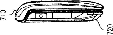
Figure 28 A to 28G is that application is according to the external view of the portable phone of the display device of above-mentioned any embodiment and so on.The coupling (hinge portion) 730 that this portable phone comprises upper shell 710 for example, lower house 720, couple upper shell 710 and lower house 720 mutually, display 740, slave display 750, picture lamp 760, and camera 770.Display 740 or slave display 750 are by disposing with the display device according to any above-described embodiment and so on.
(other variant)
With reference to the first and second embodiment, variant, and example application the present invention has been described.Yet, the invention is not restricted to these embodiment etc., but can carry out various modifications.
For example, can conceive, be write and the noisiness that causes can change according to the position on the display device (touch sensor) by aforesaid image among embodiment etc.Thereby, for the position of tackling noisiness relies on, preferably, in a plurality of zones each, prepare in embodiment etc. describes at operational formula mentioned above or look-up table.
And the example that has used as the side electric field patterns by the liquid crystal cell take the FFS pattern has been described the second embodiment.Yet, can use similarly the liquid crystal of IPS pattern.
And, in above-described embodiment etc., described the display device of liquid crystal cell as display element.Yet above-described embodiment etc. can be applied to use the display device such as other type display element of organic electroluminescent device.
In addition, in above-described embodiment etc., the situation that touch sensor is installed in display device has been described.Touch sensor is external type and the situation that is installed in display device exterior yet the present invention for example also can be applied to.
And any processing sequence in above-described embodiment etc. not only can be by hardware implement, and can be carried out by software.When the processing sequence was carried out by software, software program was installed on multi-purpose computer etc.Such program can be recorded in the recording medium that is built in computing machine in advance.
The application comprises with on May 18th, 2009 disclose relevant theme in the Japanese priority patent application JP 2009-120222 that Japan Office is submitted to, and its full content is contained in this by reference.
It will be appreciated by those skilled in the art that in the scope of claims and equivalents thereof, according to designing requirement and other factors, can carry out various modifications, combination, sub-portfolio, reach and replace.
Claims (15)
1. display device comprises:
A plurality of display pixel electrodes;
Public electrode is towards the display pixel electrode;
The Presentation Function layer has image display function;
Display control circuit comes carries out image to show control by applying pixel voltage to each display pixel electrode and applying common driver voltage to public electrode, and described common driver voltage and image show that the drive cycle of control is synchronously anti-phase;
Touch detecting electrode, cooperate to form capacitor with public electrode; And
Touch detection circuit, based on the detection signal that obtains from touching detecting electrode in response to the common driver voltage that is applied to public electrode, near the detection operation of the object execution detection is outside,
Wherein, based on the second detection signal that obtains at the first detection signal that obtains before the anti-phase timing with after anti-phase timing the two, described touch detection circuit is carried out described detection and is operated in the anti-phase period the anti-phase timing of common driver voltage after.
2. according to display device claimed in claim 1, wherein
Described touch detection circuit is by eliminating the detection signal that anti-phase rear noise obtains to eliminate noise from the second detection signal, described anti-phase rear noise is used for the picture signal write operation that image shows before by anti-phase timing to be caused, and affects the second detection signal; Then
The detection signal of noise is eliminated in described touch detection circuit utilization, carries out in the anti-phase period after anti-phase timing and detects operation.
3. according to display device claimed in claim 2, wherein
Described touch detection circuit is determined anti-phase front noise, and described anti-phase front noise is caused by the picture signal write operation that is used for the image demonstration before anti-phase timing, and affects the first detection signal; Then
Described touch detection circuit obtains to eliminate the detection signal of noise based on determined anti-phase front noise.
4. according to display device claimed in claim 3, wherein
Described touch detection circuit is based on the anti-phase rear noise of anti-phase front Noise sourse determination; And
Described touch detection circuit obtains to eliminate the detection signal of noise by deduct determined anti-phase rear noise from the second detection signal.
5. according to display device claimed in claim 3, wherein
The detection signal that described touch detection circuit obtains to eliminate noise by the predetermined operation formula pre-configured with reference to anti-phase front noise is used as parameter or look-up table.
6. according to display device claimed in claim 2, wherein
The detection signal that described touch detection circuit obtains to eliminate noise by the predetermined operation formula pre-configured with reference to the first and second detection signals are used as parameter or look-up table.
7. according to display device claimed in claim 1, wherein
The timing that described touch detection circuit was close to before anti-phase timing obtains the first detection signal.
8. according to display device claimed in claim 1, wherein
Described touch detection circuit the time before the picture signal write operation that is used for the image demonstration, was carried out and is detected operation in the anti-phase period after anti-phase timing.
9. according to display device claimed in claim 1, also comprise:
The circuit substrate that display control circuit is wherein arranged; And
Towards the relative substrate of circuit substrate,
Wherein, described display pixel arrangement of electrodes on the side near relatively substrate on the circuit substrate,
Described public electrode is arranged in the relative substrate near on the side of circuit substrate, and
Described Presentation Function layer is arranged as between the display pixel electrode and relatively suprabasil public electrode that is inserted on the circuit substrate.
10. according to display device claimed in claim 9, wherein
Described Presentation Function layer is liquid crystal layer.
11. according to display device claimed in claim 1, also comprise:
The circuit substrate that display control circuit is wherein arranged; And
Towards the relative substrate of circuit substrate,
Wherein, described public electrode and described display pixel electrode are stacking in order on circuit substrate, therebetween with insulation course, and
Described Presentation Function layer be arranged as the display pixel electrode that is inserted in circuit substrate and relatively in the substrate between.
12. according to the described display device of claim 11, wherein
Described Presentation Function layer is the liquid crystal layer that operates under the side electric field patterns.
13. according to display device claimed in claim 1, wherein
Described touch detecting electrode is divided into a plurality of strip electrode patterns.
14. according to the described display device of claim 13, wherein
Described display control circuit drives a plurality of electrode patterns in the mode that the group of the electrode pattern selected from a plurality of electrode patterns drives simultaneously, and the selection of group is shifted in order.
15. one kind comprises the electronic unit with the display device of touch sensor, described display device comprises:
A plurality of display pixel electrodes;
Public electrode is towards the display pixel electrode;
The Presentation Function layer has image display function;
Display control circuit comes carries out image to show control by applying pixel voltage to each display pixel electrode and applying common driver voltage to public electrode, and described common driver voltage and image show that the drive cycle of control is synchronously anti-phase;
Touch detecting electrode, cooperate to form capacitor with public electrode; And
Touch detection circuit, based on the detection signal that obtains from touching detecting electrode in response to the common driver voltage that is applied to public electrode, near the detection operation of the object execution detection is outside,
Wherein, based on the second detection signal that obtains at the first detection signal that obtains before the anti-phase timing with after anti-phase timing the two, described touch detection circuit is carried out detection and is operated in the anti-phase period the anti-phase timing of common driver voltage after.
Applications Claiming Priority (2)
| Application Number | Priority Date | Filing Date | Title |
|---|---|---|---|
| JP2009120222A JP5203291B2 (en) | 2009-05-18 | 2009-05-18 | Display device and electronic device |
| JP120222/09 | 2009-05-18 |
Publications (2)
| Publication Number | Publication Date |
|---|---|
| CN101893955A CN101893955A (en) | 2010-11-24 |
| CN101893955B true CN101893955B (en) | 2013-01-09 |
Family
ID=43068116
Family Applications (1)
| Application Number | Title | Priority Date | Filing Date |
|---|---|---|---|
| CN2010101779861A Expired - Fee Related CN101893955B (en) | 2009-05-18 | 2010-05-11 | Display device and electronic unit |
Country Status (5)
| Country | Link |
|---|---|
| US (1) | US9140922B2 (en) |
| JP (1) | JP5203291B2 (en) |
| KR (1) | KR101708057B1 (en) |
| CN (1) | CN101893955B (en) |
| TW (1) | TWI446251B (en) |
Families Citing this family (65)
| Publication number | Priority date | Publication date | Assignee | Title |
|---|---|---|---|---|
| US8643624B2 (en) * | 2009-03-18 | 2014-02-04 | Synaptics Incorporated | Capacitive sensing using a segmented common voltage electrode of a display |
| TWI395126B (en) * | 2009-07-20 | 2013-05-01 | Mstar Semiconductor Inc | Sensing apparatus and method applied to touch screen |
| US9922622B2 (en) * | 2010-02-26 | 2018-03-20 | Synaptics Incorporated | Shifting carrier frequency to avoid interference |
| EP2558927B1 (en) * | 2010-04-16 | 2022-06-15 | Microchip Technology Germany GmbH | Tft lc display and method for detecting the spatial position of limbs in a spatial region disposed in front of a display |
| US9898121B2 (en) | 2010-04-30 | 2018-02-20 | Synaptics Incorporated | Integrated capacitive sensing and displaying |
| EP2584437A2 (en) * | 2010-06-16 | 2013-04-24 | Samwon St | Touch panel sensor |
| JP2012014509A (en) * | 2010-07-01 | 2012-01-19 | On Semiconductor Trading Ltd | Capacitance type touch sensor |
| JP5458443B2 (en) | 2010-09-14 | 2014-04-02 | 株式会社ジャパンディスプレイ | Display device with touch detection function and electronic device |
| JP5307110B2 (en) * | 2010-12-01 | 2013-10-02 | 株式会社ジャパンディスプレイ | Touch panel |
| CN102096505A (en) * | 2011-01-07 | 2011-06-15 | 牧东光电(苏州)有限公司 | Touch panel jointed fragmentally and manufacturing method thereof |
| JP5927532B2 (en) * | 2011-03-22 | 2016-06-01 | 株式会社Joled | Display device and electronic device |
| JP5778961B2 (en) * | 2011-03-29 | 2015-09-16 | 株式会社Joled | Display device and electronic device |
| DE102011017383A1 (en) * | 2011-04-18 | 2012-10-18 | Ident Technology Ag | OLED interface |
| US20130038565A1 (en) * | 2011-08-10 | 2013-02-14 | Qualcomm Mems Technologies, Inc. | Touch sensing integrated with display data updates |
| US9470941B2 (en) * | 2011-08-19 | 2016-10-18 | Apple Inc. | In-cell or on-cell touch sensor with color filter on array |
| CN106249949B (en) | 2011-09-07 | 2018-03-20 | 辛纳普蒂克斯公司 | Capacitive sensing during non-display renewal time |
| KR101461036B1 (en) * | 2011-11-15 | 2014-11-14 | 엘지디스플레이 주식회사 | Apparatus and method for driving touch sensor |
| JP6022164B2 (en) * | 2012-01-24 | 2016-11-09 | 株式会社ジャパンディスプレイ | Liquid crystal display |
| US8970547B2 (en) | 2012-02-01 | 2015-03-03 | Synaptics Incorporated | Noise-adapting touch sensing window |
| KR20130096050A (en) * | 2012-02-21 | 2013-08-29 | 삼성디스플레이 주식회사 | Display device |
| WO2013140130A1 (en) * | 2012-03-21 | 2013-09-26 | Elliptic Laboratories As | Signal processing for acoustic user input |
| JP6071223B2 (en) * | 2012-03-26 | 2017-02-01 | 東芝ライフスタイル株式会社 | Electric vacuum cleaner |
| CN103368552A (en) * | 2012-04-11 | 2013-10-23 | 鸿富锦精密工业(深圳)有限公司 | Electronic equipment with touch keys |
| TWI469007B (en) * | 2012-04-17 | 2015-01-11 | Raydium Semiconductor Corp | Method of controlling noise processing circuit of touch panel and related signal processing device |
| TWI464642B (en) * | 2012-04-27 | 2014-12-11 | Orise Technology Co Ltd | In-cell multi-touch display panel system |
| JP5991709B2 (en) | 2012-05-01 | 2016-09-14 | 株式会社ジャパンディスプレイ | LCD with built-in touch panel |
| JP2013242432A (en) * | 2012-05-21 | 2013-12-05 | Panasonic Liquid Crystal Display Co Ltd | Liquid crystal display device |
| JP2013246289A (en) * | 2012-05-25 | 2013-12-09 | Panasonic Liquid Crystal Display Co Ltd | Liquid crystal display device |
| JP5979988B2 (en) * | 2012-05-31 | 2016-08-31 | 株式会社ジャパンディスプレイ | Liquid crystal display |
| JP6055206B2 (en) * | 2012-06-08 | 2016-12-27 | 株式会社ジャパンディスプレイ | Liquid crystal display |
| US10073568B2 (en) | 2012-08-15 | 2018-09-11 | Synaptics Incorporated | System and method for interference avoidance for a display device comprising an integrated sensing device |
| TWI469125B (en) * | 2012-08-31 | 2015-01-11 | Au Optronics Corp | Touch display apparatus and display-driving method |
| US10073550B2 (en) | 2012-09-20 | 2018-09-11 | Synaptics Incorporated | Concurrent input sensing and display updating |
| JP6037327B2 (en) * | 2012-09-24 | 2016-12-07 | 株式会社ジャパンディスプレイ | Liquid crystal display |
| KR101614057B1 (en) * | 2012-12-07 | 2016-04-20 | 엘지디스플레이 주식회사 | Display Device and Method for touch sensing of the same |
| TWI480781B (en) * | 2012-12-27 | 2015-04-11 | Ye Xin Technology Consulting Co Ltd | Touch screen device |
| CN103914166A (en) * | 2013-01-08 | 2014-07-09 | 东莞万士达液晶显示器有限公司 | Touch panel and driving method thereof |
| JP5865286B2 (en) * | 2013-03-29 | 2016-02-17 | 株式会社ジャパンディスプレイ | Electronic device and control method of electronic device |
| JP5865287B2 (en) * | 2013-03-29 | 2016-02-17 | 株式会社ジャパンディスプレイ | Electronic device and control method of electronic device |
| CN103218097B (en) * | 2013-04-07 | 2016-07-06 | 北京京东方光电科技有限公司 | A kind of capacitance type in-cell touch panel and display device |
| US9442615B2 (en) | 2013-10-02 | 2016-09-13 | Synaptics Incorporated | Frequency shifting for simultaneous active matrix display update and in-cell capacitive touch |
| KR102113622B1 (en) * | 2013-12-24 | 2020-05-21 | 엘지디스플레이 주식회사 | Display device and method for fabricating the same |
| US9372584B2 (en) * | 2014-01-09 | 2016-06-21 | Synaptics Incorporated | Mitigating electrode interference in an integrated input device |
| JP6375223B2 (en) * | 2014-01-31 | 2018-08-15 | 株式会社ジャパンディスプレイ | Display device with sensor and driving method thereof |
| TWI610203B (en) * | 2014-02-14 | 2018-01-01 | 晨星半導體股份有限公司 | Electrode of self-capacitive touch panel utilizing serpentine trace to increase resistance and self-capacitive touch panel |
| US9582099B2 (en) | 2014-03-31 | 2017-02-28 | Synaptics Incorporated | Serrated input sensing intervals |
| US9958720B2 (en) * | 2014-04-17 | 2018-05-01 | Japan Display Inc. | Display device |
| JP6442154B2 (en) * | 2014-04-23 | 2018-12-19 | 浜松ホトニクス株式会社 | Image acquisition apparatus and image acquisition method |
| US9298309B2 (en) | 2014-04-29 | 2016-03-29 | Synaptics Incorporated | Source driver touch transmitter in parallel with display drive |
| KR102249203B1 (en) * | 2014-09-05 | 2021-05-10 | 삼성전자주식회사 | Coordinate indicating apparatus and method for driving thereof |
| US10175827B2 (en) | 2014-12-23 | 2019-01-08 | Synaptics Incorporated | Detecting an active pen using a capacitive sensing device |
| JP6706621B2 (en) | 2015-01-05 | 2020-06-10 | シナプティクス インコーポレイテッド | Time division of display and sensing data |
| US10394391B2 (en) | 2015-01-05 | 2019-08-27 | Synaptics Incorporated | System and method for reducing display artifacts |
| TW202340820A (en) * | 2015-03-27 | 2023-10-16 | 日商半導體能源研究所股份有限公司 | Touch panel |
| JP6395651B2 (en) * | 2015-03-30 | 2018-09-26 | 株式会社ジャパンディスプレイ | Input device and display device |
| KR102355516B1 (en) * | 2015-04-30 | 2022-01-26 | 삼성디스플레이 주식회사 | Touch screen display device and driving method thereof |
| JP2016212561A (en) * | 2015-05-01 | 2016-12-15 | 株式会社ジャパンディスプレイ | Input device and display device |
| US10037112B2 (en) | 2015-09-30 | 2018-07-31 | Synaptics Incorporated | Sensing an active device'S transmission using timing interleaved with display updates |
| JP6134775B2 (en) * | 2015-12-22 | 2017-05-24 | 株式会社ジャパンディスプレイ | Electronic device and control method of electronic device |
| US10592022B2 (en) | 2015-12-29 | 2020-03-17 | Synaptics Incorporated | Display device with an integrated sensing device having multiple gate driver circuits |
| CN105426030A (en) * | 2016-01-05 | 2016-03-23 | 京东方科技集团股份有限公司 | Touch panel and display device |
| JP6535618B2 (en) * | 2016-02-16 | 2019-06-26 | 株式会社ジャパンディスプレイ | Display device |
| CN105589243A (en) * | 2016-03-23 | 2016-05-18 | 京东方科技集团股份有限公司 | Touch control display panel and display device |
| KR102365490B1 (en) | 2016-07-13 | 2022-02-18 | 가부시키가이샤 한도오따이 에네루기 켄큐쇼 | Input/output panel, input/output device, and semiconductor device |
| US11353754B2 (en) * | 2017-02-21 | 2022-06-07 | Semiconductor Energy Laboratory Co., Ltd. | Display panel, display device, input/output device, and data processing device |
Citations (3)
| Publication number | Priority date | Publication date | Assignee | Title |
|---|---|---|---|---|
| CN101131618A (en) * | 2006-08-20 | 2008-02-27 | 陈其良 | Pixel-multiplexing touch control type flat panel display |
| CN101305338A (en) * | 2006-03-08 | 2008-11-12 | 夏普株式会社 | Display device |
| CN101430436A (en) * | 2007-11-05 | 2009-05-13 | 爱普生映像元器件有限公司 | Display device and electronic apparatus |
Family Cites Families (10)
| Publication number | Priority date | Publication date | Assignee | Title |
|---|---|---|---|---|
| US6057903A (en) | 1998-08-18 | 2000-05-02 | International Business Machines Corporation | Liquid crystal display device employing a guard plane between a layer for measuring touch position and common electrode layer |
| JP2004021327A (en) * | 2002-06-12 | 2004-01-22 | Sharp Corp | Display device with touch sensor and positional data forming method |
| KR20050109223A (en) * | 2004-05-14 | 2005-11-17 | 삼성전자주식회사 | Apparatus and method for generating reference data for image signal modification |
| EP1821175A1 (en) * | 2004-10-22 | 2007-08-22 | Sharp Kabushiki Kaisha | Display device with touch sensor, and drive method for the device |
| JP2006146895A (en) * | 2004-10-22 | 2006-06-08 | Sharp Corp | Display device with touch sensor, and drive method for the same |
| US8259078B2 (en) * | 2006-06-09 | 2012-09-04 | Apple Inc. | Touch screen liquid crystal display |
| JP4733184B2 (en) * | 2006-06-12 | 2011-07-27 | シャープ株式会社 | Touch panel, display device, and method for manufacturing touch panel |
| JP2008009750A (en) | 2006-06-29 | 2008-01-17 | Casio Comput Co Ltd | Liquid crystal display element with touch panel |
| JP4453710B2 (en) * | 2007-03-19 | 2010-04-21 | セイコーエプソン株式会社 | Liquid crystal device, electronic apparatus and position detection method |
| JP2009093397A (en) * | 2007-10-09 | 2009-04-30 | Panasonic Corp | Touch panel and input device using the same |
-
2009
- 2009-05-18 JP JP2009120222A patent/JP5203291B2/en not_active Expired - Fee Related
-
2010
- 2010-04-19 TW TW099112219A patent/TWI446251B/en not_active IP Right Cessation
- 2010-04-30 US US12/771,759 patent/US9140922B2/en active Active
- 2010-05-10 KR KR1020100043347A patent/KR101708057B1/en active IP Right Grant
- 2010-05-11 CN CN2010101779861A patent/CN101893955B/en not_active Expired - Fee Related
Patent Citations (3)
| Publication number | Priority date | Publication date | Assignee | Title |
|---|---|---|---|---|
| CN101305338A (en) * | 2006-03-08 | 2008-11-12 | 夏普株式会社 | Display device |
| CN101131618A (en) * | 2006-08-20 | 2008-02-27 | 陈其良 | Pixel-multiplexing touch control type flat panel display |
| CN101430436A (en) * | 2007-11-05 | 2009-05-13 | 爱普生映像元器件有限公司 | Display device and electronic apparatus |
Also Published As
| Publication number | Publication date |
|---|---|
| KR101708057B1 (en) | 2017-02-17 |
| TW201044245A (en) | 2010-12-16 |
| KR20100124208A (en) | 2010-11-26 |
| JP2010267222A (en) | 2010-11-25 |
| CN101893955A (en) | 2010-11-24 |
| TWI446251B (en) | 2014-07-21 |
| US9140922B2 (en) | 2015-09-22 |
| US20100289765A1 (en) | 2010-11-18 |
| JP5203291B2 (en) | 2013-06-05 |
Similar Documents
| Publication | Publication Date | Title |
|---|---|---|
| CN101893955B (en) | Display device and electronic unit | |
| US9874976B2 (en) | Touch sensor, display device, and electronic apparatus | |
| US11009733B2 (en) | Detection device and display device | |
| CN101893957B (en) | Display device and electronic unit | |
| CN102112951B (en) | Touch sensor, display and electronic device | |
| US8633905B2 (en) | Touch sensor, display and electronic unit | |
| CN102375637B (en) | Display device and method, drive circuit and electronic equipment | |
| US8334851B2 (en) | Touch sensor, display and electronic unit | |
| JP5178633B2 (en) | Touch sensor, display device, and electronic device | |
| CN102236464A (en) | Display apparatus with touch detection functions, driving method, and electronic device | |
| JP2009205379A (en) | Display device with touch panel | |
| JP5497352B2 (en) | Display device and electronic device | |
| JP5893709B2 (en) | Display device and electronic device | |
| JP2013164871A (en) | Display device, and electronic apparatus | |
| KR20160082875A (en) | Touch sensor intergrated type display device |
Legal Events
| Date | Code | Title | Description |
|---|---|---|---|
| C06 | Publication | ||
| PB01 | Publication | ||
| C10 | Entry into substantive examination | ||
| SE01 | Entry into force of request for substantive examination | ||
| ASS | Succession or assignment of patent right |
Owner name: NIPPON DISPLAY CO., LTD. Free format text: FORMER OWNER: SONY CORPORATION Effective date: 20121105 |
|
| C41 | Transfer of patent application or patent right or utility model | ||
| TA01 | Transfer of patent application right |
Effective date of registration: 20121105 Address after: Aichi Applicant after: Japan display West Co.,Ltd. Address before: Tokyo, Japan Applicant before: Sony Corp. |
|
| C14 | Grant of patent or utility model | ||
| GR01 | Patent grant | ||
| CF01 | Termination of patent right due to non-payment of annual fee |
Granted publication date: 20130109 Termination date: 20210511 |
|
| CF01 | Termination of patent right due to non-payment of annual fee |